
LTC1574_1中文资料
4V < VIN < 16V, IPGM = 0V 4V < VIN < 16V SHDN = 0V, 4V < VIN < 16V
VLBTRIP ILBIN ILBOUT VHYST IPEAK RON tOFF VIH VIL
VLBOUT = 0.4V, VLBIN = 0V VLBOUT = 5V, VLBIN = 10V IPGM = VIN, VOUT = 0V IPGM = 0V, VOUT = 0V VOUT at Regulated Value Minimum Voltage at Pin 7 for Device to Be Active Maximum Voltage at Pin 7 for Device to Be in Shutdown
(Voltage Referred to GND Pin) Input Supply Voltage (Pin 5) ................. – 0.3V to 18.5V Switch Current (Pin 3, 14) ........................................ 1A Switch Voltage (Pin 3, 14) .......................... VIN – 18.5V Operating Temperature Range .................... 0°C to 70°C Junction Temperature (Note 2) ............................ 125°C Storage Temperature Range ................. – 65°C to 150°C Lead Temperature (Soldering, 10 sec).................. 300°C
SYMBOL PARAMETER IIH IIL VF IR SHDN Pin Input Current SHDN Pin Input Current Schottky Diode Forward Voltage Schottky Reverse Current CONDITIONS SHDN = 16V
1574 TA02
U
1
元器件交易网
LTC1574 LTC1574-3.3/LTC1574-5
ABSOLUTE
(Note 1)
AXI U
RATI GS
U U W PACKAGE/ORDER I FOR ATIO
TOP VIEW NC 1 GND 2 SW 3 GND 4 VIN 5 IPGM 6 SHDN 7 NC 8 16 NC 15 GND 14 SW 13 GND 12 LBIN 11 LBOUT 10 VOUT (VFB*) 9 NC
MIN TYP MAX 1
q q q
VIN = 6V to 12V, ILOAD = 100mA, IPGM = VIN (Note 3) LTC1574-3.3 (Note 3) LTC1574-5 (Note 3) 20mA < ILOAD < 175mA, IPGM = 0V 20mA < ILOAD < 400mA, IPGM = VIN 20mA < ILOAD < 175mA, IPGM = 0V 20mA < ILOAD < 400mA, IPGM = VIN
UNITS µA V V V mV mV mV mV mV µA µA µA V µA mA µA mV A A Ω µs V
1.20 3.14 4.75
1.25 3.30 5.00 10 –5 – 45 –5 – 50 450 130 2 1.25
1.30 3.46 5.25 70 – 70 – 70 – 70 – 70 600 180 25 1.4 0.5
0.5 7.5 0.54 0.27
1.0 15 0.60 0.34 0.9
1.5 1.0 30 0.83 0.53 1.55 5
3 1.2
4
0.75
V
元器件交易网
LTC1574 LTC1574-3.3/LTC1574-5
ELECTRICAL CHARACTERISTICS
ELECTRICAL CHARACTERISTICS
SYMBOL PARAMETER IFB VFB VOUT ∆VOUT Feedback Current into Pin 10 Feedback Voltage Regulated Output Voltage Output Voltage Line Regulation Output Voltage Load Regulation CONDITIONS LTC1574 LTC1574 LTC1574-3.3 LTC1574-5
q q q
2
U
W W
W
ORDER PART NUMBER LTC1574CS LTC1574CS-3.3 LTC1574CS-5
S PACKAGE 16-LEAD PLASTIC SO *ADJUSTABLE OUTPUT VERSION TJMAX = 125°C, θJA = 110°C/W
Consult factory for Industrial and Military grade parts.
U APPLICATIO S
s s s s s s
Inverting Converters Step-Down Converters Memory Backup Supply Portable Instruments Battery-Powered Equipment Distributed Power Systems
IQ
Input DC Supply Current (Note 4) Active Mode Sleep Mode Shutdown (Note 5) Low-Battery Trip Point Current into Pin 12 Current Sunk by Pin 11 Comparator Hysteresis Current Limit ON Resistance of Switch Switch Off Time SHDN Pin High SHDN Pin Low
The LTC®1574 is a family of easy-to-use current mode DC/DC converters ideally suited for 9V to 5V, 5V to 3.3V and inverting operation. With an internal 0.9Ω switch (at a supply voltage of 12V) and a low forward drop Schottky diode (0.450V typ at 200mA, TA = 25°C), the LTC1574 requires only three external components to construct a complete high efficiency DC/DC converter. Under no load condition, the LTC1574 draws only 130µA. In shutdown, it draws a mere 2µA making this converter ideal for battery-powered applications. In dropout, the internal P-channel MOSFET switch is turned on continuously allowing the user to maximize the life of the battery source. The maximum inductor current of the LTC1574 family is pin selectable to either 340mA or 600mA, optimizing efficiency for a wide range of applications. Operation up to 200kHz permits the use of small surface mount inductors and capacitors. For applications requiring higher output current or ultrahigh efficiency, see the LTC1148 or LTC1265 data sheets. For detailed applications information, see the LTC1174 data sheet.
LTC1574-5 Efficiency
100 95 L = 100µH VOUT = 5V IPGM = 0V VIN = 6V
5 VIN LBIN LTC1574-5 LBOUT IPGM GND 2, 4, 13, 15 VOUT SW SHDN 7 10 3, 14 100µH†
+
EFFICIENCY (%)
22µF* 35V
90 VIN = 9V 85 80 75 70
+
5V 175mA 100µF* 10V
1574 TA01
* AVX TPSD226K035 ** AVX TPSD107K010 † COILTRONICS CTX100-4
1
U
10 LOAD CURRENT (mA) 100 200
The q denotes specifications which apply over the full operating temperature range, otherwise specifications are at TA = 25°C. VIN = 9V, SHDN = VIN, IPGM = 0V, unless otherwise specified.
LTC4006资料

UNITS V mA % % % % % % % µA µA V V µA mA
–0.8 –1.0 –4 –5 –60 –35 –15 15 –10 4.2 1 4.7 1.6 – 10 2
VBAT < 6V, VCSP – VBAT Target = 10mV 6V ≤ VBAT ≤ VLOBAT, VCSP – VBAT Target = 10mV TTOL Shutdown Battery Leakage Current UVLO Undervoltage Lockout Threshold Shutdown Threshold at SHDN SHDN Pin Current Operating Current in Shutdown Current Sense Amplifier, CA1 Input Bias Current Into BAT Pin CMSL CMSH CA1/I1 Input Common Mode Low CA1/I1 Input Common Mode High
ELECTRICAL CHARACTERISTICS
SYMBOL IQ VTOL ITOL PARAMETER DCIN Operating Range Operating Current Charge Voltage Accuracy Charge Current Accuracy (Note 3)
CONDITIONS Sum of Current from CLP, CLN , DCIN Nominal Values: 12.3V, 12.6V, 16.4V, 16.8V (Note 2) q VCSP – VBAT Target = 100mV
q
MIN 6
TYP 3
TLC1549中文资料

TLC1549中文资料2009-08-14 21:52TLC1549C , TLC1549I , TLC1549M 10位模拟数字转换器(A/D)串行控制#10位分辨率A / D转换器#固有的采样保持#未经调整的总误差........± 1 LSB的最大值#片上系统时钟#终端兼容TLC549和TLV1549#CMOS工艺描述该TLC1549C , TLC1549I ,并TLC1549M 有10位,开关电容,successiveapproximation 模拟数字转换器。
这些器件有两个数字输入和一个3态输出[片选( CS )的,输入输出时钟( I / O时钟)和数据输出(数据) ]的提供三线接口,串口主机处理器。
该采样保持功能是自动的。
那个转换纳入这些设备的特点差分高阻抗基准投入便利比率转换,缩放,和隔离模拟电路的逻辑和供应噪音。
开关电容设计,让lowerror 转换的整个经营自由空气温度范围。
该TLC1549C运作的特点是从0 ° C至70 °角该TLC1549I的特点是操作从-40 ° C 至85 ° C该TLC1549M特点是操作,在整个军事温度范围 -55 ℃至125 ℃之间。
管脚说明:ANALOG IN (2):模拟信号输入。
驱动源阻抗应该是3月1日千瓦。
外部驱动源的模拟,应该有一个电流能力。
一十毫安。
CS (5):芯片选择。
高向低过渡的政务司司长重置内部计数器和控制,使数据和I / O时钟内最大的一个设置时间加上两个属于边缘内部系统时钟。
低到高过渡禁用I / O时钟设置时间内下降的边缘加两国的内部系统时钟。
DATA OUT (6):这3态串行输出的A / D转换结果是在高阻抗状态时,政务司司长高,积极当政务司司长低。
以有效的芯片选择,数据是从高阻抗状态,并驱车前往相应的逻辑电平的最高有效位价值先前的转换结果。
下一个下降沿的I / O 时钟驱动器DATAOUT的逻辑水平相应的下一个最重要的一点,其余位转移,以便与LSB的出现在第九届下降沿的I / O时钟。
LTC产品介绍
凌特是一个以提供高性能、高质量的模拟器件以及方案的提供商。
其公司产品共分为五大部分,分别为运算放大器、电源管理、数据转换器、接口类、以及RF/无线产品,其中每个大类中又根据产品的性能细分为各种产品。
运算放大器分类1、精密放大器,又分为零偏移和轨对轨两种细分,温漂小于0.1uV/℃,轨对轨产品的V os《1mV,这些技术参数相对于其他产品是其最大的优势所在,且输入电压的范围较宽,可用于精密仪器以及弱小信号的检测2、仪表放大器,有很高的增益精准度,开环增益可以做到很大,启动时间短,ns级别,温漂小,噪声小,用于机密仪器以及弱小信号的检测3、高速运算放大器,体现在其压摆很率SW很大,且增益带宽积也做到很大,可以保证信号的高速运算,而且信号噪声低,保证信号传输的稳定4、低功耗运算放大器。
功耗较低,正常工作时每个运放的工作电流只有几个mA甚至更小,噪声很低,用于便携设备5、差分运算放大器以及ADC驱动放大器。
可以不失真的传输高频信号,具有很高的压摆率,因此从功能上来说,与高速运算放大器也有一些共同点,可用于视频放大器以及AD转换器等产品6、从一些功能上划分还有低噪、低偏置电流,高温等各种用途的运算放大器,这些产品都是用在专业领域,也应该说凌特的产品都是用在比较专业的领域中,一些技术指标都是比较前沿的,不如TI,ADI等公司产品相对用途较为普遍。
)电源管理分类可分为LDO和DC-DC两大类,具有较高的基准电压(不知道你想表达什么意思)?,其中LDO产品输入电压范围大,噪声小,输出加很小的陶瓷电容就可以输出很稳定,压差可以做到很小,提高效率(去掉,LDO不是为了提高效率)。
DC-DC类产品又可分分为buck,boost,buck-boost类,电荷泵转换器、微型模块化电源芯片(可以并联使用,自动均衡,提高输出的功率,部分模块通过了EN55022 CLASS B的EMI测试报告,单位体积的功率密度做得比较大)等。
LTC1778-1资料
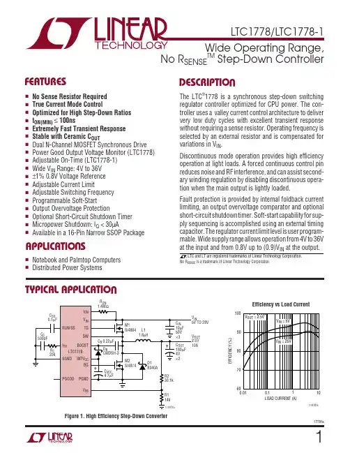
GN PART MARKING 17781
GN PACKAGE 16-LEAD PLASTIC SSOP TJMAX = 125°C, θJA = 130°C/ W
900 15 ITH = 1.2V (Note 3) VIN = 4V to 30V, ITH = 1.2V (Note 3) ITH = 0.5V to 1.9V (Note 3) VFB = 0.8V ITH = 1.2V (Note 3) VFCB = 0.8V ION = 30µA, VON = 0V (LTC1778-1) ION = 15µA, VON = 0V (LTC1778-1) ION = 180µA 198 396
The q denotes specifications which apply over the full operating temperature range, otherwise specifications are TA = 25°C. VIN = 15V unless otherwise noted.
q q q q
2000 30 0.808 – 0.3 ± 50 2 0.84 –2 268 536 100
µA µA V %/V % nA mS V µA ns ns ns
1778fa
0.792
0.800 0.002 – 0.05 –5
1.4 0.76
1.7 0.8 –1 233 466 50
元器件交易网
TYPICAL APPLICATIO
RON 1.4MΩ CSS 0.1µF RUN/SS CC 500pF ITH RC 20k SGND LTC1778 INTVCC BG ION VIN TG SW BOOST
M1 Si4884 CB 0.22µF DB CMDSH-3 M2 Si4874 CVCC 4.7µF
《LTCC元器件基础》课件

它是一种高性能、高可靠性的电 子元器件,广泛应用于航空航天 、军事、通信、汽车电子等领域 。
LTCC特点
01
02
03
04
高频性能优异
LTCC材料具有较低的介电常 数和介质损耗,适用于高频电
路。
集成度高
可以实现多层电路集成,减小 了元器件体积,提高了电路密
度。
可靠性高
LTCC材料具有较高的热导率 和机械强度,能够承受恶劣环
振荡器
总结词
高频率稳定性、低相位噪声、小型化
详细描述
LTCC振荡器利用低温共烧陶瓷的优良电气性能和多层布线技术,具有高频率稳定性和低相位噪声。此 外,LTCC振荡器可以实现小型化,广泛应用于各种通信系统和频率计量等领域。
04
LTCC元器件应用案例
手机中的LTCC元器件应用
总结词:小型电常数、低损耗、高稳定性
详细描述
LTCC电容器利用低温共烧陶瓷的优良介电性能,具有高介电常数和低损耗的特点 。这使得LTCC电容器具有高稳定性,能够满足各种高频、高稳定性的应用需求。
滤波器
总结词
高频率选择性、低插入损耗、小型化
详细描述
LTCC滤波器采用多层布线技术和低温 共烧陶瓷的高Q值特性,具有高频率 选择性和低插入损耗。此外,LTCC滤 波器可以实现小型化,方便集成到无 线通信等系统中。
航天器中的LTCC元器件应用
总结词:高精度、高稳定性、轻量化
航天器中使用的LTCC元器件需要具备高精度和高稳定性的特性,以确保航天器的安全和可靠性。LTCC技术在航天器中应用广 泛,如微波组件、天线、滤波器等。
05
LTCC元器件发展趋势与挑战
LTCC元器件发展趋势
01
LTC4151-1中文资料

ADR0 4
ADIN 5
TOP VIEW
10 SENSE– 9 GND 8 SDAO 7 SDAI 6 SCL
MS PACKAGE 10-LEAD PLASTIC MSOP
TJMAX = 125°C, θJA = 85°C/W
41511fa
2
元器件交易网
TOP VIEW
10 SENSE–
9 GND
11
8 SHDN
7 SDA
6 SCL
LTC4151-1
DD PACKAGE 10-LEAD (3mm s 3mm) PLASTIC DFN
TJMAX = 125°C, θJA = 45°C/W EXPOSED PAD (PIN 11) PCB GND CONNECTION OPTIONAL
0°C to 70°C
LTC4151IDD#PBF
LTC4151IDD#TRPBF
LCWZ
10-Lead (3mm x 3mm) Plastic DFN
–40°C to 85°C
LTC4151CDD-1#PBF
LTC4151CDD-1#TRPBF LCXC
10-Lead (3mm x 3mm) Plastic DFN
VIN = 48V, Normal Operation Mode VIN = 12V, Shutdown Mode VIN, SENSE+, SENSE– = 48V VIN, SENSE+, SENSE– = 48V
SHDN = 0V
l
7
80
V
l
1.2
1.7
mA
l
120
300
μA
LTC1484CN8资料
U APPLICATIO S
s Battery-Powered RS485/RS422 Applications s Low Power RS485/RS422 Transceiver s Level Translator
DESCRIPTIO
The LTC®1484 is a low power RS485 compatible transceiver. In receiver mode, it offers a fail-safe feature which guarantees a high receiver output state when the inputs are left open, shorted together or terminated with no signal present. No external components are required to ensure the high receiver output state.
s Guaranteed High Receiver Output State for Floating, Shorted or Terminated Inputs with No Signal Present
s Drives Low Cost Residential Telephone Wires s Low Power: ICC = 700µA Max with Driver Disabled s ICC = 900µA Max for Driver Enable with No Load s 20µA Max Quiescent Current in Shutdown Mode s Single 5V Supply s – 7V to 12mits ±7V
LTC1144资料
2
U
W
U
U
W W
W
元器件交易网
LTC1144 TYPICAL PERFORMANCE CHARACTERISTICS
Output Resistance vs Supply Voltage
元器件交易网
LTC1144 Switched-Capacitor Wide Input Range Voltage Converter with Shutdown
FEATURES
s s s s s s
DESCRIPTIO
s s
Wide Operating Supply Voltage Range: 2V to 18V Boost Pin (Pin 1) for Higher Switching Frequency Simple Conversion of 15V to –15V Supply Low Output Resistance: 120Ω Maximum Power Shutdown to 8µA with SHDN Pin Open Circuit Voltage Conversion Efficiency: 99.9% Typical Power Conversion Efficiency: 93% Typical Easy to Use
ORDER PART NUMBER LTC1144CN8 LTC1144IN8
N8 PACKAGE 8-LEAD PLASTIC DIP T JMAX = 110°C, θJA = 100°C/W
TOP VIEW BOOST 1 CAP+ 2 GND 3 CAP– 4 8 7 6 5 V+ OSC SHDN VOUT
LTC1144CS8 LTC1144IS8 S8 PART MARKING 1144 1144I
LTC4001资料
■Handheld Battery-Powered Devices ■Handheld Computers■Charging Docks and Cradles ■Digital Cameras ■Smart Phones2A Single Cell Li-Ion Battery ChargerBuck Li-Ion Charger■Low Power Dissipation■2A Maximum Charge Current■No External MOSFETs, Sense Resistor or Blocking Diode Required■Remote Sensing at Battery Terminals ■Programmable Charge Termination Timer■Preset 4.2V Float Voltage with ±0.5% Accuracy■Programmable Charge Current Detection/Termination ■Automatic Recharge■Thermistor Input for Temperature Qualified Charging ■Compatible with Current Limited Wall Adapters ■Low Profile 16-Lead (4mm × 4mm) QFN PackagePower Loss vs VBAT Charging (PWM Mode)FEATURESDESCRIPTIOUAPPLICATIO SUTYPICAL APPLICATIOUThe LTC ®4001 is a 2A Li-Ion battery charger intended for 5V wall adapters. It utilizes a 1.5MHz synchronous buck converter topology to reduce power dissipation during charging. Low power dissipation, an internal MOSFET and sense resistor allow a physically small charger that can be embedded in a wide range of handheld applications. The LTC4001 includes complete charge termination circuitry,automatic recharge and a ±1% 4.2V float voltage. Input short-circuit protection is included so no blocking diode is required.Battery charge current, charge timeout and end-of-charge indication parameters are set with external components.Additional features include shorted cell detection, tempera-ture qualified charging and overvoltage protection. The LTC4001 is available in a low profile (0.75mm) 16-lead (4mm × 4mm) QFN package.4.2V Li-IonV V BAT (V)3T O T A L A P P LI C A T I O N C I R C U I T P O W E R D I S S I P A T I O N (W )0.751.001.2544001 TA01b0.500.253.253.53.754.25Consult LTC Marketing for parts specified with wider operating temperature ranges.ABSOLUTE AXI U RATI GSW W WU PACKAGE/ORDER I FOR ATIOU U W(Note 1)LTC4001EUFORDER PART NUMBERUF PART MARKING4001T JMAX = 125°C, θJA = 37°C/WEXPOSED PAD (PIN 17) IS GND, MUST BE SOLDERED TO PCB161514135678TOP VIEW17UF PACKAGE16-LEAD (4mm × 4mm) PLASTIC QFN91011124321BAT SENSE PGND GNDSENS PROG NTC FAULT V INSENSEB A T S E N ST I M E RS SI D E TS WE NC H R GP V I NSYMBOL PARAMETER CONDITIONS MIN TYP MAX UNITSV IN Supply Voltage(Note 2)45.5V I INPV IN Connected to V INSENSE , PROG and IDET 2mA Pins Open, Charger On Shutdown, EN = V IN50µA V FLOAT V BAT Regulated Float Voltage Measured from BATSENS to GNDSENS ●4.158 4.2 4.242V 4.179 4.2 4.221V I BATCurrent Mode Charge CurrentR PROG = 549Ω, V BAT = 3.5V 1.82 2.2A R PROG = 1.10k, V BAT = 3.5V 0.91 1.1A Shutdown, EN = V IN ±5µA I TRIKL Trickle Charge Current V BAT = 2V 355065mA V TRIKL Trickle Charge Threshold V BAT Rising 3.05 3.1 3.20V V BAT Falling2.853.0 3.05V V UVL V IN Undervoltage Lockout Voltage V IN Rising, Measured from V INSENSE to GNDSENS 2.72.82V ∆V UVL V IN Undervoltage Lockout Hysteresis Measured from V INSENSE to GNDSENS100mV V ASD Automatic Shutdown Threshold V INSENSE – V BATSENS Rising (Turn-On), V BATSENSE = 4V 200250300mV VoltageV INSENSE – V BATSENS Falling (Turn-Off), V BATSENSE = 4V153060mV f OSC Oscillator Frequency 1.31.5 1.7MHz D Maximum Duty Factor 100%R PFET R DS(ON) of P-Channel MOSFET Measured from PV IN to SW 127m ΩR NFETR DS(ON) of N-Channel MOSFETMeasured from SW to PGND121m ΩThe ● denotes specifications which apply over the full operating temperature range, otherwise specifications are T A = 25°C.V IN = 5V, V EN = 0V, R PROG = 549Ω, R IDET = 549Ω, unless otherwise specified.ELECTRICAL CHARACTERISTICSOrder Options Tape and Reel: Add #TRLead Free: Add #PBF Lead Free Tape and Reel: Add #TRPBF Lead Free Part Marking: /leadfree/PV IN , V INSENSEt < 1ms, DC < 1%....................................–0.3V to 7V Steady State ............................................–0.3V to 6V SW, SENSE, BAT, BATSENS, SS, FAULT, CHRG, EN,NTC, PROG, IDET, TIMER Voltage.............. –0.3V to 6V Operating Temperature Range (Note 3)..–40°C to 85°C Operating Junction Temperature(Note 5)............................................... –40°C to 125°C Storage Temperature Range................ –65°C to 125°CSYMBOL PARAMETER CONDITIONS MINTYP MAXUNITSt TIMER Timer AccuracyC TIMER = 0.22µF ±10%V EN Enable Input Threshold Voltage V EN Rising0.60.81V ∆V EN Enable Input Hysteresis 100mV V PROG PROG Pin Voltage R PROG = 549Ω 1.213V V IDET IDET Pin Voltage R IDET = 549Ω 1.213V I IDET IDET ThresholdR IDET = 549Ω150200250mA I CHRG CHRG Pin Weak Pull-Down Current V CHRG = 1V 153050µA V CHRG CHRG Pin Output Low Voltage I CHRG = 5mA 0.20.4V V OL FAULT Pin Output Low Voltage 1mA Load 0.4V V OH FAULT Pin Output High Voltage 1mA Load4.6V V RECHRG Recharge Battery Threshold Voltage V FLOAT – V RECHRG V BAT Falling50100135mV t RB Recharge Filter Time Constant 4ms t RECHRG Recharge TimePercent of Total Charge Time50%t TRIKL Low-Battery Trickle Charge Time Percent of Total Charge Time, V BAT < 2.8V,25%Measured Using BATSENS and GNDSENS Pins I SS Soft-Start Ramp Current V BAT < V FLOAT – 100mV, V BAT Across BATSENS 612.816µAand GNDSENS Pins V COLDNTC Pin Cold Temperature Fault From NTC to GNDSENS Pin ThresholdRising Threshold 0.74 V INSENSE V Falling Threshold 0.72 V INSENSE V V HOTNTC Pin Hot Temperature Fault From NTC to GNDSENS Pin ThresholdFalling Threshold 0.29 V INSENSE V Rising Threshold 0.30 V INSENSEV V DIS NTC Disable Threshold (Falling)From NTC to GNDSENS Pin 0.015 •0.02 •0.025 •V V INSENSE V INSENSE V INSENSE∆V DISNTC Disable HysteresisFrom NTC to GNDSENS Pin0.01 • V INSENSEVThe ● denotes specifications which apply over the full operating temperature range, otherwise specifications are T A = 25°C.V IN = 5V, V EN = 0V, R PROG = 549Ω, R IDET = 549Ω, unless otherwise specified.ELECTRICAL CHARACTERISTICSNote 1: Stresses beyond those listed under Absolute Maximum Ratings may cause permanent damage to the device. Exposure to any Absolute Maximum Rating condition for extended periods may affect device reliability and lifetime.Note 2: Operation with current limited wall adapters is allowed down to the undervoltage lockout threshold.Note 3: The LTC4001E is guaranteed to meet performance specifications from 0°C to 85°C. Specifications over the –40°C to 85°C operatingtemperature range are assured by design, characterization and correlation with statistical process controls.Note 4: T J is calculated from the ambient temperature T A and power dissipation P D according to the following formula:T J = T A + (P D • 37°C/W)Note 5: This IC includes overtemperature protection that is intended to protect the device during momentary overload. Junction temperature will exceed 125°C when overtemperature protection is active. Continuous operation above the specified maximum operating junction temperature my impair device reliability.TYPICAL PERFOR A CE CHARACTERISTICS U WOscillator Frequency vs V INOscillator Frequency vs TemperatureDissipation of Figure 8 Circuit vs I BATPROG Pin Characteristic (V PROG vs I PROG )Dissipation of Figure 8 Circuit vs V INTrickle Charge Current vs V BATV FLOAT and Recharge BatteryThreshold Voltage vs TemperatureOutput Charging Characteristic Showing Constant Current and Constant Voltage Operation(T A = 25°C unless otherwise noted)V IN (V)3P E R C E N T V A R I A T I O N (%)–0.2500.25 4.55.54001 G01–0.50–0.75–1.003.5450.500.751.006I PROG (mA)00.81.0154001 G050.60.4510200.201.2V P R O G (V )V BAT (V)00I B A T (A )0.51.01.52.00.51 1.524001 G062.53 3.54V BAT (V)040I B A T (m A )4550550.511.524001 G072.53TEMPERATURE (°C)–50F R E Q U E N C Y V A R I A T I O N F R O M 25°C(%)0.40.60.81104001 G020.20–0.2–30–101030507090130150I BAT (mA)500T O T A L A P P L I C A T I O N C I R C U I T P O W E R D I S S I P A T I O N (W )0.500.754001 G030.2501000150020001.251.00V IN = 5V V BAT = 4VV IN (V)4.251.01.21.45.254001 G040.80.6 4.5 4.7555.50.40.20T O T A L A P P L I C A T I O N C I R C U I T P O W E R D I S S I P AT I O N (W )TEMPERATURE (°C)4.0F L O A T A N D R E C H A RG E V O L T A G E S(V )4.14.24.3–1030701104001 G08150–30–50105090130TYPICAL PERFOR A CE CHARACTERISTICSU WSoft-Start (PWM Mode)IDET Threshold vs R IDET for R PROG = 549ΩU U UPI FU CTIO SBAT (Pin 1): Battery Charger Output Terminal. Connect a 10µF ceramic chip capacitor between BAT and PGND to keep the ripple voltage small.SENSE (Pin 2): Internal Sense Resistor. Connect to exter-nal inductor.PGND (Pin 3): Power Ground.GNDSENS (Pin 4): Ground Sense. Connect this pin to the negative battery terminal. GNDSENS provides a Kelvin connection for PGND and must be connected to PGND schematically.SW (Pin 5): Switch Node Connection. This pin connects to the drains of the internal main and synchronous power MOSFET switches. Connect to external inductor.EN (Pin 6): Enable Input Pin. Pulling the EN pin high places the LTC4001 into a low power state where the BAT drain current drops to less than 3µA and the supply current is reduced to less than 50µA. For normal operation, pull the pin low.CHRG (Pin 7): Open-Drain Charge Status Output. When the battery is being charged, CHRG is pulled low by aninternal N-channel MOSFET. When the charge current drops below the IDET threshold (set by the R IDET program-ming resistor) for more than 5milliseconds, the N-channel MOSFET turns off and a 30µA current source is connected from CHRG to ground. (This signal is latched and is reset by initiating a new charge cycle.) When the timer runs out or the input supply is removed, the current source will be disconnected and the CHRG pin is forced to a high imped-ance state. A temperature fault causes this pin to blink.PV IN (Pin 8): Positive Supply Voltage Input. This pin connects to the power devices inside the chip. V IN ranges from 4V to 5.5V for normal operation. Operation down to the undervoltage lockout threshold is allowed with current limited wall adapters. Decouple with a 10µF or larger surface mounted ceramic capacitor.V INSENSE (Pin 9): Positive Supply Sense Input. This pin connects to the inputs of all input comparators (UVL, V IN to V BAT ). It also supplies power to the controller portion of this chip. When the BATSENS pin rises to within 30mV of V INSENSE , the LTC4001 enters sleep mode, dropping I IN to 50µA. Tie this pin directly to the terminal of the PV INdecoupling capacitor.CHRG Pin Temperature Fault Behavior (Detail)INPUTCURRENT (I IN )0.5A/DIVINDUCTOR CURRENT (I L )0.5A/DIVSOFT-START VOLTAGE (V SS )1V/DIV EN PIN (V )5V/DIV 0002ms/DIVV BAT = 3.5V V IN = 5V4001 G09R IDET (Ω)300I D E T (m A )20025030011004001 G101501005007009004001200600800100050400350CHRG 1V/DIVTIME (20µs/DIV)4001 G11FAULT (Pin 10): Battery Fault. This pin is a logic high if a shorted battery is detected or if a temperature fault is detected. A temperature fault occurs with the temperature monitor circuit enabled and the thermistor temperature is either below 0°C or above 50°C (typical).NTC (Pin 11): Input to the NTC (Negative Temperature Coefficient) Thermistor Temperature Monitoring Circuit.Under normal operation, tie a thermistor from the NTC pin to the GNDSENS pin and a resistor of equal value from NTC to V IN . When the voltage on this pin is above 0.74V IN (Cold,0°C) or below 0.29V IN (Hot, 50°C), charging is disabled and the CHRG pin blinks. When the voltage on NTC comes back between 0.74V IN and 0.29V IN , the timer continues where it left off and charging resumes. There is approxi-mately 3°C of temperature hysteresis associated with each of the input comparators. If the NTC function is not used connect the NTC pin to GNDSENS. This will disable all of the NTC functions. NTC should never be pulled above V IN .PRO G (Pin 12): Charge Current Program. The R PROG resistor connects from this pin to GNDSENS, setting the current:R k I PROG BAT AMPS =1110.()where I BAT is the high rate battery charging current.U U UPI FU CTIO SIDET (Pin 13): Charge Rate Detection Threshold. Connect-ing a resistor, R IDET to GNDSENS programs the charge rate detection threshold. If R IDET = R PROG , CHRG provides an I BAT /10 indication. For other thresholds see the Appli-cations Information section.SS (Pin 14): Soft-Start/Compensation. Provides soft-start function and compensation for the float voltage control loop and compensation for the charge current control loop. Tie a soft-start/compensation capacitor between this pin and GNDSENS.TIMER (Pin 15): Timer Capacitor. The timer period is set by placing a capacitor, C TIMER , to GNDSENS. Set C TIMER to:C TIMER = Time (Hrs) • 0.0733 (µF)where time is the desired charging time.Connect this pin to IDET to disable the timer. Connect this pin to GNDSENS to end battery charging when I BAT drops below the IDET charge rate threshold.BATSENS (Pin 16): Battery Sense Input. An internal resis-tor divider sets the final float voltage at this pin. The resistor divider is disconnected in sleep mode or when EN = H to reduce the battery drain current. Connect this pin to the positive battery terminal.Exposed Pad (Pin 17): Ground. This pin must be soldered to the PCB ground (PGND) for electrical contact and rated thermal performance.BLOCK DIAGRA WOPERATIOThe LTC4001 is a constant current, constant voltage Li-Ion battery charger based on a synchronous buck architecture. Low power dissipation makes continuous high rate (2A) battery charging practical. The battery DC charge current is programmed by a resistor R PROG (or a DAC output current) at the PROG pin. The final battery float voltage is internally set to 4.2V.Charging begins when the V IN voltage rises above the UVLO level (approximately 2.75V), V IN is 250mV greater than the battery voltage and EN is low. At the beginning of the charge cycle, if the battery voltage is less than the trickle charge threshold, 3V, the charger goes into trickle charge mode and delivers approximately 50mA to the battery using a linear charger. If the battery voltage stays low for more than one quarter of the charge time, the battery is considered faulty, the charge cycle is terminated and the FAULT pin produces a logic high output. When the battery voltage exceeds the trickle charge thresh-old, the low rate linear charger is turned off and the high rate PWM charger ramps up (based on the SS pin capaci-tance) reaching its full-scale constant current (set via the PROG pin). When the battery approaches the float voltage, the charge current will start to decrease. When the charge current drops below the charge rate detection threshold (set via the IDET pin) for more than 5ms, an internal comparator turns off the internal pull-down N-channel MOSFET at the CHRG pin, and connects a weak current source (30µA typical) to ground to indicate a near end-of-charge condition.Total charge time is set by an external capacitor connected to the timer pin. After timeout occurs, the charge cycle is terminated and the CHRG pin is forced to a high imped-ance state. To restart the charge cycle, remove and reapply the input voltage, or momentarily shut the charger down via the EN pin. Also, a new charge cycle will begin if the battery voltage drops below the recharge threshold volt-age (100mV below the float voltage). A recharge cycle lasts only one-half of the normal charge time.A negative temperature coefficient (NTC) thermistor lo-cated close to the battery pack can be used to monitor battery temperature and suspend charging when battery temperature is outside the 0°C to 50°C window. A tem-perature fault drives the FAULT pin high and makes the CHRG pin blink. When the input voltage (V IN) is present, the charger can be shut down by pulling the EN pin up. IDET BlankingThe IDET comparator provides an end-of-charge indica-tion by sensing when battery charge current is less than the IDET threshold. To prevent a false end-of-charge indication from occurring during soft-start, this compara-tor is blanked until the battery voltage approaches the float voltage.Automatic Battery RechargeAfter the charge cycle is completed and if both the battery and the input power supply (wall adapter) are still con-nected, a new charge cycle will begin if the battery voltage drops below 4.1V due to self-discharge or external load-ing. This will keep the battery near maximum capacity at all times without manually restarting the charge cycle.In some applications such as battery charging in GPRS cellphones, large load current transients may cause bat-tery voltage to momentarily drop below the recharge threshold. To prevent these transients from initiating a recharge cycle when it is not needed, the output of the recharge comparator is digitally qualified. Only if the battery voltage stays below the recharge threshold for at least 4ms will battery recharging occur. (GPRS qualifica-tion is available even if timeout is disabled.) Undervoltage Lockout and Automatic Shutdown Internal undervoltage lockout circuits monitor V IN and keep the charger circuits shut down until V IN rises above the undervoltage lockout threshold (3V). The UVLO has a built-in hysteresis of 100mV. Furthermore, to protect against reverse current, the charger also shuts down if V IN is less than V BAT. If automatic shutdown is tripped, V IN must increase to more than 250mV above V BAT to allow charging.OPERATIOOvervoltage, Chip Overtemperature and Short-Circuit Current ProtectionThe LTC4001 includes overvoltage, chip overtemperature and several varieties of short-circuit protection.A comparator turns off both chargers (high rate and trickle) if battery voltage exceeds the float voltage by approximately 5%. This may occur in situations where the battery is accidentally disconnected while battery charg-ing is underway.A comparator continuously monitors on-chip temperature and will shut off the battery charger when chip temperature exceeds approximately 160°C. Battery charging will be enabled again when temperature drops to approximately 150°C.Short-circuit protection is provided in several different ways. First, a hard short on the battery terminals will cause the charge to enter trickle charge mode, limiting charge current to the trickle charge current (typically 50mA). Second, PWM charging is prevented if the high rate charge current is programmed far above the 2A maximum recommended charge current (via the PROG pin). Third, an overcurrent comparator monitors the peak inductor current.APPLICATIO S I FOR ATIOW UUU Soft-Start and Compensation Capacitor Selection The LTC4001 has a low current trickle charger and a PWM-based high current charger. Soft-start is used when-ever the high rate charger is initially turned on, preventing high start-up current. Soft-start ramp rate is set by the internal 12.8µA pull-up current and an external capacitor.The control range on the SS pin is approximately 0.3V to 1.6V. With a 0.1µF capacitor, the time to ramp up to maximum duty cycle is approximately 10ms.The external capacitor on the SS pin also sets the compen-sation for the current control loop and the float voltage control loop. A minimum capacitance of 10nF is required.Charge Current and IDET ProgrammingThe LTC4001 has two different charge modes. If the battery is severely depleted (battery voltage less than 2.9V) a 50mA trickle current is initially used. If the battery voltage is greater than the trickle charge threshold, high rate charging is used.This higher charge current is programmable and is ap-proximately 915 times the current delivered by the PROG pin. This current is usually set with an external resistor from PROG to GNDSENS, but it may also be set with a current output DAC connected to the PROG pin. The voltage on the PROG pin is nominally 1.213V.For 2A charge current:R VAPROG =≅Ω915121325549•..The IDET threshold (a charge current threshold used to determine when the battery is nearly fully charged) is programmed in much the same way as the PROG pin,except that the IDET threshold is 91.5 times the current delivered by the IDET pin. This current is usually set with an external resistor from IDET to ground, but it may also be set with a current output DAC. The voltage on the PROG pin is nominally 1.213V.For 200mA IDET current (corresponding to C/10 for a 2AHr battery):R VAIDET =≅Ω9151213025549.•...1.10k Ω programs approximately 100mA and 274Ω ap-proximately 400mA.For applications where IDET is set to one tenth of the high rate charge current, and slightly poorer charger current and IDET threshold accuracy is acceptable, the PROG and IDET pins may be tied together and a single resistor, R1,can program both (Figure 1). R I CHARGE145751213=.•.andIDET I CHARGE =10Figure 1. Programming Charge Current and IDET Thresholdwith a Single Resistor114001fµF).APPLICATIO S I FOR ATIOW UUU124001fThe battery temperature is measured by placing a negative temperature coefficient (NTC) thermistor close to the battery pack. To use this feature, connect the NTC ther-mistor, R NTC , between the NTC pin and GNDSENS and the resistor, R NOM , from the NTC pin to V INSENSE . R NOM should be a 1% resistor with a value equal to the value of the chosen NTC thermistor at 25°C. The LTC4001 goes into hold mode when the resistance, R HOT , of the NTC thermistor drops to 0.41 times the value of R NOM . For instance for R NTC = 10k. (The value for a Vishay NTHS0603N02N1002J thermistor at 25°C) hold occurs at approximately 4.1k, which occurs at 50°C. The hold mode freezes the timer and stops the charge cycle until the thermistor indicates a return to a valid temperature. As the temperature drops, the resistance of the NTC thermistor rises. The LTC4001 is designed to go into hold mode when the value of the NTC thermistor increases to 2.82 times the value of R NOM . This resistance is R COLD . For the Vishay 10k thermistor, this value is 28.2k, which corresponds to approximately 0°C. The hot and cold comparators each have approximately 3°C of hysteresis to prevent oscilla-tion about the trip point. Grounding the NTC pin disables the NTC function.ThermistorsThe LTC4001 NTC trip points were designed to work with thermistors whose resistance temperature characteristics follow Vishay Dale’s “R-T Curve 2.” However, any ther-mistor whose ratio of R COLD to R HOT is about 7 will also work (Vishay Dale R-T Curve 2 shows a ratio of R COLD to R HOT of 2.815/0.4086 = 6.89).Power conscious designs may want to use thermistors whose room temperature value is greater than 10k. Vishay Dale has a number of values of thermistor from 10k to 100k that follow the “R-T Curve 1.” Using these as indi-cated in the NTC Thermistor section will give temperature trip points of approximately 3°C and 47°C, a delta of 44°C.This delta in temperature can be moved in either direction by changing the value of R NOM with respect to R NTC .Increasing R NOM will move the trip points to higher tem-peratures. To calculate R NOM for a shift to lower tempera-ture for example, use the following equation:R R R at C NOM COLDNTC =°281525.• where R COLD is the resistance ratio of R NTC at the desired cold temperature trip point. If you want to shift the trip points to higher temperatures use the following equation:R R R at CNOM HOTNTC =°0408625.• where R HOT is the resistance ratio of R NTC at the desired hot temperature trip point.Here is an example using a 100k R-T Curve 1 thermistor from Vishay Dale. The difference between trip points is 44°C, from before, and we want the cold trip point to be 0°C, which would put the hot trip point at 44°C. The R NOM needed is calculated as follows:R R R at C k k NOM COLDNTC =°==28152532662815100116.• ..•The nearest 1% value for R NOM is 115k. This is the value used to bias the NTC thermistor to get cold and hot trip points of approximately 0°C and 44°C respectively. To extend the delta between the cold and hot trip points a resistor, R1, can be added in series with R NTC (see Figure 4). The values of the resistors are calculated as follows:R R R R R R R NOM COLD HOT COLD HOT HOT==()–.–...–.•––281504086104086281504086APPLICATIO S I FOR ATIOW UUU134001fwhere R NOM is the value of the bias resistor, R HOT and R COLD are the values of R NTC at the desired temperature trip points. Continuing the example from before with a desired hot trip point of 50°C:R R R k k k is nearest R k k k is nearest NOM COLD HOT ==()==()⎛⎝⎜⎞⎠⎟=–.–.•.–..–..,%•..–.•.–.–..,.%281504086100326360360228150408612081211110004086281504086326603602036021331331The final solution is as shown if Figure 4 where R NOM =121k, R1 = 13.3k and R NTC = 100k at 25°C.Input and Output CapacitorsThe LTC4001 uses a synchronous buck regulator to pro-vide high battery charging current. A 10µF chip ceramicAPPLICATIO S I FOR ATIOW UUU capacitor is recommended for both the input and output capacitors because it provides low ESR and ESL and can handle the high RMS ripple currents. However, some high Q capacitors may produce high transients due to self-resonance under some start-up conditions, such as con-necting the charger input to a hot power source. For more information, refer to Application Note 88.EMI considerations usually make it desirable to minimize ripple current in the battery leads, and beads or inductors may be added to increase battery impedance at the 1.5MHz switching frequency. Switching ripple current splits be-tween the battery and the output capacitor depending on the ESR of the output capacitor and the battery impedance.If the ESR of the output capacitor is 0.1Ω and the battery impedance is raised to 2Ω with a bead or inductor, only 5%of the ripple current will flow in the battery. Similar techniques may also be applied to minimize EMI from the input leads.Figure 4. Extending the Delta Temperature4001 F04144001fInductor SelectionA high (1.5MHz) operating frequency was chosen for the buck switcher in order to minimize the size of the inductor.However, take care to use inductors with low core losses at this frequency. A good choice is the IHLP-2525AH-01from Vishay Dale.To calculate the inductor ripple current:∆=I V V V L fL BAT BAT IN –•2where V BAT is the battery voltage, V IN is the input voltage,L is the inductance and f is the PWM oscillator frequency (typically 1.5MHz). Maximum inductor ripple current oc-curs at maximum V IN and V BAT = V IN /2.Peak inductor current will be:I PK = I BAT + 0.5 • ∆I Lwhere I BAT is the maximum battery charging current.When sizing the inductor make sure that the peak current will not exceed the saturation current of the inductors.Also, ∆I L should never exceed 0.4(I BAT ) as this may interfere with proper operation of the output short-circuit protection comparator. 1.5µH provides reasonable induc-tor ripple current in a typical application. With 1.5µH and 2A charge current:∆=µ=I V V V H MHz A L P 2852855515150612.–...•..-Pand I PK = 2.31AAPPLICATIO S I FOR ATIOW UUU Remote SensingFor highest float voltage accuracy, tie GNDSENS and BATSENS directly to the battery terminals. In a similar fashion, tie BAT and PGND directly to the battery termi-nals. This eliminates IR drops in the GNDSENS and BATSENS lines by preventing charge current from flowing in them.Operation with a Current Limited Wall Adapter Wall adapters with or without current limiting may be used with the LTC4001, however, lowest power dissipation battery charging occurs with a current limited wall adapter.To use this feature, the wall adapter must limit at a current smaller than the high rate charge current programmed into the LTC4001. For example, if the LTC4001 is pro-grammed to charge at 2A, the wall adapter current limit must be less than 2A.To understand operation with a current limited wall adapter,assume battery voltage, V BAT , is initially below V TRIKL , the trickle charge threshold (Figure 5). Battery charging be-gins at approximately 50mA, well below the wall adapter current limit so the voltage into the LTC4001 (V IN ) is the wall adapter’s rated output voltage (V ADAPTER ). Battery voltage rises eventually reaching V TRIKL . The linear charger shuts off, the PWM (high rate) charger turns on and a soft-start cycle begins. Battery charging current rises during the soft-start cycle causing a corresponding increase in wall adapter load current. When the wall adapter reaches current limit, the wall adapter output voltage collapses and the LTC4001 PWM charger duty cycle ramps up to 100%(the topside PMOS switch in the LTC4001 buck regulator stays on continuously). As the battery voltage approaches V FLOAT , the float voltage error amplifier commands the PWM charger to deliver less than I LIMIT . The wall adapter exits current limit and the V IN jumps back up to V ADAPTER .。
HI-1574资料
1573CDI 1573CDT 1573CDM 1574CDI 1574CDT 1574CDM
18 TXINHA 17 RXA 16 RXA 15 TXB 14 TXB 13 TXINHB 12 RXB 11 RXB
元器件交易网
HI-1573, HI-1574
PIN DESCRIPTIONS
FUNCTION
power supply analog output analog output digital input power supply power supply analog output analog output digital input power supply digital output digital output digital input digital input digital input digital output digital output digital input digital input digital input
FEATURES
! Compliant to MIL-STD-1553A & B,
ARINC 708A
! 3.3V single supply operation ! Smallest footprint available in 20 pin plastic
ESOIC (thermally enhanced SOIC) package
DESCRIPTION
The HI-1573 and HI-1574 are low power CMOS dual transceivers designed to meet the requirements of the MIL-STD-1553 specification. The transmitter section of each channel takes complementary CMOS / TTL digital input data and converts it to bi-phase Manchester encoded 1553 signals suitable for driving the bus isolation transformer. Separate transmitter inhibit control signals are provided for each transmitter. The receiver section of the each channel converts the 1553 bus bi-phase data to complementary CMOS / TTL data suitable for inputting to a Manchester decoder. Each receiver has a separate enable input which can be used to force the output of the receiver to a logic "0" (HI-1573) or logic 1 (HI-1574). To minimize the package size for this function, the transmitter outputs are internally connected to the receiver inputs, so that only two pins are required for connection to each coupling transformer. For designs requiring independent access to transmitter and receiver 1553 signals, please contact your Holt Sales representative.