MAX5900LBETT-T中文资料
万高产品速选表
A(63-250A) 内置式 AC220V 50Hz/60Hz
b b b b v b b b
0, 5, 15, 30 0, 5, 15, 30 b -
备注:■ 为标准配置,□ 为选配 “*”为仅在选配电流监测模块后具有此功能。
B (63-630A) 装置式 AC220V 50Hz/60Hz
b b b b b b b b b v b b b
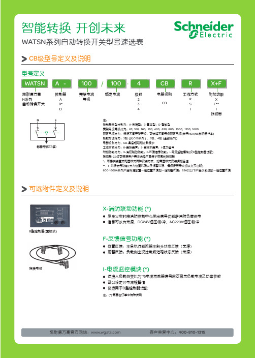
WATSN 100-630A PC级型号定义与说明
Ք(ࡽޙPCप)
WATSN 施耐德万高
N系列 自动转换开关
B-
160/ 160 ·
控制器 壳架电流 额定电流
A B* D
4 极数
3 4
PC
R
X
电器级别 工作方式 附加功能
PC
R
X
S
F
I
I
控制器类型:A-末端型;B-基本型;D-智能型 壳架电流等级:100, 160, 250, 400, 630 额定电流等级:100, 160, 250, 400, 630 极数:3-3极;4-4极 电器级别:PC级 工作方式:R-自投自复;S-自投不自复;I-互为备用 附加功能:X-消防联动;F-反馈信号功能;I-电流监测模块(仅D型控制器可选) *可提供装置式和面板式两种安装方式,如需面板式安装请在订货时备注说明
b v
通讯
电流监测模块
A型
b b b b b b b
b b
b 0-63秒 b 0-63秒 b b -
-
备注:■ 为标准配置,□ 为选配
B型
b b b b b b b b b b b
b b b
b 0-255秒 b 0-255秒 b b b -
Maxxt中文使用说明书

, .
:
:
.
.
,
.
.
. BW
.
,
.
180 6
2
GasAlert MAX XT II
GasAlertMax XT II
.
50% LEL .
.
,
,
BW
,
,
BW
. ,
,
.
:
LEL
.
,
,
.
20.9%(V/V)
GasAlertMax XT II
. ,
.
.
,
. .
BW
: : 1-800-663-4164
: 86-800-988-1586
1
GasAlert MAX XT II
GasAlertMax XT II
.
GasAlertMax XT II
. GasAlertMax XT II
.
.
.
GasAlertMax XT II
-
)
○30
.
Latched Alarms ,
, .
, LCD Latching Alarms
Fleet Manager II .
, .
10
GasAlert MAX XT II
GasAlertMax XT II :
Fleet Manager II
, Fleet Manager II . l.
:
:
(
on Self-Test
:
:
MAX809SN160T1资料
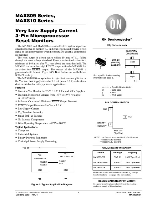
MAX809 Series,MAX810 SeriesVery Low Supply Current 3-Pin Microprocessor Reset MonitorsThe MAX809 and MAX810 are cost–effective system supervisor circuits designed to monitor V CC in digital systems and provide a reset signal to the host processor when necessary. No external components are required.The reset output is driven active within 10 µsec of V CC falling through the reset voltage threshold. Reset is maintained active for a minimum of 140 msec after V CC rises above the reset threshold. The MAX810 has an active–high RESET output while the MAX809 has an active–low RESET output. The output of the MAX809 is guaranteed valid down to V CC = 1.0 V. Both devices are available in a SOT–23 package.The MAX809/810 are optimized to reject fast transient glitches on the V CC line. Low supply current of 1.0 µA (V CC= 3.2 V) makes these devices suitable for battery powered applications.Features•Precision V CC Monitor for 2.5 V, 3.0 V, 3.3 V, and 5.0 V Supplies •Precision Monitoring V oltages from 1.6 V to 4.9 V Availablein 100 mV Steps•140 msec Guaranteed Minimum RESET Output Duration •RESET Output Guaranteed to V CC = 1.0 V•Low Supply Current•V CC Transient Immunity•Small SOT–23 Package•No External Components•Wide Operating Temperature: –40°C to 105°CTypical Applications•Computers•Embedded Systems•Battery Powered Equipment•Critical µP Power Supply MonitoringV CCFigure 1. Typical Application DiagramDevice Package ShippingORDERING INFORMATIONMAX809xTR SOT–233000 Tape/Reel MAX809SNxxxT1SOT–233000 Tape/Reel NOTE:*SOT–23 is equivalent to JEDEC (TO–236) **RESET is for MAX809***RESET is for MAX810SOT–23(TO–236)CASE 318PIN CONFIGURATION312V CCGNDRESET**SOT–23*(Top View)xx, xxx= Specific Device Codem= Date Codey= Yearw= Work WeekMARKINGDIAGRAMS32xxxm1(RESET)***MAX810xTR SOT–233000 Tape/ReelSee general marking information in the device marking section on page 8 of this data sheet.DEVICE MARKING INFORMATION NOTE: The “x” and “xxx” denotes a suffix for V cc voltage threshold options – see page 8 for more details.32xxyw1See specific device markinginformation on page 8.PIN DESCRIPTIONABSOLUTE MAXIMUM RATINGS* (Note 1)1.This device series contains ESD protection and exceeds the following tests:Human Body Model 2000 V per MIL–STD–883, Method 3015. Machine Model Method 350 V.2.The maximum package power dissipation limit must not be exceeded.P D +T J(max)*T Aq JAwith T J(max) = 150°C ELECTRICAL CHARACTERISTICS T A = –40°C to +105°C unless otherwise noted. Typical values are at T A = +25°C. (Note 3)The following data is given for MAX809 threshold levels: 1.60 V, 2.32 V, 2.93 V, 4.63 V and 4.90 V.AELECTRICAL CHARACTERISTICS(continued) T A = –40°C to +105°C unless otherwise noted. Typical values are at T A = +25°C. (Note 4) The following data is given for MAX809 threshold levels: 1.60 V, 2.32 V, 2.93 V, 4.63 V and 4.90 V.A5.Contact your ON Semiconductor sales representative for other threshold voltage options.ELECTRICAL CHARACTERISTICS (V CC = Full Range, T A = –40°C to +85°C unless otherwise noted. Typical values are at T A = +25°C, V CC = 5.0 V for L/M/J, 3.3 V for T/S, 3.0 V for R) (Note 6) The following data is given for MAX809 threshold levels: 2.63 V, 3.08 V, 4.00 V and 4.38 V; MAX810 threshold levels: 2.63 V, 2.93 V, 3.08 V, 4.38 V and 4.63 V.AAPPLICATIONS INFORMATIONV CC Transient RejectionThe MAX809 provides accurate V CC monitoring and reset timing during power–up, power–down, and brownout/sag conditions, and rejects negative–going transients (glitches)on the power supply line. Figure 2 shows the maximum transient duration vs. maximum negative excursion (overdrive) for glitch rejection. Any combination of duration and overdrive which lies under the curve will not generate a reset signal. Combinations above the curve are detected as a brownout or power–down. Typically, transient that goes 100 mV below the reset threshold and lasts 5 µs or less will not cause a reset pulse. Transient immunity can be improved by adding a capacitor in close proximity to the V CC pin of the MAX809.Figure 2. Maximum Transient Duration vs. Overdrivefor Glitch Rejection at 25°CV CC10.010080110.060.0M A X I M U M T R A N S I E N T D U R A T I O N (µs e c )20120RESET COMPARATOR OVERDRIVE (mV)160.06040RESET Signal Integrity During Power–DownThe MAX809 RESET output is valid to V CC = 1.0 V .Below this voltage the output becomes an “open circuit” and does not sink current. This means CMOS logic inputs to the µP will be floating at an undetermined voltage. Most digital systems are completely shutdown well above this voltage.However, in situations where RESET must be maintainedvalid to V CC = 0 V , a pull–down resistor must be connected from RESET to ground to discharge stray capacitances and hold the output low (Figure 3). This resistor value, though not critical, should be chosen such that it does not appreciably load RESET under normal operation (100 k W will be suitable for most applications).Figure 3. Ensuring RESET Valid to V CC = 0 VProcessors With Bidirectional I/O PinsSome µP’s (such as Motorola 68HC11) have bi–directional reset pins. Depending on the current drive capability of the processor pin, an indeterminate logic level may result if there is a logic conflict. This can be avoided by adding a 4.7 k W resistor in series with the output of the MAX809 (Figure 4). If there are other components in the system which require a reset signal, they should be buffered so as not to load the reset line. If the other components are required to follow the reset I/O of the µP, the buffer should be connected as shown with the solid line.Figure 4. Interfacing to Bidirectional Reset I/OBUFFERED RESETThe following data is given for MAX809 threshold levels: 1.60 V, 2.32 V, 2.93 V, 4.63 V and 4.90 V.1.10S U P P L Y C U R R E N T I N M I C R O A M PTEMPERATURE (°C)N O R M A L I Z E D P O W E R –U P R E S E T T I M E O U T–404020–206080Figure 7. Normalized Power–Up Reset vs.Temperature Figure 8. Normalized Reset Threshold Voltagevs. TemperatureTEMPERATURE (°C)–404020–206080The following data is given for MAX809 threshold levels: 2.63 V, 3.08 V, 4.00 V and 4.38 V;MAX810 threshold levels: 2.63 V, 2.93 V, 3.08 V, 4.38 V and 4.63 V.S U P P L Y C U R R E N T ( A )m 040206080100P O W E R -D O W N R E S E T D E L A Y ( s e c )m TEMPERATURE (C °)-40-200204085Figure 13. Power–Up Reset Timeout vs.Temperature TEMPERATURE (C °)-40-20020406085225235230240245250P O W E R -U P R E S E T T I M E O U T (m s e c )60Figure 14. Normalized Reset Threshold vs.TemperatureTAPING FORMComponent Taping Orientation for 3L SOT–23 (JEDEC–236) Devices(Mark Right Side Up)SOT–23Package Carrier Width (W)Pitch (P)Part Per Full ReelReel Size 8 mm4 mm30007 inchesTape & Reel Specifications TableMARKING AND THRESHOLD INFORMATIONm = Date Codey = Yearw = Work WeekPACKAGE DIMENSIONSSOT–23PLASTIC PACKAGE (TO–236)CASE 318–08ISSUE AHNOTES:1.DIMENSIONING AND TOLERANCING PER ANSI Y14.5M, 1982.2.CONTROLLING DIMENSION: INCH.3.MAXIMUM LEAD THICKNESS INCLUDES LEADNotesNotes11ON Semiconductor and are trademarks of Semiconductor Components Industries, LLC (SCILLC). SCILLC reserves the right to make changes without further notice to any products herein. SCILLC makes no warranty, representation or guarantee regarding the suitability of its products for any particular purpose, nor does SCILLC assume any liability arising out of the application or use of any product or circuit, and specifically disclaims any and all liability, including without limitation special, consequential or incidental damages. “Typical” parameters which may be provided in SCILLC data sheets and/or specifications can and do vary in different applications and actual performance may vary over time. All operating parameters, including “Typicals” must be validated for each customer application by customer’s technical experts. SCILLC does not convey any license under its patent rights nor the rights of others.SCILLC products are not designed, intended, or authorized for use as components in systems intended for surgical implant into the body, or other applications intended to support or sustain life, or for any other application in which the failure of the SCILLC product could create a situation where personal injury or death may occur. Should Buyer purchase or use SCILLC products for any such unintended or unauthorized application, Buyer shall indemnify and hold SCILLC and its officers, employees, subsidiaries, affiliates, and distributors harmless against all claims, costs, damages, and expenses, and reasonable attorney fees arising out of, directly or indirectly, any claim of personal injury or death associated with such unintended or unauthorized use, even if such claim alleges that SCILLC was negligent regarding the design or manufacture of the part. SCILLC is an Equal Opportunity/Affirmative Action Employer. PUBLICATION ORDERING INFORMATIONJAPAN: ON Semiconductor, Japan Customer Focus Center4–32–1 Nishi–Gotanda, Shinagawa–ku, Tokyo, Japan 141–0031Phone: 81–3–5740–2700Email: r14525@。
Boonton PMX40 RF Power Meter数据手册说明书

The PMX40 provides design engineers and technicians the utility of traditional benchtop instrument, the flexibility and performance of modern USB RF power sensors, and the simplicity of a multi-touch display built with Boonton award-winning technology.As a benchtop meter, the PMX40 provides a standalone solution for capturing, displaying, and analyzing peak and average RF power in both the time and statistical domains through an intuitive, multi-touch touchscreen display.The PMX40 Power Meter utilizes up to four RTP and CPS families of USB RF power sensors with industry- leading performance and capabilities either independently or for synchronized multi-channel measurements of CW, modulated, and pulsed signals.Providing the ultimate flexibility, the PMX40 sensors can be disconnected and independently used as standalone instruments.Key Features• Capture/display/analyze peak and average power• Frequency range from 4 kHz to 40 GHz• Industry-leading video bandwidth (195 MHz) and rise time (3 ns)• Industry-leading 100,000 measurements per second• Industry-leading 100 ps time resolution• Synchronous multi-channel measurements (up to 4 channels)• Sensors can be used as standalone instruments PMX40 RF Power MeterPulsed ModeAnalysis of fast-rising single pulses or pulses with short pulserepetition intervals (PRIs) requires an instrument with sophisticated trigger and data acquisition capability. Within Pulsed Mode, more than 16 pulse parameters can be measured.Continuous ModeFor simple, intuitive measurements of repetitive waveforms, the PMX40 Continuous Mode of operation provides a numeric display of average, maximum and minimum signal powers.Statistical ModeIn Statistical Mode, the PMX40 plots the Complementary Cumulative Distribution Function (CCDF). The CCDF plot shows the rate of occurrence of a specific crest factor for signals, such as those used in 5G, 4G/LTE, and Wi-Fi applications.PMX40 RF Power Meter – Front PanelConnect up to 4 USB sensors for multi-channel measurements.Multi-touch display with intuitive user interface.One touch to quickly access presets and favorite functions.Sync ports to source or receive triggers for timing and synchronization.Test source to verify sensor operation.The PMX40’s intuitive, multi-touch display enables fast configuration of up to four sensors as well as easy access to measurement and analysis tools, providing a standalone solution for capturing, displaying, and analyzing peak and average RF power in both the time and statistical domains. The meter also incorporates a test source to verify sensor operation.High-Performance and Versatile USB Power Sensors• Real-Time Power Processing™ technology with virtually zero measurement latency • 100,000 measurements per second • 80 dB dynamic range• Synchronized multi-channel measurementsAll RTP Real-Time Power SensorsThe Boonton PMX40 Power Meter utilizes Boonton RTP and CPS families of USB RF power sensors with indus-try leading performance and capabilities. All RTP sensors incorporate the unique Boonton Real-Time Power Processing™ technology, which virtually eliminates gaps in measurement suffered by other power sensors and enables industry best measurement speeds. In terms of RF performance, the RTP5000 series Real-Time Peak Power Sensors are the fastest responding sensors with 3 ns rise times and 195 MHz of video bandwidth. The RTP4000 series Real-Time True Average Power Sensors enable the lowest frequency measurements for diode-based average power measuring sensors and can make accurate measurements virtually independent of signal modulation bandwidth. CPS sensors offer flexible connectivity and performance leadership at anexcellent price point.Real-Time Power Processing™Boonton Real-Time Power Processing 1 dramatically reduces the total cycle time for acquiring and processing power measurement samples. By combining a dedicated acquisition engine, hardware trigger, integrated sample buffer, and a real-time optimized parallel processing architecture, Real-Time Power Processing™ performs most of the sweep processing steps simultaneously, beginning immediately after the trigger instead of waiting for the end of the acquisition cycle.The advantages of the Real-Time Power Processing technique are that key processing steps take place in parallel and keep pace with the signal acquisition. With no added computational overhead to prolong the sweep cycle, the sample buffer cannot overflow. As a result, there is no need to halt acquisition for trace processing. This means gap-free signal acquisition virtually guarantees that intermittent signal phenomena such as transients or dropouts will be reliably captured and analyzed.1RTPP is available within the RTP500 and RTP4000 sensors.Software FeaturesMeasurement Buffer ModeThe RTP series Measurement Buffer Mode is a remote control function that works in conjunction with Real-Time Power Processing to provide only therelevant burst or pulse information, eliminating the need to download and post-process large sample buffers. As a result, users can collect and analyze measurements from a virtually unlimited number of consecutive pulses or events without gaps. A wide variety of parameters can be calculated and plotted, such as duty cycle, pulse repetition rate, pulse width variation, and pulse jitter. In addition, anomalies,such as dropouts, can be identified.Dropouts, such as those shown left, are the sorts of events often missed by conventional power meters due to the acquisition gaps while processing takes place.Example seven pulse waveform.Measurement buffer data returned for waveform in above.Wi-Fi and Wireless Communication Signal AnalysisCharacterization and compliance testing of Wi-Fi and LTE chipsets and devices involves significant challenges for design and test engineers. With multiple-input, multiple-output (MIMO) architectures and channel bandwidths up to 160 MHz, testing is complex, especially when measuring RF power per channel and time alignment between channels. The PMX40 enables packet power measurements to be performed independently on multiple synchronous or asynchronous transmit chains with a common timebase shared among sensors.Use markers to define a portion of the waveform on which to make measurements. “Between Marker” measurements are ideal for monitoring specific portions of a packet over long intervals.Video bandwidth (VBW) describes the ability of a power sensor to track peak (envelope) power. Insufficient VBW will result in errant envelope and average power measurements. The PMX40 offers the widest video bandwidth (195 MHz) making it ideal for measuring 80 MHz, 100 MHz, and 160MHz channels.By comparing the peak-to-average power ratio, or crest factor (CF), of input and output signals of an RF transmission chain, engineers can assess circuit linearity. Additional insight can be provided with the PMX40 statistical mode Complementary Cumulative Distribution Function (CCDF) plot displaying the rate of occurrence of a specific CF. As an amplifier output compresses, the CF will reduce and the CCDF plot will move left.Indication of amplifier output compressionCrest FactorSecondary Surveillance Radar (SSR)Design, verification, troubleshooting and maintenance of secondary surveillanceradar (e.g. IFF-based radar) has never been more demanding.Proper design and operation of SSR systems is critical to the safety and security of aviation. The PMX40 can b e u sed t o easily a nd accurately capture SSR waveforms. Markers enable measurements on specific portions of the waveform.Industry-leading rise time (<3 ns) enables characterization of the most demanding radar signals.Utilize the superior 100 ps time resolution to zoom and uncover signal characteristics that might otherwise be missed.Key Features and Functionality• Data displayed as numerical meter or waveform trace • Statistical analysis with CCDF plot• Multiple marker measurements, including between marker data and marker ratios • Automated measurements; e.g., 16 automated pulse measurements • Export measurement data in .csv or .pdf formats • Up to 8 simultaneous power measurement channels• Simulation mode available to preview functionality when a sensor is not availableKey Features and Functionality• Large numeric readout and/or analog meter display • Zoom and pan through data logging strip chart• Quickly set frequency, aperture (averaging) and offset values all from the main screen• Calculates ratios between sensor measurements • Control up to 8 sensors at once• Simulation mode available to preview functionality when a sensor is not availableSensor SoftwarePower Viewer – Simple and Intuitive Measurement Software(for standalone operation of the CPS2000 Series of sensors)Power Viewer is a complimentary PC-based software package for CPS2008 sensor control, measurement configuration, and analysis. It includes USB drivers, remote control API, firmware updater and virtual instrument application.(for standalone operation of the RTP4000 and RTP5000 series of sensors)Power Analyzer is a complimentary PC-Based software package for RTP5000 and RTP4000 sensor control, measurement configuration, and advanced analysis. It includes USB drivers, remote control API, firmwareupdater and virtual instrument application.Power Analyzer - Advanced Measurement and Analysis SoftwareSensor SpecificationsRTP5006RTP5318 RF Frequency Range50 MHz to 6 GHz50 MHz to 18 GHz Dynamic RangeSpecificationsChannels Up to 4 Sensors RTP5000 SeriesRTP4000 SeriesCPS2000 Series Display5-inch WVGA multi-touch display with intuitive graphical user interfaceDisplay Modes Trace (power vs time)Statistical measurements Meter (numeric display)CCDFAutomatic measurements (pulse, statistical, and markers measurements)Marker Measurements (in Trace View)Markers (vertical cursors)Marker IndependentlyInterval Between MarkersPair of MarkersSettable in time relative to the trigger positionAvg, Min and Max Power at a specified time offsetAvg, Min and Max Power over the defined intervalRatio of power values at each markerPulse Mode – Automatic Measurements Pulse rise-timePulse widthPulse periodPulse duty cyclePulse peakPulse overshootTop level powerEdge delayPulse fall-timePulse off-timePulse repetition frequencyWaveform averagePulse averagePulse droopBottom level powerPulse edge skew between channelsStatistical Mode –Automatic Measurements Peak powerMinimum powerDynamic rangeCrest factor at cursorAverage powerPeak to average ratioPercent at cursorCrest factor at various percentsTrigger Synchronization*ModeSourceInternal Level RangeExternal Level RangeSlopeHold-off, Min Pulse Width, Max Trigger RateAmong RTP Series(internal trig distribution)Normal, Auto, Auto Pk-to-Pk, Free Run Any connected RTP Series sensor (via SMB’s) or rearpanel external trigger -40 dBm to +20 dBm (sensor dependent)±5 volts or TTL+ or -Sensor and timebase dependentTime Base Time Base Resolution, Range, AccuracyTime Base DisplayTrigger Delay RangeTrigger Delay ResolutionSensor dependent Sweeping or Roll Mode Sensor dependent0.02 divisionsSpecifications, ContinuedInputs/Outputs (front panel)USB with SMB trigger port Test Source50 MHz(optional rear panel placement)Inputs/Outputs (rear panel)LANUSB with SMB trigger portWireless Telecom Group Inc. 25 Eastmans Rd Parsippany, NJ United StatesTel: +1 973 386 9696 Fax: +1 973 386 9191 © Copyright 2020 All rights reserved.B/PMX40/0520/ENNote: Specifications, terms and conditions are subject to change without prior notice.PMX40RF Power Meter (includes 2 active channels)OptionsPMX40-4CH PMX40-GPIB PMX40-RTSAdds 2 Active Channels (for a total of 4)GPIB Control (internally installed)Moves Test Source output to the rear panelIncluded AccessoriesInformation Card (provides information on where to download the latest manual, software, utilities)Optional AccessoriesPMX40-RMK PMX40-TCASEFull-width 19” Rack Mount Kit (includes handles & hardware for mounting one or two meters)Transit case, hold the PMX40 and up to 4 sensorsRF Power SensorsCPS2008RTP4006RTP4106RTP4018*RTP4040*RTP5006RTP5318RTP5518RTP5340RTP5540True Average Connected Power Sensor Real-Time True Average Power Sensor Real-Time True Average Power Sensor Real-Time True Average Power Sensor Real-Time True Average Power Sensor Real-Time Peak Power Sensor Real-Time Peak Power Sensor Real-Time Peak Power Sensor Real-Time Peak Power Sensor Real-Time Peak Power Sensor50 MHz to 8 GHz 10 MHz to 6 GHz 4 kHz to 6 GHz 10 MHz to 18 GHz 10 MHz to 40 GHz 50 MHz to 6 GHz 50 MHz to 18 GHz 50 MHz to 18 GHz 50 MHz to 40 GHz 50 MHz to 40 GHzIncluded AccessoriesInformation Card (provides information on where to download the latest manual, software, utilities)0.9 m BNC (m) to SMB (m) cable (RTP sensors)0.9 m SMB (m) to SMB (m) cable (RTP sensors)1.8 m USB A (m) to USB B (m) locking SeaLATCH cable (RTP sensors)1.6 m USB A (m) to USB B (m) cable (CPS sensors)Ordering Information*RTP4018 and RTP4040 are currently in development. Specifications and performance subject to change。
INTERSIL X9C102 X9C103 X9C104 X9C503 说明书

®X9C102, X9C103, X9C104, X9C503Digitally Controlled Potentiometer (XDCP™)FEATURES•Solid-state potentiometer•3-wire serial interface•100 wiper tap points—Wiper position stored in nonvolatile memory and recalled on power-up•99 resistive elements—Temperature compensated—End to end resistance, ±20%—Terminal voltages, ±5V•Low power CMOS—V CC = 5V—Active current, 3mA max.—Standby current, 750µA max.•High reliability—Endurance, 100,000 data changes per bit —Register data retention, 100 years•X9C102 = 1kΩ•X9C103 = 10kΩ•X9C503 = 50kΩ•X9C104 = 100kΩ•Packages—8 Ld SOIC and 8 Ld PDIP•Pb-free plus anneal available (RoHS compliant)DESCRIPTIONThe X9Cxxx are Intersil digitally controlled (XDCP) potentiometers. The device consists of a resistor array, wiper switches, a control section, and nonvola-tile memory. The wiper position is controlled by a three-wire interface.The potentiometer is implemented by a resistor array composed of 99 resistive elements and a wiper switch-ing network. Between each element and at either end are tap points accessible to the wiper terminal. The position of the wiper element is controlled by the CS, U/D, and INC inputs. The position of the wiper can be stored in nonvolatile memory and then be recalled upon a subsequent power-up operation.The device can be used as a three-terminal potentiom-eter or as a two-terminal variable resistor in a wide variety of applications including:–control–parameter adjustments–signal processingBLOCK DIAGRAMDeviceSSGeneralDetailed L/V L W/V W H/V HH/R HW/VL/R L SelectPIN DESCRIPTIONS Pin Symbol Brief Description1INC Increment . The INC input is negative-edge triggered. Toggling INC will move the wiper and either increment or decrement the counter in the direction indicated by the logic level on the U/D input.2U/D Up/Down. The U/D input controls the direction of the wiper movement and whether the counter is incremented or decremented.3R H /V HR H /V H . The high (V H /R H ) terminals of the X9C102/103/104/503 are equivalent to the fixedterminals of a mechanical potentiometer. The minimum voltage is -5V and the maximum is +5V. The terminology of V H /R H and V L /R L references the relative position of the terminal inrelation to wiper movement direction selected by the U/D input and not the voltage potential on the terminal.4V SS V SS5V W /R W V W /R W . V W /R W is the wiper terminal, and is equivalent to the movable terminal of a mechanical potentiometer. The position of the wiper within the array is determined by the control inputs. The wiper terminal series resistance is typically 40Ω.6R L /V LR L /V L . The low (V L /R L ) terminals of the X9C102/103/104/503 are equivalent to the fixedterminals of a mechanical potentiometer. The minimum voltage is -5V and the maximum is +5V. The terminology of V H /R H and V L /R L references the relative position of the terminal inrelation to wiper movement direction selected by the U/D input and not the voltage potential on the terminal.7CSCS. The device is selected when the CS input is LOW. The current counter value is stored innonvolatile memory when CS is returned HIGH while the INC input is also HIGH. After the store op-eration is complete the X9C102/103/104/503 device will be placed in the low power standby mode until the device is selected once again.8V CCV CCABSOLUTE MAXIMUM RATINGSTemperature under bias....................-65°C to +135°C Storage temperature.........................-65°C to +150°C Voltage on CS, INC, U/D and V CCwith respect to V SS ..................................-1V to +7V Voltage on V H /R H and V L /R Lreferenced to V SS ...................................-8V to +8V ΔV = |V H /R H - V L /R L |X9C102 ...............................................................4V X9C103, X9C503, and X9C104.........................10V Lead temperature (soldering, 10 seconds)......+300°C I W (10 seconds).................................................8.8mA Power rating X9C102........................................16mW Power rating X9C103/104/503..........................10mWCOMMENT Stresses above those listed under “Absolute Maximum Ratings” may cause permanent damage to the device.This is a stress rating only; functional operation of the device (at these or any other conditions above those listed in the operational sections of this specification) is not implied. Exposure to absolute maximum rating conditions for extended periods may affect device reliability.POTENTIOMETER CHARACTERISTICS (Over recommended operating conditions unless otherwise stated.)Notes:(1)Absolute linearity is utilized to determine actual wiper voltage versus expected voltage = [V W(n)(actual) - V W(n)(expected )] = ±1 MI Maximum. (2)Relative linearity is a measure of the error in step size between taps = V W(n + 1) - [V W(n) + MI ] = +0.2 MI.(3) 1 MI = Minimum Increment = R TOT /99(4)Typical values are for T A = +25°C and nominal supply voltage.(5)This parameter is not 100% tested.Symbol ParameterLimitsUnit Test Conditions/NotesMin.Typ.Max.R TOTAL End to end resistance variation -20+20%V VH/RH V H terminal voltage -5+5V V VL/RL V L terminal voltage -5+5V I W Wiper current -4.44.4mA R WWiper resistance 40100ΩWiper Current = ±1mA Noise (5)-120dBV Ref. 1kHzResolution 1%Absolute linearity (1)-1+1MI (3)V W(n)(actual) - V W(n)(expected)Relative linearity (2)-0.2+0.2MI (3)V W(n + 1)(actual) - [V W(n)+MI ]RTOTAL temperature coefficient ±300(5)ppm/°C X9C103/503/104RTOTAL temperature coefficient ±600(5)ppm/°C X9C102Ratiometric temperature coefficient±20ppm/°C C H /C L /C W(5)Potentiometer capacitances10/10/25pFSee Circuit #3, Macro ModelRECOMMENDED OPERATING CONDITIONS Temperature mercial 0°C +70°C Industrial-40°C+85°CSupply Voltage (V CC )Limits X9C102/103/104/5035V ±10%ENDURANCE AND DATA RETENTIONA.C. CONDITIONS OF TEST Symbol ParameterLimitsUnit Test ConditionsMin.Typ.(4)Max.I CC V CC active current 13mA CS = V IL , U/D = V IL or V IH and INC=****************CYC I SB Standby supply current 200750µA CS = V CC - 0.3V, U/D and INC = V SS or V CC -0.3V I LI CS, INC, U/D input leakage current±10µA V IN = V SS to V CCV IH CS, INC, U/D input HIGH voltage2VV IL CS, INC, U/D input LOW voltage0.8V C IN (5)CS, INC, U/D input capacitance10pFV CC = 5V, V IN = V SS , T A = 25°C, f = 1MHzParameter Min.UnitMinimum endurance 100,000Data changes per bit per registerData retention100yearsInput pulse levels 0V to 3V Input rise and fall times 10ns Input reference levels1.5VTest Circuit #1Test Circuit #2Test Circuit #3Test Point V W /R W V R /R HV SV L /R LForce Current V H /R HTest PointV W /R WV L /R LR HC H10pFC W R LC LR WR TOTAL25pF10pFMacro ModelPOWER-UP AND DOWN REQUIREMENTSAt all times, voltages on the potentiometer pins must be less than ±V CC . The recall of the wiper position from nonvola-tile memory is not in effect until the V CC supply reaches its final value. The V CC ramp rate spec is always in effect.A.C. TIMINGNotes:(6)Typical values are for T A = 25°C and nominal supply voltage.(7) This parameter is periodically sampled and not 100% tested.(8)MI in the A.C. timing diagram refers to the minimum incremental change in the V W output due to a change in the wiper position.Symbol ParameterLimitsUnit Min.Typ.(6)Max.t Cl CS to INC setup100ns t lD INC HIGH to U/D change 100ns t DI U/D to INC setup 2.9µs t lL INC LOW period 1µs t lH INC HIGH period1µs t lC INC inactive to CS inactive 1µs t CPH CS deselect time (STORE)20ms t CPH CS deselect time (NO STORE)100ns t IW (5)INC to V W/RW change 100µs t CYC INC cycle time2µs t R , t F (5)INC input rise and fall time 500µs t PU (5)Power-up to wiper stable 500µs t R V CC (5)V CC power-up rate0.250V/msCSINCU/DV Wt CIt ILt IHt CYCt IDt DIt IWMI(8)t ICt CPHt Ft R10%90%90%DETAILED PIN DESCRIPTIONS R H /V H and R L /V LThe high (V H /R H ) and low (V L /R L ) terminals of the X9C102/103/104/503 are equivalent to the fixed termi-nals of a mechanical potentiometer. The minimum voltage is -5V and the maximum is +5V. The terminol-ogy of V H /R H and V L /R L references the relative position of the terminal in relation to wiper movement direction selected by the U/D input and not the voltage potential on the terminal.R W /V WV W /R W is the wiper terminal, and is equivalent to the movable terminal of a mechanical potentiometer. The position of the wiper within the array is determined by the control inputs. The wiper terminal series resistance is typically 40Ω.Up/Down (U/D)The U/D input controls the direction of the wiper move-ment and whether the counter is incremented or dec-remented.Increment (INC)The INC input is negative-edge triggered. Toggling INC will move the wiper and either increment or decre-ment the counter in the direction indicated by the logic level on the U/D input.Chip Select (CS)The device is selected when the CS input is LOW.The current counter value is stored in nonvolatile memory when CS is returned HIGH while the INC input is also HIGH. After the store operation is com-plete the X9C102/103/104/503 device will be placed in the low power standby mode until the device is selected once again.PIN CONFIGURATIONPIN NAMESPRINCIPLES OF OPERATIONThere are three sections of the X9Cxxx: the input con-trol, counter and decode section; the nonvolatile mem-ory; and the resistor array. The input control section operates just like an up/down counter. The output of this counter is decoded to turn on a single electronic switch connecting a point on the resistor array to the wiper output. Under the proper conditions the contents of the counter can be stored in nonvolatile memory and retained for future use. The resistor array is com-prised of 99 individual resistors connected in series. At either end of the array and between each resistor is an electronic switch that transfers the potential at that point to the wiper.The wiper, when at either fixed terminal, acts like its mechanical equivalent and does not move beyond the last position. That is, the counter does not wrap around when clocked to either extreme.The electronic switches on the device operate in a “make before break” mode when the wiper changes tap positions. If the wiper is moved several positions,multiple taps are connected to the wiper for t IW (INC to V W /R W change). The R TOTAL value for the device can temporarily be reduced by a significant amount if the wiper is moved several positions.When the device is powered-down, the last wiper posi-tion stored will be maintained in the nonvolatile mem-ory. When power is restored, the contents of the memory are recalled and the wiper is set to the value last stored.V CC CS V L /R L V W /R WINC U/D V SS12348765V H /R H X9C102/103/104/503DIP/SOICSymbol DescriptionV H /R H High Terminal V W /R W Wiper Terminal V L /R L Low Terminal V SS Ground V CC Supply Voltage U/D Up/Down Control Input INC Increment Control Input CS Chip Select Control Input NCNo ConnectionINSTRUCTIONS AND PROGRAMMINGThe INC, U/D and CS inputs control the movement of the wiper along the resistor array. With CS set LOW the device is selected and enabled to respond to the U/D and INC inputs. HIGH to LOW transitions on INC will increment or decrement (depending on the state of the U/D input) a seven-bit counter. The output of this counter is decoded to select one of one-hundred wiper positions along the resistive array.The value of the counter is stored in nonvolatile mem-ory whenever CS transitions HIGH while the INC input is also HIGH.The system may select the X9Cxxx, move the wiper, and deselect the device without having to store the lat-est wiper position in nonvolatile memory. After the wiper movement is performed as described above and once the new position is reached, the system must keep INC LOW while taking CS HIGH. The new wiper position will be maintained until changed by the sys-tem or until a power-down/up cycle recalled the previ-ously stored data.This procedure allows the system to always power-up to a preset value stored in nonvolatile memory; then during system operation minor adjustments could be made. The adjustments might be based on user pref-erence: system parameter changes due to tempera-ture drift, etc...The state of U/D may be changed while CS remains LOW. This allows the host system to enable the device and then move the wiper up and down until the proper trim is attained.MODE SELECTIONSYMBOL TABLECS INC U/D ModeL H Wiper UpL L Wiper DownH X Store Wiper PositionH X X Standby CurrentL X No Store, Return to StandbyL H Wiper Up (not recommended)L L Wiper Down (not recommended)WAVEFORM INPUTS OUTPUTSMust besteadyWill besteadyMay changefrom Lo w toHighWill changefrom Lo w toHighMay changefrom High toLowWill changefrom High toLowDon’t Care:ChangesAllowedChanging:State NotKnownN/A Center Lineis HighImpedancePERFORMANCE CHARACTERISTICSContact the factory for more information.APPLICATIONS INFORMATIONElectronic digitally controlled (XCDP) potentiometers provide three powerful application advantages; (1) the variability and reliability of a solid-state potentiometer, (2) the flexibility of computer-based digital controls, and (3) the retentivity of nonvolatile memory used for the storage of multiple potentiometer settings or data.Basic Configurations of Electronic PotentiometersV RBasic CircuitsX9C102, X9C103, X9C104, X9C503Small Outline Package Family (SO)GAUGE PLANEA2A1LL1DETAIL X4° ±4°SEATING PLANEeHbC0.010BM C A 0.004C0.010BM C A BD(N/2)1E1EN(N/2)+1APIN #1I.D. MARKh X 45°ASEE DETAIL “X”c0.010MDP0027SMALL OUTLINE PACKAGE FAMILY (SO)SYMBOLSO-8SO-14SO16 (0.150”)SO16 (0.300”) (SOL-16)SO20 (SOL-20)SO24 (SOL-24)SO28 (SOL-28)TOLERANCENOTESA 0.0680.0680.0680.1040.1040.1040.104MAX -A10.0060.0060.0060.0070.0070.0070.007±0.003-A20.0570.0570.0570.0920.0920.0920.092±0.002-b 0.0170.0170.0170.0170.0170.0170.017±0.003-c 0.0090.0090.0090.0110.0110.0110.011±0.001-D 0.1930.3410.3900.4060.5040.6060.704±0.0041, 3E 0.2360.2360.2360.4060.4060.4060.406±0.008-E10.1540.1540.1540.2950.2950.2950.295±0.0042, 3e 0.0500.0500.0500.0500.0500.0500.050Basic -L 0.0250.0250.0250.0300.0300.0300.030±0.009-L10.0410.0410.0410.0560.0560.0560.056Basic -h 0.0130.0130.0130.0200.0200.0200.020Reference -N 8141616202428Reference-Rev. L 2/01NOTES:1.Plastic or metal protrusions of 0.006” maximum per side are not included.2.Plastic interlead protrusions of 0.010” maximum per side are not included.3.Dimensions “D” and “E1” are measured at Datum Plane “H”.4.Dimensioning and tolerancing per ASME Y14.5M -199411All Intersil U.S. products are manufactured, assembled and tested utilizing ISO9000 quality systems.Intersil Corporation’s quality certifications can be viewed at /design/qualityIntersil products are sold by description only. Intersil Corporation reserves the right to make changes in circuit design, software and/or specifications at any time without notice. Accordingly, the reader is cautioned to verify that data sheets are current before placing orders. Information furnished by Intersil is believed to be accurate and reliable. However, no responsibility is assumed by Intersil or its subsidiaries for its use; nor for any infringements of patents or other rights of third parties which may result from its use. No license is granted by implication or otherwise under any patent or patent rights of Intersil or its subsidiaries.For information regarding Intersil Corporation and its products, see FN8222.1December 20, 2006X9C102, X9C103, X9C104, X9C503Plastic Dual-In-Line Packages (PDIP)MDP0031PLASTIC DUAL-IN-LINE PACKAGESYMBOLPDIP8PDIP14PDIP16PDIP18PDIP20TOLERANCENOTESA 0.2100.2100.2100.2100.210MAX A10.0150.0150.0150.0150.015MIN A20.1300.1300.1300.1300.130±0.005b 0.0180.0180.0180.0180.018±0.002b20.0600.0600.0600.0600.060+0.010/-0.015c 0.0100.0100.0100.0100.010+0.004/-0.002D 0.3750.7500.7500.890 1.020±0.0101E 0.3100.3100.3100.3100.310+0.015/-0.010E10.2500.2500.2500.2500.250±0.0052e 0.1000.1000.1000.1000.100Basic eA 0.3000.3000.3000.3000.300Basic eB 0.3450.3450.3450.3450.345±0.025L 0.1250.1250.1250.1250.125±0.010N814161820ReferenceRev. B 2/99NOTES:1.Plastic or metal protrusions of 0.010” maximum per side are not included.2.Plastic interlead protrusions of 0.010” maximum per side are not included.3.Dimensions E and eA are measured with the leads constrained perpendicular to the seating plane.4.Dimension eB is measured with the lead tips unconstrained.5.8 and 16 lead packages have half end-leads as shown.DAebA1NOTE 5A2SEATING PLANELNPIN #1INDEXE112N/2b2EeBeA c。
TeraMax TM TurboCell OFDM点对多点系统产品说明书

Specifications subject to change without noticeTeraMaxTMT URBO C ELL ®OFDM P OINT -TO -M ULTI P OINT S YSTEMNetwork FeaturesDescription(FP)Flat Panel Enclosure (EX)Ruggedized EnclosureTeraMax™ is Terabeam’s flagship broadband wirelessnetworking solution series, offering an optimal combination of throughput, range, suitability for outdoor environments, network scalability and value. A powerful feature set – includingorthogonal frequency division multiplexing (OFDM), adaptive dynamic polling, packet aggregation, bandwidth management at the client, and enhanced security including AES – provides TeraMax with much of the functionality of WiMAX today.OFDM: enables communication even without total line of sight.Polling: by actively providing equal time to all clients in the network, the system prevents interference among nodes, and thus maximizes network scalability.Packet aggregration and bandwidth management: ensure optimal distribution of bandwidth throughout the network.TeraMax point-to-multipoint systems are ideally suited forwireless Internet service providers seeking to enhance network performance; cable and DSL operators seeking to extend service into remote areas; municipalities requiring innovative ways to support city services such as utility monitoring or surveillance;and enterprises building metropolitan or regional private data networks. A 4.9 GHz version specifically enables public safety communications in the frequency band dedicated by the FCC for that use in the United States. These systems can be combined with TeraMax point-to-point systems (see separate specification sheet) or products throughout Terabeam’s extensive portfolio to comprehensively address your network requirements.TeraMax point-to-multipoint systems comprise base stations and clients; are available in either 5.8 GHz or 4.9 GHz versions;include mounting equipment, Power over Ethernet andmanagement software; and can be ordered with various external antennas and lengths of cable to complete the turnkey solutions.5.8 GHz clients are provided with flat-panel antennas, either affixed to a ruggedized, carrier-grade enclosure, or integrated into a flat-panel outdoor-rated enclosure.TeraMaxTMP-MP System Includes:•Outdoor radio with mounting hardware •Surge protected Cat 5 DC Power Injector •110/240 VAC to 48 VDC power supply•CD-ROM with Windows-based Terabeam Configurator software •User’s ManualA Terabeam outdoor Ethernet cable must be ordered separately per unit. Available lengths are 50, 100, 200, or 300 feet.Models with external antennas include one 6 ft LMA-600 coax cable per radio.Specifications subject to change without noticeRF FeaturesJul 2005-01Ordering Information。
MAX5489ETE-T中文资料
MAX5489ETE-T中⽂资料General DescriptionThe MAX5487/MAX5488/MAX5489 dual, linear-taper,digital potentiometers function as mechanical poten-tiometers with a simple 3-wire SPI?-compatible digital interface that programs the wipers to any one of 256tap positions. These digital potentiometers feature a nonvolatile memory (EEPROM) to return the wipers to their previously stored positions upon power-up.The MAX5487 has an end-to-end resistance of 10k Ω,while the MAX5488 and MAX5489 have resistances of 50k Ωand 100k Ω, respectively. These devices have a low 35ppm/°C end-to-end temperature coefficient, and operate from a single+2.7V to +5.25V supply.The MAX5487/MAX5488/MAX5489 are available in 16-pin 3mm x 3mm x 0.8mm thin QFN or 14-pin TSSOP packages. Each device is guaranteed over the extend-ed -40°C to +85°C temperature range.ApplicationsLCD Screen Adjustment Audio Volume ControlMechanical Potentiometer Replacement Low-Drift Programmable FiltersLow-Drift Programmable-Gain AmplifiersFeaturesWiper Position Stored in Nonvolatile Memory (EEPROM) and Recalled Upon Power-Up or Recalled by an Interface Command ?3mm x 3mm x 0.8mm, 16-Pin Thin QFN or 14-Pin TSSOP Packages ?±1 LSB INL, ±0.5 LSB DNL (Voltage-Divider Mode)?256 Tap Positions35ppm/°C End-to-End Resistance Temperature Coefficient 5ppm/°C Ratiometric Temperature Coefficient 10k Ω, 50k Ω, and 100k ΩEnd-to-End Resistance Values ?SPI-Compatible Serial Interface ?Reliability200,000 Wiper Store Cycles 50-Year Wiper Data Retention+2.7V to +5.25V Single-Supply OperationMAX5487/MAX5488/MAX5489Linear-Taper Digital Potentiometers________________________________________________________________Maxim Integrated Products119-3478; Rev 3; 1/07For pricing, delivery, and ordering information,please contact Maxim/Dallas Direct!at 1-888-629-4642, or visit Maxim’s website at /doc/010aa430376baf1ffc4fadca.html .SPI is a trademark of Motorola, Inc.Ordering Information/Selector Guide**Future product—contact factory for availabilty .Functional DiagramM A X 5487/M A X 5488/M A X 5489Dual, 256-Tap, Nonvolatile, SPI-Interface,Linear-Taper Digital Potentiometers2_______________________________________________________________________________________ ABSOLUTE MAXIMUM RATINGSStresses beyond those listed under “Absolute Maximum Ratings” may cause permanent damage to the device. These are stress ratings only, and functional operation of the device at these or any other conditions beyond those indicated in the operational sections of the specifications is not implied. Exposure to absolute maximum rating conditions for extended periods may affect device reliability.V DD to GND...........................................................-0.3V to +6.0V All Other Pinsto GND......................-0.3V to the lower of (V DD + 0.3V) and +6.0V Maximum Continuous Current into H_, W_, and L_ MAX5487......................................................................±5.0mA MAX5488......................................................................±1.3mA MAX5489......................................................................±0.6mAContinuous Power Dissipation (T A = +70°C)16-Pin Thin QFN (derate 17.5mW/°C above +70°C).....1398mW 14-Pin TSSOP (derate 9.1mW/°C above+70°C).............727mW Operating Temperature Range ...........................-40°C to +85°C Junction Temperature......................................................+150°C Storage Temperature Range.............................-60°C to +150°C Lead Temperature (soldering, 10s).................................+300°CDC ELECTRICAL CHARACTERISTICSMAX5487/MAX5488/MAX5489Dual, 256-Tap, Nonvolatile, SPI-Interface,Linear-Taper Digital Potentiometers_______________________________________________________________________________________3DC ELECTRICAL CHARACTERISTICS (continued)(V DD = +2.7V to +5.25V, V H = V DD , V L = GND, T A = -40°C to +85°C, unless otherwise noted. Typical values are at V DD = +5.0V, T A = +25°C, unless otherwise noted.) (Note 1)M A X 5487/M A X 5488/M A X 5489Dual, 256-Tap, Nonvolatile, SPI-Interface,Linear-Taper Digital Potentiometers4_______________________________________________________________________________________Note 2:DNL and INL are measured with the potentiometer configured as a voltage-divider with H_ = V DD and L_ = 0. The wiper terminalis unloaded and measured with an ideal voltmeter.Note 3:DNL and INL are measured with the potentiometer configured as a variable resistor. H_ is unconnected and L_ = 0. For V DD =+5V, the wiper terminal is driven with a source current of 400µA for the 10k Ωconfiguration, 80µA for the 50kΩconfiguration,and 40µA for the 100k Ωconfiguration. For VNote 4:The wiper resistance is the worst value measured by injecting the currents given in Note 3 into W_ with L_ = GND. R W =(V W - V H ) / I W .Note 5:The device draws higher supply current when the digital inputs are driven with voltages between (V DD - 0.5V) and (GND +0.5V). See Supply Current vs. Digital Input Voltage in the Typical Operating Characteristics section.Note 6:Wiper at midscale with a 10pF load.Note 7:Wiper-settling time is the worst-case 0-to-50% rise time, measured between tap 0 and tap 127. H_ = V DD , L_ = GND, andthe wiper terminal is unloaded and measured with a 10pF oscilloscope probe (see Tap-to-Tap Switching Transient in the Typical Operating Characteristics section).Note 8:Digital timing is guaranteed by design and characterization, and is not production tested.DC ELECTRICAL CHARACTERISTICS (continued)(V DD = +2.7V to +5.25V, V H = V DD , V L = GND, T A = -40°C to +85°C, unless otherwise noted. Typical values are at V DD = +5.0V, T A = +25°C, unless otherwise noted.) (Note 1)Figure 1. Voltage-Divider/Variable-Resistor ConfigurationsMAX5487/MAX5488/MAX5489Dual, 256-Tap, Nonvolatile, SPI-Interface,Linear-Taper Digital Potentiometers_______________________________________________________________________________________50.10-40-20204060800.50.40.30.20.6TEMPERATURE (°C)S U P P L Y C U R R E N T (µA )SUPPLY CURRENT vs. TEMPERATURESUPPLY CURRENTvs. DIGITAL INPUT VOLTAGEDIGITAL INPUT VOLTAGE (V)S U P P L Y C U R R E N T (µA )21110100100010,000005050150100200250649632128160192224256WIPER RESISTANCE vs. TAP POSITION M A X5487-89 t o c 03TAP POSITIONW I P E R R E S I S T A N C E (Ω)1µs/div TAP-TO-TAP SWITCHING TRANSIENT(MAX5487)CS 2.0V/divWIPER 20mV/divTAP-TO-TAP SWITCHING TRANSIENT(MAX5488)1.0µs/divWIPER 20mV/divWIPER TRANSIENT AT POWER-ON2.0µs/divWIPER2.0V/divV H_ = V DDV DD 2.0V/divFREQUENCY (kHz)G A I N (d B )MIDSCALE FREQUENCY RESPONSE(MAX5487)0TAP-TO-TAP SWITCHING TRANSIENT(MAX5489)1.0µs/divWIPER 20mV/divCS 2.0V/divTypical Operating Characteristics(V DD = +5.0V, T A = +25°C, unless otherwise noted.)M A X 5487/M A X 5488/M A X 5489Dual, 256-Tap, Nonvolatile, SPI-Interface,Linear-Taper Digital Potentiometers6_______________________________________________________________________________________ VARIABLE-RESISTOR INL vs. TAP POSITION (MAX5488)M A x 5487-89 t o c 12TAP POSITIONI N L (L S B )224192326496128160-0.6-0.8-0.4-0.200.20.4-0.10-0.150-0.050.050.100.150.200649632128160192224256VOLTAGE-DIVIDER DNL vs. TAP POSITION (MAX5487) TAP POSITION D N L (L S B )VOLTAGE-DIVIDER DNL vs. TAP POSITION (MAX5488) M A x 5487-89 t o c 15TAP POSITION D N L (L S B )224192326496128160-0.15-0.10-0.0500.050.100.150.20-0.20256VOLTAGE-DIVIDER INL vs. TAP POSITION (MAX5488)M A x 5487-89 t o c 16TAP POSITIONI N L (L S B )224192326496128160-0.6-0.8-0.4-0.200.20.40.60.81.0-1.02560.60.20.40.200.60.40.81.21.01.40649632128160192224256VOLTAGE-DIVIDER INL vs. TAP POSITION (MAX5487)TAP POSITIONI N L (L S B)Typical Operating Characteristics (continued)(V DD = +5.0V, T A = +25°C, unless otherwise noted.)MIDSCALE FREQUENCY RESPONSE(MAX5488)FREQUENCY (kHz)G A I N (d B )100101-45-40-35-30-25-20-15-10-50-50MIDSCALE FREQUENCY RESPONSE(MAX5489)FREQUENCY (kHz)G A I N (d B )100101-45-40-35-30-25-20-15-10-50-500.11000VARIABLE-RESISTOR DNL vs. TAP POSITION (MAX5488)M A x 5487-89 t o c 11TAP POSITIOND N L (L S B )224192326496128160-0.15-0.10-0.0500.050.100.150.20-0.200256MAX5487/MAX5488/MAX5489Dual, 256-Tap, Nonvolatile, SPI-Interface,Linear-Taper Digital Potentiometers_______________________________________________________________________________________7 VARIABLE-RESISTOR DNL vs. TAP POSITION (MAX5489)M A x 5487-89 t o c 17TAP POSITION D N L (L S B )224192326496128160-0.15-0.10-0.0500.050.100.150.20-0.20256VOLTAGE-DIVIDER INL vs. TAP POSITION (MAX5489)M A x 5487-89 t o c 20TAP POSITIONI N L (L S B )22419232128160-0.6-0.8-0.4-0.200.20.40.60.81.0-1.0256VARIABLE-RESISTOR INL vs. TAP POSITION (MAX5489)M A x 5487-89 t o c 18TAP POSITION I N L (L S B )224192326496128160-0.6-0.8-0.4-0.200.20.40.60.81.0-1.00256VOLTAGE-DIVIDER DNL vs. TAP POSITION (MAX5489)M A x 5487-89 t o c 19TAP POSITIOND N L (L S B )224192326496128160-0.15-0.10-0.0500.050.100.150.20-0.200256-0.010-0.004-0.006-0.008-0.00200.0020.0040.0060.0080.010-4010-15356085END-TO-END RESISTANCE CHANGE vs. TEMPERATURE (MAX5487) M A X 5487-89 t o c 22TEMPERATURE (°C)R E S I S T A N C EC H A N G E (%)-100-80-90-60-70-40-50-30CROSSTALK vs. FREQUENCYFREQUENCY (kHz)C R O S S T A L K (d B )0.11101001000-0.010-0.004-0.006-0.008-0.00200.0020.0040.0060.0080.010-4010-1585END-TO-END RESISTANCE CHANGE vs. TEMPERATURE (MAX5488)M A X 5487-89 t o c 23TEMPERATURE (°C)R E S I S T A N C E C H A N G E (%)-0.010-0.004-0.006-0.008-0.00200.0020.0040.0060.0080.010-4010-15356085END-TO-END RESISTANCE CHANGE vs. TEMPERATURE (MAX5489)M A X 5487-89 t o c 24TEMPERATURE (°C)R E S I S T A N C E C H A N G E (%)Typical Operating Characteristics (continued)(V DD = +5.0V, T A = +25°C, unless otherwise noted.)M A X 5487/M A X 5488/M A X 5489Dual, 256-Tap, Nonvolatile, SPI-Interface,Linear-Taper Digital Potentiometers 8_______________________________________________________________________________________Detailed DescriptionThe MAX5487/MAX5488/MAX5489 contain two resistor arrays, with 255 resistive elements each. The MAX5487has an end-to-end resistance of 10k Ω, while the MAX5488 and MAX5489 have resistances of 50k Ωand 100k Ω, respectively. The MAX5487/MAX5488/MAX5489allow access to the high, low, and wiper terminals on both potentiometers for a standard voltage-divider con-figuration. Connect the wiper to the high terminal, and connect the low terminal to ground, to make the device a variable resistor (see Figure 1).A simple 3-wire serial interface programs either wiper directly to any of the 256 tap points. The nonvolatile memory stores the wiper position prior to power-down and recalls the wiper to the same point upon power-up or by using an interface command (see Table 1). The nonvolatile memory is guaranteed for 200,000 wiper store cycles and 50 years for wiper data retention.SPI Digital InterfaceThe MAX5487/MAX5488/MAX5489 use a 3-wire SPI-compatible serial data interface (Figures 2 and 3). This write-only interface contains three inputs: chip-select(CS ), data clock (SCLK), and data in (DIN). Drive CS low to enable the serial interface and clock data synchro-nously into the shift register on each SCLK rising edge.The WRITE commands (C1, C0 = 00 or 01) require 16clock cycles to clock in the command, address, and data (Figure 3a). The COPY commands (C1, C0 = 10, 11) can use either eight clock cycles to transfer only command and address bits (Figure 3b) or 16 clock cycles, with the device disregarding 8 data bits (Figure 3a). After loading data into the shift register, drive CS high to latch the data into the appropriate potentiometer control register and disable the serial interface. Keep CS low during the entire serial data stream to avoid cor-ruption of the data.Digital-Interface FormatThe data format consists of three elements: command bits, address bits, and data bits (see Table 1 and Figure 3). The command bits (C1 and C0) indicate the action to be taken such as changing or storing the wiper position. The address bits (A1 and A0) specify which potentiometer the command affects and the 8data bits (D7 to D0) specify the wiper position.Linear-Taper Digital Potentiometers_______________________________________________________________________________________9Write-Wiper Register (Command 00)Data written to the write-wiper registers (C1, C0 = 00)controls the wiper positions. The 8 data bits (D7 to D0)indicate the position of the wiper. For example, if DIN =0000 0000, the wiper moves to the position closest to L_. If DIN = 1111 1111, the wiper moves closest to H_.This command writes data to the volatile RAM, leaving the NV registers unchanged. When the device powers up,the data stored in the NV registers transfers to the volatile wiper register, moving the wiper to the stored position.Write-NV Register (Command 01)This command (C1, C0 = 01) stores the position of the wipers to the NV registers for use at power-up.Alternatively, the “copy wiper register to NV register”command can be used to store the position of the wipers to the NV registers. Writing to the NV registers does not affect the position of the wipers.Copy Wiper Register to NV Register (Command 10)This command (C1, C0 = 10) stores the current position of the wiper to the NV register, for use at power-up.Figure 2. Timing DiagramM A X 5487/M A X 5488/M A X 5489Dual, 256-Tap, Nonvolatile, SPI-Interface,Linear-Taper Digital Potentiometers 10______________________________________________________________________________________This command may affect one potentiometer at a time,or both simultaneously, depending on the state of A1and A0. Alternatively, the “write NV register” command can be used to store the current position of the wiper to the NV register.Copy NV Register to Wiper Register (Command 11)This command (C1, C0 = 11) restores the wiper position to the previously stored position in the NV register. This command may affect one potentiometer at a time, or both simultaneously, depending on the state of A1 and A0.Nonvolatile MemoryThe internal EEPROM consists of a nonvolatile register that retains the last stored value prior to power-down.The nonvolatile register is programmed to midscale at the factory. The nonvolatile memory is guaranteed for 200,000 wiper write cycles and 50 years for wiper data retention.Power-UpUpon power-up, the MAX5487/MAX5488/MAX5489load the data stored in the nonvolatile wiper register into the volatile memory register, updating the wiper position with the data stored in the nonvolatile wiper register. This initialization period takes 5µs.StandbyThe MAX5487/MAX5488/MAX5489 feature a low-power standby mode. When the device is not being pro-grammed, it enters into standby mode and supply cur-rent drops to 0.5µA (typ).Applications InformationThe MAX5487/MAX5488/MAX5489 are ideal for circuits requiring digitally controlled adjustable resistance,such as LCDFigures 4 and 5 show an application where the MAX5487/MAX5488/MAX5489 provide an adjustable,positive LCD-bias voltage. The op amp provides buffer-ing and gain to the resistor-divider network made by the potentiometer (Figure 4) or by a fixed resistor and a variable resistor (Figure 5).Programmable FilterFigure 6 shows the MAX5487/MAX5488/MAX5489 in a 1st-order programmable-filter application. Adjust the gain of the filter with R 2, and set the cutoff frequency with R 3.Figure 3. Digital-Interface FormatMAX5487/MAX5488/MAX5489Dual, 256-Tap, Nonvolatile, SPI-Interface,Linear-Taper Digital Potentiometers______________________________________________________________________________________11Use the following equations to calculate the gain (A)and the -3dB cutoff frequency (f C ):Adjustable Voltage ReferenceFigure 7 shows the MAX5487/MAX5488/MAX5489 usedas the feedback resistors in multiple adjustable volt-age-reference applications. Independently adjust the output voltages of the MAX6160s from 1.23V to V IN -0.2V by changing the wiper positions of the MAX5487/MAX5488/MAX5489.Offset Voltage and Gain AdjustmentConnect the high and low terminals of one potentiome-ter of a MAX5487/MAX5488/MAX5489 to the NULL inputs of aMAX410, and connect the wiper to the op amp’s positive supply to nullify the offset voltage over the operating temperature range. Install the other potentiometer in the feedback path to adjust the gain of the MAX410 (see Figure 8).Chip InformationTRANSISTOR COUNT: 12,177PROCESS: BiCMOSFigure 4. Positive LCD-Bias Control Using a Voltage-DividerFigure 5. Positive LCD-Bias Control Using a Variable ResistorFigure 6. Programmable FilterPin Configurations (continued)M A X 5487/M A X 5488/M A X 5489Dual, 256-Tap, Nonvolatile, SPI-Interface,Linear-Taper Digital Potentiometers12______________________________________________________________________________________Figure 7. Adjustable Voltage ReferenceFigure 8. Offset Voltage and Gain AdjustmentOrdering Information/Selector Guide (continued)*EP = Exposed pad**Future product—contact factory for availabilty .Revision HistoryPages changed at Rev3: 1, 8, 12, 15MAX5487/MAX5488/MAX5489Dual, 256-Tap, Nonvolatile, SPI-Interface,Linear-Taper Digital Potentiometers______________________________________________________________________________________13Package Information(The package drawing(s) in this data sheet may not reflect the most current specifications. For the latest package outline information,go to /doc/010aa430376baf1ffc4fadca.html /packages .)M A X 5487/M A X 5488/M A X 5489Dual, 256-Tap, Nonvolatile, SPI-Interface,Linear-Taper Digital PotentiometersPackage Information(The package drawing(s) in this data sheet may not reflect the most current specifications. For the latest package outline information,go to /doc/010aa430376baf1ffc4fadca.html /packages .)Dual, 256-Tap, Nonvolatile, SPI-Interface,Linear-Taper Digital PotentiometersMaxim cannot assume responsibility for use of any circuitry other than circuitry entirely embodied in a Maxim product. No circuit patent licenses are implied. Maxim reserves the right to change the circuitry and specifications without notice at any time.Maxim Integrated Products, 120 San Gabriel Drive, Sunnyvale, CA 94086 408-737-7600 ____________________15 2007 Maxim Integrated Productsis a registered trademark of Maxim Integrated Products, Inc. Package Information (continued)(The package drawing(s) in this data sheet may not reflect the most current specifications. For the latest package outline information,go to /doc/010aa430376baf1ffc4fadca.html /packages.)MAX5487/MAX5488/MAX5489。
instron5900系列拉力试验机
5900系列电子万能材料试验机5900 系列万能材料试验机在精度和可靠性方面具有卓越的性能,更佳的人体工程学以及操作人员更为舒适的整体体验,5900系列主要用于拉伸和压缩试验,同样也可以进行弯曲,剥离,剪切,撕裂和循环试验。
5940单立柱台式系列小载荷2KN,控制面板是该系列的重要组成部分,使用控制板上的热键和实时显示可以减少工作时间并提高效率。
试验过程可以通过控制面板来进行。
5940系列拉力试验机用于拉伸、压缩及方向应力实验载荷容量:0.5kN-2kN(51kgf-204kgf,112lbf-450lbf)全速时最大回力:0.5kN-2kN(51kgf-204kgf,112lbf-450lbf)最大速度:2500mm/min(100in/min)最小速度:0.05mm/min(0.002in/min)横梁速度精度:±0.1%位移精度:±0.02mm(0.0008in.)或显示读数的±0.1%,取最大值位置重复精度:±0.015mm(0.0006in.)5940系列连续循环试验限制50%速度之下-连续循环:最大频率1.0Hz50%速度之上-连续循环:不适用50%速度之上-间歇循环:最大频率0.5Hz间歇循环是指启用了循环限制且实验持续时间少于20分钟的实验。
主要型号:instron 5942、instron 5943、instron 59445900 系列万能材料试验机在精度和可靠性方面具有卓越的性能,更佳的人体工程学以及操作人员更为舒适的整体体验,5900系列主要用于拉伸和压缩试验,同样也可以进行弯曲,剥离,剪切,撕裂和循环试验。
5960双立柱台式载荷达到50KN,控制面板是该系列的重要组成部分,使用控制板上的热键和实时显示可以减少工作时间并提高效率。
试验过程可以通过控制面板来进行。
5960系列拉力试验机用于拉伸、压缩及过零位的实验载荷容量:5kN-50kN(500kgf-5000kgf,1125lbf-11240lbf)全速时最大回力:5kN-50kN(500kgf-5000kgf,1125lbf-11240lbf)最大速度:3000mm/min(120in/min), 1500mm/min(60in/min), 1000mm/min(40in/min),600mm/min(24in/min)最小速度:0.001mm/min(0.00004in/min)横梁速度精度:±0.1%位移精度:±0.01mm(0.0004in.)或显示读数的±0.05%,取最大值位置重复精度:±0.015mm(0.0006in.)5960系列连续循环试验限制50%速度之下-连续循环:最大频率1.0Hz50%速度之上-连续循环:最大频率0.05Hz50%速度之上-间歇循环:最大频率1.0Hz间歇循环是指启用了循环限制且实验持续时间少于20分钟的实验。
- 1、下载文档前请自行甄别文档内容的完整性,平台不提供额外的编辑、内容补充、找答案等附加服务。
- 2、"仅部分预览"的文档,不可在线预览部分如存在完整性等问题,可反馈申请退款(可完整预览的文档不适用该条件!)。
- 3、如文档侵犯您的权益,请联系客服反馈,我们会尽快为您处理(人工客服工作时间:9:00-18:30)。
General DescriptionThe MAX5900/MAX5901 are SOT23/TDFN hot-swap con-trollers that allow a circuit card to be safely hot-plugged into a live backplane without causing a glitch on the power-supply rail. These devices operate from -9V to -100V and provide the simplest hot-swap solution by eliminating all external components except an external n-channel MOSFET.The MAX5900/MAX5901 limit the inrush current to the load and provide a circuit-breaker function for overcurrent protection. During startup, the circuit-breaker function is disabled and the MAX5900/MAX5901 limit the inrush cur-rent by gradually turning on the external MOSFET. Once the external MOSFET is fully enhanced, the circuit-break-er function is enabled and the MAX5900/MAX5901 pro-vide overcurrent protection by monitoring the voltage drop across the external MOSFET’s on-resistance.The MAX5900/MAX5901 include an undervoltage lock-out (UVLO) function, ON/OFF control input, and a power-good status output, PGOOD (MAX5900) or PGOOD (MAX5901). A built-in thermal shutdown feature is also included to protect the external MOSFET in case of over-heating.The MAX5900/MAX5901 offer latched or autoretry fault management and are available with 200mV, 300mV, or 400mV circuit-breaker thresholds. Both the MAX5900 and MAX5901 are available in small SOT23 and TDFN pack-ages, and are specified for the extended -40°C to +85°C temperature range. For specific ordering information see the Selector Guide at the end of the data sheet._________________________Applications♦Requires No External Sense Resistor Features♦Wide -9V to -100V Operation♦Requires No External Sense Resistor ♦Drives External N-Channel MOSFET ♦Limits Inrush Current ♦Circuit-Breaker Function♦Less than 1mA Quiescent Current♦ON/OFF Input Permits Load Power-Supply Control and Sequencing♦Adjustable Undervoltage Lockout ♦Power-Good Output with 100V Rating♦Latching or Automatic Retry Fault Management ♦Thermal Shutdown Helps Protect the External MOSFET♦Space-Saving 6-Pin SOT23 and TDFN PackagesMAX5900/MAX5901-100V , SOT23/TDFN, Simple SwapperHot-Swap Controllers________________________________________________________________Maxim Integrated Products 1Pin ConfigurationsTypical Operating Circuits19-2077; Rev 5; 1/07For pricing, delivery, and ordering information,please contact Maxim/Dallas Direct!at 1-888-629-4642, or visit Maxim’s website at .Ordering Information*For specific part numbers, see Selector Guide at end of data sheet.+Denotes lead-free package.**EP = Exposed pad.Typical Operating Circuits continued at end of data sheet.Simple Swapper is a trademark of Maxim Integrated Products, Inc.Telecom Line Cards Network Routers Base-Station Line CardsNetwork Switches ServersM A X 5900/M A X 5901-100V , SOT23/TDFN, Simple Swapper Hot-Swap Controllers 2_______________________________________________________________________________________ABSOLUTE MAXIMUM RATINGSELECTRICAL CHARACTERISTICS(V EE = -9V to -100V, GND = 0V, ON/OFF open circuit, T A = -40°C to +85°C, unless otherwise noted. Typical values are at V EE = -48VStresses beyond those listed under “Absolute Maximum Ratings” may cause permanent damage to the device. These are stress ratings only, and functional operation of the device at these or any other conditions beyond those indicated in the operational sections of the specifications is not implied. Exposure to absolute maximum rating conditions for extended periods may affect device reliability.Terminal Voltage (with respect to GND, unless otherwise noted)V EE, DRAIN, PGOOD, PGOOD ............................-120V to +0.3V ON/OFF to V EE .........................................................-0.3V to +4V GATE to V EE .........................................................-0.3V to +12V Current into Any Pin............................................................±3mAContinuous Power Dissipation (T A = +70°C)6-Pin SOT23 (derate 9.1mW/°C above +70°C)...........727mW 6-Pin TDFN (derate 18.2mW/°C above +70°C)........1454mW Junction to Case Thermal Resistance, θJC (TDFN)........8.5°C/W Maximum Junction Temperature.....................................+150°C Storage Temperature Range.............................-60°C to +150°C Lead Temperature (soldering, 10s).................................+300°CMAX5900/MAX5901-100V , SOT23/TDFN, Simple SwapperHot-Swap Controllers_______________________________________________________________________________________3Note 1:All currents into device pins are positive, all currents out of device pins are negative, and all voltages are referenced toGND, unless otherwise noted.Note 2:All specifications are 100% tested at T A = +25°C. Specifications over -40°C to +85°C are guaranteed by characterization.Note 3:This is the delay time from a valid on condition until V GS begins rising. Valid on conditions are: the device is not in undervolt-age lockout; ON/OFF is not driven low; and the device is not in thermal shutdown.Note 4:This is the delay from a valid low on ON/OFF until V GS falls. Pulses on ON/OFF less than t OFF are ignored, offering glitchimmunity.Note 5:Guaranteed by design, not production tested.Note 6:For a detailed description, see the Power-Good Output section.ELECTRICAL CHARACTERISTICS (continued)(V EE = -9V to -100V, GND = 0V, ON/OFF open circuit, T A = -40°C to +85°C, unless otherwise noted. Typical values are at V EE = -48VTypical Operating Characteristics(V EE = -48V, GND = 0V, and T A = +25°C, unless otherwise noted. See Figure 6 for test circuits.)0.50.70.60.90.81.01.1-100-60-80-40-200SUPPLY CURRENT vs. INPUT VOLTAGEINPUT VOLTAGE (V)S U P P L Y C U R R E N T (m A )0.550.650.600.750.700.850.800.90-5025-255075100125SUPPLY CURRENT vs. TEMPERATURETEMPERATURE (°C)I E E (m A )-37.5-35.5-36.5-34.5-33.5-32.5-31.5-30.5-29.5-28.5-27.5-26.5-25.5DEFAULT UNDERVOLTAGE LOCKOUTvs. TEMPERATURETEMPERATURE (°C)V U V L O (V )-50025-255075100125M A X 5900/M A X 5901-100V , SOT23/TDFN, Simple Swapper Hot-Swap Controllers 4_______________________________________________________________________________________7.07.58.08.59.09.510.010.511.0-100-80-60-40-200GATE DRIVE VOLTAGE vs. INPUT VOLTAGEM A X 5900/1 t o c 04INPUT VOLTAGE (V)V G S (V )150250200350300400450-502550-2575100125RESTART DELAY vs. TEMPERATUREM A X 5900/01 t o c 05TEMPERATURE (°C)t R S (m s )5ms/divSTARTUP WAVEFORMS (R L = OPEN, C L = 10µF)A B D CM A X 5900/1 t o c 07000A: V GS, 10V/div C: V OUT, 50V/div B: I IN, 200mA/div D: PGOOD , 50V/div5ms/divSTARTUP WAVEFORMS (R L = 40Ω, C L = 10µF)A BDCM A X 5900/1 t o c 08000A: V GS, 10V/div C: V OUT, 50V/div B: I IN, 1A/div D: PGOOD , 50V/div5ms/divSTARTUP WAVEFORMS (R L = 40Ω, C L = 100µF)A BDC M A X 5900/1 t o c 09000A: V GS, 10V/div C: V OUT, 50V/div B: I IN, 1A/div D: PGOOD , 50V/div02µs/divCIRCUIT-BREAKER EVENT(C GATE = 1000pF, V OVERDRIVE = 20mV)A B C M A X 5900/1 t o c 100D: PGOOD , 50V/div C: V GS, 10V/div B: V DS , 500mV/divTypical Operating Characteristics (continued)(V EE = -48V, GND = 0V, and T A = +25°C, unless otherwise noted. See Figure 6 for test circuits.)STARTUP WAVEFORMS (R L = 90Ω, C L = 100µF)M A X 5900/01 t o c 06040ms/div000A B C DA: V GS , 5V/div C: V EE , 50V/div B: I IN , 1A/divD: V DRAIN , 40V/div6871091112-100-60-80-40-200SLEW RATE vs. V EEV EE (V)S L E W R A T E (V /m s )2µs/divCIRCUIT-BREAKER EVENT(C GATE = 1000pF, V OVERDRIVE = 200mV)A B C M A X 5900/1 t o c 1100D: PGOOD , 50V/div C: V GS, 10V/div B: V DS , 500mV/divMAX5900/MAX5901-100V , SOT23/TDFN, Simple SwapperHot-Swap Controllers_______________________________________________________________________________________5Detailed DescriptionThe MAX5900/MAX5901 are integrated hot-swap con-troller ICs contained in 6-pin SOT23/TDFN packages.They allow a board to be safely hot plugged into a live backplane without causing a glitch on the power-sup-ply rail. They are well suited for -48V telecom power systems, allowing a cost-effective, simple, and com-pact design. The MAX5900/MAX5901 operate from -9V to -100V to cover the standard telecom voltage range,and to serve more generalized applications. These devices require only an external n-channel power MOS-FE T to provide hot-swap control. Figure 1 shows a functional diagram of the MAX5900/MAX5901.The MAX5900/MAX5901 control an external n-channel power MOSFE T placed in the negative power-supply pathway. When power is first applied, the MAX5900/MAX5901 keep the MOSFET turned off. The MAX5900/MAX5901 hold the MOSFET off indefinitely if ON/OFF is held low, if the supply voltage is below the undervolt-age lockout level, or if the die temperature exceeds +125°C. If none of these conditions exist for 300ms (typ), the MAX5900/MAX5901 begin to gradually turn on the MOSFE T. During this turn-on phase, the MAX5900/MAX5901 slowly enhance the MOSFE T,allowing the voltage on the load, i.e. the drain of the MOSFET, to fall no faster than 10V/ms (typ). The inrush current to the load is thus limited to a level proportional to the load capacitance, and the constant load voltage slew rate. After the MOSFET is fully enhanced, and the load voltage is settled to its final value, the MAX5900A/MAX5901A and MAX5900L/MAX5901L monitor the volt-age drop from the MOSFE T’s drain-to-source (V DS ). If the voltage drop exceeds 75% of the circuit-breaker threshold the MAX5900A/MAX5901A or MAX5900L/MAX5901L turn off the MOSFE T, disconnecting the load immediately. Because the circuit-breaker function is not activated until the MOSFE T is fully enhanced, it takes approximately 10ms for the MAX5900A/MAX5901A or MAX5900L/MAX5901L to react to an out-put short circuit at startup. If no circuit-breaker fault exists, the power-good output is asserted. Then, if any of four conditions exist, the power-good output deasserts and the MOSFET is turned off . The four con-ditions are: the voltage across the MOSFE T exceeds the circuit-breaker threshold; the supply voltage magni-tude falls below the undervoltage lockout level; the die temperature exceeds +125°C; or ON/OFF is forced low.After a circuit-breaker fault, the MAX5900L/MAX5901L keep the MOSFE T off until the power is cycled, or the part is reset by toggling ON/OFF low for at least 20ms (typ). After a circuit-breaker fault, the MAX5900A/MAX5901A automatically restart in 300ms (typ). All ver-sions automatically restart after a thermal fault, or an undervoltage shutdown, if the fault condition goes away for at least 300ms (typ).ON/OFF offers external control of the MAX5900/MAX5901, facilitating power-supply sequencing, and may also be used to change the UVLO level. UVLO keeps the external MOSFET switched off as long as the magnitude of the input voltage is less than a desired level.A power-good output, PGOOD (MAX5900) or PGOOD (MAX5901), asserts when the external MOSFET is fully enhanced and the drain-source voltage is at least 25%below the circuit-breaker threshold. PGOOD and PGOOD are open-drain outputs referenced to V EE , and can withstand up to 100V above V EE .A thermal shutdown feature protects the external MOS-FE T by turning it off if the die temperature of the MAX5900/MAX5901 exceeds +125°C. The MAX5900/MAX5901 must be in good thermal contact with the external MOSFET. See the Layout Guidelines section in the Applications Information .A circuit-breaker function monitors the voltage across the external MOSFET, V DS , and turns off the MOSFET if V DS exceeds the circuit-breaker threshold, V CB . Thecircuit-breaker function is enabled after the MOSFET is fully enhanced. Three threshold voltage options are available—200mV, 300mV, and 400mV. One version is available with no circuit-breaker function. circuit-break-er fault management for the MAX5900/MAX5901 is offered with two different configurations—latched and automatic retry.Latched Circuit BreakerAfter a circuit-breaker trip event, the latched versions (MAX5900L/MAX5901L) drive GATE to V EE , turning off the external MOSFE T, and PGOOD (PGOOD) is deasserted. A latched-off condition needs to be reset by toggling ON/OFF low for at least 20ms, or by cycling the power supply, V EE .Automatic Retry Circuit BreakerAfter a circuit-breaker trip event, the automatic retry versions (MAX5900A/MAX5901A) drive GATE to V EE ,turning off the external MOSFE T, and PGOOD (PGOOD) is deasserted. If the start conditions are met for a full 300ms (t RS ) the start sequence is initiated. The start conditions are: the device is not in UVLO; ON/OFF is not driven low; and the device is not in thermal shut-down.No Circuit BreakerFor the versions without a circuit-breaker MAX5900N (MAX5901N), PGOOD (PGOOD) is asserted when the MOSFE T is fully enhanced. Once powered up, the MAX5900N/MAX5901N ignore the MOSFE T drain-to-source voltage (V DS ) for applications where a circuit-breaker function is not desired.Applications InformationON /OFF Control InputThe ON/OFF control input provides three hot-swap functions: external ON/OFF control; setting of the UVLO level; and resetting after a circuit-breaker event has caused the MAX5900L/MAX5901L to turn off the exter-nal MOSFE T. Pulling ON/OFF to V EE for at least 20ms (t OFF ) forces the MAX5900/MAX5901 to turn off the external MOSFE T (see Figure 2 for a circuit example).To reset the MAX5900L/MAX5901L after a circuit-breaker event, toggle ON/OFF to V EE for at least 20ms (t OFF ).ON/OFF can be used to sequence power supplies.Connecting a capacitor from ON/OFF to V EE will delay the rise of ON/OFF proportional to the capacitance and input impedance of ON/OFF , typically 32k Ω(Figure 3).M A X 5900/M A X 5901-100V , SOT23/TDFN, Simple Swapper Hot-Swap Controllers6_______________________________________________________________________________________Turn-On and Turn-Off DelaysAfter power is applied, or ON/OFF is released, there is a 300ms delay (t ON ) before the gate ramp is started.This delay is also the automatic restart time delay.In the event of a circuit-breaker condition or an over-temperature fault condition, the turn-off delay is less than 2µs. An undervoltage condition must exist for at least 20ms (t OFF ) before the MAX5900/MAX5901 turn off the external MOSFET. ON/OFF must be held low for at least 20ms (t OFF ) before the MAX5900/MAX5901 turn off the external MOSFET. Turn-off delay minimizes spu-rious shutdowns due to noisy signals or momentaryvoltage spikes, as well as preventing accidental resetting of the circuit-breaker latch (MAX5900L/MAX5901L).Thermal ShutdownA thermal shutdown feature helps protect the external MOSFE T. If the die temperature of the MAX5900/MAX5901 exceeds +125°C, the MOSFET is turned off.For accurate performance, the MAX5900/MAX5901must be in close thermal contact with the external MOSFE T (see the Layout Guidelines section). Due to the low power dissipation of the MAX5900/MAX5901, its junction temperature will typically be within a few degrees of the MOSFET. All versions of the MAX5900/MAX5901 automatically restart from a temperature fault when the junction temperature drops below +110°C.Undervoltage LockoutThe MAX5900/MAX5901 turn off the external MOSFET if the magnitude of the input voltage is below the level set by ON/OFF for longer than 20ms (t OFF ). If ON/OFF is left unconnected, the lockout voltage (V UVLO ) defaults to -31.5V. V UVLO may also be set to any value within the power-supply range by using external resistors. To set the lockout voltage to a value between -9V and -100V, use a resistor-divider connected between GND and V EE , with the center node of the divider connected to ON/OFF . For example, use a 3k Ωresistor (R1 in Figure 2) from ON/OFF to V EE and calculate the other resistor, R2, using:where V UVLO is the desired lockout voltage, and V ON/OFF is the ON/OFF reference threshold specified in the Electrical Characteristics table (typically 1.26V).Figure 2 shows an example circuit with V UVLO set for -20V. To defeat the UVLO, simply connect a single 100k Ωresistor between ON/OFF and GND, as shown in Figure 4.MAX5900/MAX5901-100V , SOT23/TDFN, Simple SwapperHot-Swap Controllers_______________________________________________________________________________________7Figure 3. Power-Supply SequencingFigure 4. Defeating Undervoltage LockoutPower-Good OutputThe power-good output, PGOOD (PGOOD), is open-drain and asserts when the external MOSFE T is fully enhanced and V DS is less than V PG (75% of the circuit-breaker threshold, V CB ). For versions without the circuit-breaker function (MAX5900N/MAX5901N), PGOOD (PGOOD) asserts when the external MOSFE T is fully enhanced.PGOOD (PGOOD) deasserts within 2µs when a circuit-breaker event occurs or if the die temperature exceeds +125°C. PGOOD (PGOOD) deasserts if |V EE | < |V UVLO |for longer than 20ms or ON/OFF is held low for longer than 20ms.The MAX5900 PGOOD is active-low and the MAX5901PGOOD is active-high. Both are open-drain N-channel MOSFETs with their sources connected to V EE , and can withstand up to 100V.Selecting a Circuit-Breaker ThresholdThe MAX5900A/MAX5901A and the MAX5900L/MAX5901L offer a circuit-breaker function to protect the external MOSFE T and the load from the potentially damaging effects of excessive current. As load current flows through the external MOSFE T, a voltage, V DS,is generated from drain to source due to the MOSFE T’s on-resistance R DS(ON). The MAX5900A/MAX5901A and MAX5900L/MAX5901L monitor V DS when the external MOSFET is fully enhanced. If V DS exceeds the circuit-breaker threshold, the external MOSFE T is turned off and PGOOD (PGOOD) is deasserted.To accommodate different MOSFETs and different load currents, the MAX5900/MAX5901 are available with cir-cuit-breaker threshold voltages of 200mV, 300mV, and 400mV.The circuit-breaker function is intended to disconnect the load if a gross overcurrent or short-circuit condition occurs. For calculating the circuit-breaker threshold,use the MOSFET’s R ON at the worst possible operating condition, and add a 25% overcurrent margin to the maximum circuit current. For instance, if a MOSFET has an R ON of 0.06Ωat T A = +25°C, and a normalized on-resistance factor of 1.75 at T A = +130°C (from the MOSFE T data sheet), the R ON used for calculation is the product of these two numbers, or (0.06Ω) x (1.75) =0.105Ω. Then, if the maximum current is expected to be 2A, using a 25% margin, the current for calculation is (2A) x (1.25) = 2.5A. The resulting minimum circuit-breaker threshold is then the product of these two results, or (0.105Ω) x (2.5A) = 0.263V. The next highest minimum available threshold is 0.265V of the MAX590_ _BEUT, which is an ideal choice given these parameters. Using this method to choose a circuit-breaker threshold allows the circuit to operate under worst-case conditions without causing a circuit-breaker fault, but the circuit-breaker function will still operate if a short-circuit or gross overcurrent condition occurs. See Table 1 for MOSFE T suggestions. The MAX5900N/MAX5901N have no circuit-breaker function. For these parts choose an external MOSFET that meets the load requirements.Determining Inrush CurrentDetermining a circuit’s inrush current is necessary to help choose the proper MOSFE T. The MAX5900/MAX5901 regulate the inrush current by means of con-trolling the load voltage slew rate, but inrush current is also a function of load capacitance. Determine inrush current using:where C is the load capacitance, and SR is the MAX5900/MAX5901 Load Voltage Slew-Rate Magnitude from the Electrical Characteristics table. For example, assuming a load capacitance of 100µF, and using the typical value of 10V/ms for the slew rate, the inrush current is 1A typical.If the maximum possible Load Voltage Slew Rate is used, the maximum inrush current calculates to 1.7A.Choose a MOSFE T with a maximum pulsed current specification that exceeds the maximum inrush current.M A X 5900/M A X 5901-100V , SOT23/TDFN, Simple Swapper Hot-Swap Controllers 8_______________________________________________________________________________________Layout GuidelinesGood thermal contact between the MAX5900/MAX5901 and the external MOSFET is essential for the thermal shutdown feature to operate effectively. Place the MAX5900/MAX5901 as close as possible to the drain of the external MOSFE T, and use wide circuit board traces for good heat transfer. See Figure 5 for an example of a PC board layout.Chip InformationTRANSISTOR COUNT: 678PROCESS: BiCMOSMAX5900/MAX5901-100V , SOT23/TDFN, Simple SwapperHot-Swap Controllers_______________________________________________________________________________________9Figure 5. Circuit Board Layout ExampleFigure 6. Test CircuitsM A X 5900/M A X 5901-100V , SOT23/TDFN, Simple Swapper Hot-Swap Controllers 10______________________________________________________________________________________Selector Guide+Denotes lead-free package.MAX5900/MAX5901Hot-Swap Controllers______________________________________________________________________________________11Typical Operating Circuits (continued)Pin Configurations (continued)M A X 5900/M A X 5901Hot-Swap Controllers 12______________________________________________________________________________________Package Information(The package drawing(s) in this data sheet may not reflect the most current specifications. For the latest package outline information,go to /packages .)MAX5900/MAX5901Hot-Swap Controllers______________________________________________________________________________________13Package Information (continued)(The package drawing(s) in this data sheet may not reflect the most current specifications. For the latest package outline information,go to /packages .)M A X 5900/M A X 5901Hot-Swap Controllers Maxim cannot assume responsibility for use of any circuitry other than circuitry entirely embodied in a Maxim product. No circuit patent licenses are implied. Maxim reserves the right to change the circuitry and specifications without notice at any time.14____________________Maxim Integrated Products, 120 San Gabriel Drive, Sunnyvale, CA 94086 408-737-7600©2007 Maxim Integrated Productsis a registered trademark of Maxim Integrated Products, Inc.Package Information (continued)(The package drawing(s) in this data sheet may not reflect the most current specifications. For the latest package outline information,go to /packages .)Revision HistoryPages changed at Rev 5: 1–4, 10, 12–14。