MAX6384XS33D7-T中文资料
L6384ED013TR;L6384E;L6384ED;中文规格书,Datasheet资料

October 2007Rev 11/17L6384EHigh-voltage half bridge driverFeatures■High voltage rail up to 600V■dV/dt immunity ±50V/nsec in full temperature range■Driver current capability:–400mA source,–650mA sink■Switching times 50/30 nsec rise/fall with 1nF load■CMOS/TTL Schmitt trigger inputs with hysteresis and pull down ■Shut down input ■Dead time setting ■Under voltage lock out ■Integrated bootstrap diode ■Clamping on V CC ■SO-8/DIP-8 packagesDescriptionThe L6384E is an high-voltage device, manufactured with the BCD"OFF-LINE"technology. It has an Half - Bridge Driver structure that enables to drive N-channel Power MOS or IGBT. The High Side (Floating) Section is enabled to work with voltage Rail up to 600V. The Logic Inputs are CMOS/TTL compatible for ease of interfacing with controlling devices. Matched delays between Low and High Side Section simplify high frequency operation. Dead time setting can be readily accomplished by means of an external resistor.Contents L6384EContents1Electrical data . . . . . . . . . . . . . . . . . . . . . . . . . . . . . . . . . . . . . . . . . . . . . . 31.1Absolute maximum ratings . . . . . . . . . . . . . . . . . . . . . . . . . . . . . . . . . . . . . 31.2Thermal data . . . . . . . . . . . . . . . . . . . . . . . . . . . . . . . . . . . . . . . . . . . . . . . 31.3Recommended operating conditions . . . . . . . . . . . . . . . . . . . . . . . . . . . . . 4 2Pin connection . . . . . . . . . . . . . . . . . . . . . . . . . . . . . . . . . . . . . . . . . . . . . . 53Electrical characteristics . . . . . . . . . . . . . . . . . . . . . . . . . . . . . . . . . . . . . 63.1AC operation . . . . . . . . . . . . . . . . . . . . . . . . . . . . . . . . . . . . . . . . . . . . . . . 63.2DC operation . . . . . . . . . . . . . . . . . . . . . . . . . . . . . . . . . . . . . . . . . . . . . . . 63.3Timing diagram . . . . . . . . . . . . . . . . . . . . . . . . . . . . . . . . . . . . . . . . . . . . . . 74Bootstrap driver . . . . . . . . . . . . . . . . . . . . . . . . . . . . . . . . . . . . . . . . . . . . 84.1C BOOT selection and charging . . . . . . . . . . . . . . . . . . . . . . . . . . . . . . . . . . 8 5Typical characteristic . . . . . . . . . . . . . . . . . . . . . . . . . . . . . . . . . . . . . . . 10 6Package mechanical data . . . . . . . . . . . . . . . . . . . . . . . . . . . . . . . . . . . . 12 7Order codes . . . . . . . . . . . . . . . . . . . . . . . . . . . . . . . . . . . . . . . . . . . . . . . 15 8Revision history . . . . . . . . . . . . . . . . . . . . . . . . . . . . . . . . . . . . . . . . . . . 162/17L6384E Electrical data3/171 Electrical data1.1Absolute maximum ratingsNote:ESD immunity for pins 6, 7 and 8 is guaranteed up to 900 V (Human Body Model)1.2 Thermal dataTable 1.Absolute maximum ratingsSymbol ParameterValue Unit V out Output voltage -3 to V boot -18 V V cc Supply voltage (1) 1.The device has an internal Clamping Zener between GND and the Vcc pin, It must not be supplied by aLow Impedence Voltage Source.- 0.3 to 14.6VI s Supply current (1) 25 mA V boot Floating supply voltage -1 to 618 V V hvg High side gate output voltage -1 to V boot V V lvg Low side gate output voltage -0.3 to V cc +0.3 V V i Logic input voltage-0.3 to V cc +0.3 V V sd Shut down/dead time voltage -0.3 to V cc +0.3V dV out /d t Allowed output slew rate50 V/ns P tot T otal power dissipation (T j = 85 °C) 750 mW T J Junction temperature 150 °C T sStorage temperature-50 to 150°CTable 2.Thermal dataSymbol Parameter SO-8 DIP-8Unit R th(JA)Thermal Resistance Junction to ambient150100°C/WElectrical data L6384E4/171.3 Recommended operating conditionsTable 3.Recommended operating conditionsSymbol Pin ParameterTest conditionMinTyp Max UnitV out 6 Output Voltage (1)1.If the condition Vboot - Vout < 18V is guaranteed, Vout can range from -3 to 580V.580 V V BS (2)2.V BS = V boot - V out8Floating Supply Voltage (1)17 V f sw Switching Frequency HVG,LVG load C L = 1nF400 kHz V cc2 Supply VoltageV clampV T jJunction Temperature-45 125°CL6384E Pin connection5/172 Pin connectionTable 4.Pin descriptionN°PinTypeFunction1 IN ILogic Input: it is in phase with HVG and in opposition of phase with LVG. Itis compatible to V CC voltage. [V il Max = 1.5V , V ih Min = 3.6V] 2 V ccSupply input voltage: there is an internal clamp [Typ. 15.6V]3 DT/SD I High impedance pin with two functionalities. When pulled lower than V dt [T yp. 0.5V] the device is shut down. A voltage higher than V dt sets the dead time between high side gate driver and low side gate driver. The dead time value can be set forcing a certain voltage level on the pin or connecting a resistor between pin 3 and ground. Care must be taken toavoid below threshold spikes on pin 3 that can cause undesired shut downof the IC. For this reason the connection of the components between pin 3 and ground has to be as short as possible. This pin can not be left floating for the same reason. The pin has not be pulled through a low impedance to V CC , because of the drop on the current source that feeds R dt . The operative range is: V dt ....270K ⋅ I dt , that allows a dt range of 0.4 - 3.1µs. 4 GNDGround5 LVG OLow Side Driver Output: the output stage can deliver 400mA source and 650mA sink [Typ. Values]. The circuit guarantees 0.3V max on the pin (@ I sink = 10mA) with V CC > 3V and lower than the turn on threshold. Thisallows to omit the bleeder resistor connected between the gate and the source of the external mosfet normally used to hold the pin low; the gate driver ensures low impedance also in SD conditions. 6 V out OHigh Side Driver Floating Reference: layout care has to be taken to avoidbelow ground spikes on this pin. 7 HVG O High Side Driver Output: the output stage can deliver 400mA source and 650mA sink [Typ. Values]. The circuit gurantees 0.3V max between this pin and V out(@ I sink = 10mA) with V CC > 3V and lower than the turn onthreshold. This allows to omit the bleeder resistor connected between the gate and the source of the external mosfet normally used to hold the pin low; the gate driver ensures low impedance also in SD conditions.8 VbootBootstrap Supply Voltage: it is the high side driver floating supply. The bootstrap capacitor connected between this pin and pin 6 can be fed by an internal structure named "bootstrap driver" (a patented structure). This structure can replace the external bootstrap diode.6/173 Electrical characteristics3.1 AC operation3.2 DC operationTable 5.AC operation electrical characteristcs (V CC = 14.4V; T J = 25°C)Symbol PinParameterTest conditionMinTyp MaxUnit t on 1 vs 5,7 High/low side driver turn-onpropagation delayV out = 0V R dt = 47k Ω200+dtnst onsd3 vs 5,7 Shut down input propagation delay220 280 nst off1 vs 5,7 High/low side driver turn-offpropagation delayV out = 0V R dt = 47k Ω 250300 ns V out = 0V R dt = 146k Ω 200 250 nsV out = 0V R dt = 270k Ω 170 200 ns t r 5,7Rise timeC L = 1000pF 50 ns t f5,7 F all timeC L = 1000pF30nsTable 6.DC operation electrical characteristcs (V CC = 14.4V; T J = 25°C)SymbolPinParameterTest conditionMinTypMaxUnitSupply voltage section V clamp 2Supply voltage clampingI s = 5mA14.6 15.6 16.6 V V ccth1 2 V CC UV turn on threshold11.51212.5VV ccth2 2 V CC UV turn off threshold 9.5 10 10.5 V V cchys V CC UV Hysteresis 2 V I qccu Undervoltage quiescentsupply current V cc ≤ 11V 150 µA I qccQuiescent currentV in = 0380500µABootstrapped supply voltage section V boot 8Bootstrap supply voltage 17 V I QBS Quiescent currentIN = HIGH200 µA I LK High voltage leakage current V hvg = V out = V boot = 600V10µA R dsonBootstrap driver on resistance (1)V cc ≥12.5V; IN = LOW125Ω7/173.3 Timing diagramSymbolPinParameterTest conditionMinTypMaxUnitHigh/Low side driver I so 5,7Source short circuit current V IN = V ih (t p < 10µs) 300 400 mA I siSink short circuit currentV IN = V il (tp < 10µs) 500 650mALogic inputs V il 1,3 Low level logic thresholdvoltage1.5 VV ih High level logic threshold voltage3.6 VI ih High level logic input current V IN = 15V 5070 µA I il Low level logic input current V IN = 0V 1µA I ref 3Dead time setting current28µA dt 3 vs5,7Dead time setting range (2) R dt = 47k ΩR dt = 146k ΩR dt = 270k Ω0.4 0.51.52.73.1µs µs µs V dt3 Shutdown threshold0.5V1.R DS(on) is tested in the following way:where I 1 is pin 8 current when V CBOOT = V CBOOT1, I 2 when V CBOOT = V CBOOT22.Pin 3 is a high impedence pin. Therefore dt can be set also forcing a certain voltage V 3 on this pin. Thedead time is the same obtained with a R dt if it is: R dt × I ref = V 3.Table 6.DC operation electrical characteristcs (continued)(V CC = 14.4V; T J = 25°C)R DSON V CCV CBOOT1–()V CC V CBOOT2–()–I 1V CC ,V CBOOT1()I 2V CC ,V CBOOT2()–------------------------------------------------------------------------------------------------------=Bootstrap driver L6384E8/174 Bootstrap driverA bootstrap circuitry is needed to supply the high voltage section. This function is normallyaccomplished by a high voltage fast recovery diode (Figure 4 a). In the L6384E a patented integrated structure replaces the external diode. It is realized by a high voltage DMOS, driven synchronously with the low side driver (LVG), with in series a diode, as shown in Figure 4 b. An internal charge pump (Figure 4 b) provides the DMOS driving voltage. The diode connected in series to the DMOS has been added to avoid undesirable turn on of it.4.1 C BOOT selection and chargingTo choose the proper C BOOT value the external MOS can be seen as an equivalent capacitor. This capacitor C EXT is related to the MOS total gate charge:The ratio between the capacitors C EXT and C BOOT is proportional to the cyclical voltage loss.It has to be:C BOOT >>>C EXTe.g.: if Q gate is 30nC and V gate is 10V , C EXT is 3nF . With C BOOT = 100nF the drop would be 300mV.If HVG has to be supplied for a long time, the C BOOT selection has to take into account also the leakage losses.e.g.: HVG steady state consumption is lower than 200µA, so if HVG T ON is 5ms, C BOOT has to supply 1µC to C EXT . This charge on a 1µF capacitor means a voltage drop of 1V .The internal bootstrap driver gives great advantages: the external fast recovery diode can be avoided (it usually has great leakage current).This structure can work only if V OUT is close to GND (or lower) and in the meanwhile the LVG is on. The charging time (T charge ) of the C BOOT is the time in which both conditions are fulfilled and it has to be long enough to charge the capacitor.The bootstrap driver introduces a voltage drop due to the DMOS R DSON (typical value: 125 Ω). At low frequency this drop can be neglected. Anyway increasing the frequency it must be taken in to account.The following equation is useful to compute the drop on the bootstrap DMOS:where Q gate is the gate charge of the external power MOS, R dson is the on resistance of thebootstrap DMOS, and T charge is the charging time of the bootstrap capacitor.C EXT Qgate V gate--------------=V drop I ch e arg R dson V drop →Q gateT ch e arg -------------------R dson==L6384E Bootstrap driver9/17For example: using a power MOS with a total gate charge of 30nC the drop on the bootstrap DMOS is about 1V , if the T charge is 5µs. In fact:V drop has to be taken into account when the voltage drop on C BOOT is calculated: if this drop is too high, or the circuit topology doesn’t allow a sufficient charging time, an external diode can be used.V drop 30nC5µs--------------125Ω0.8V∼⋅=Typical characteristic L6384E10/175 Typical characteristicFigure 5.Typical rise and fall times vsFigure 6.Quiescent current vs supply Figure 7.Dead time vs resistance Figure 8.Driver propagation delay vsFigure 9.Dead time vs temperatureFigure 10.Shutdown threshold vs分销商库存信息:STML6384ED013TR L6384E L6384ED。
MAX6387XS33D7-T中文资料

General DescriptionThe MAX6381–MAX6390 microprocessor (µP) supervisory circuits monitor power supply voltages from +1.8V to +5.0V while consuming only 3µA of supply current at +1.8V. Whenever V CC falls below the factory-set reset thresholds, the reset output asserts and remains assert-ed for a minimum reset timeout period after V CC rises above the reset threshold. Reset thresholds are available from +1.58V to +4.63V, in approximately 100mV incre-ments. Seven minimum reset timeout delays ranging from 1ms to 1200ms are available.The MAX6381/MAX6384/MAX6387 have a push-pull active-low reset output. The MAX6382/MAX6385/MAX6388 have a push-pull active-high reset output,and the MAX6383/MAX6386/MAX6389/MAX6390 have an open-drain active-low reset output. The MAX6384/MAX6385/MAX6386 also feature a debounced manual reset input (with internal pullup resistor). The MAX6387/MAX6388/MAX6389 have an auxiliary input for monitoring a second voltage. The MAX6390 offers a manual reset input with a longer V CC reset timeout period (1120ms or 1200ms) and a shorter manual reset timeout (140ms or 150ms).The MAX6381/MAX6382/MAX6383 are available in 3-pin SC70 packages and the MAX6384–MAX6390 are avail-able in 4-pin SC70 packages.________________________ApplicationsComputers ControllersIntelligent InstrumentsCritical µP and µC Power Monitoring Portable/Battery-Powered Equipment Dual Voltage SystemsFeatureso Factory-Set Reset Threshold Voltages Ranging from +1.58V to +4.63V in Approximately 100mV Increments o ±2.5% Reset Threshold Accuracy Over Temperature (-40°C to +125°C)o Seven Reset Timeout Periods Available: 1ms,20ms, 140ms, 280ms, 560ms, 1120ms, 1200ms (min)o 3 Reset Output OptionsActive-Low Push-Pull Active-High Push-Pull Active-Low Open-Draino Reset Output State Guaranteed Valid Down to V CC = 1Vo Manual Reset Input (MAX6384/MAX6385/MAX6386)o Auxiliary RESET IN(MAX6387/MAX6388/MAX6389)o V CC Reset Timeout (1120ms or 1200ms)/Manual Reset Timeout (140ms or 150ms) (MAX6390)o Negative-Going V CC Transient Immunity o Low Power Consumption of 6µA at +3.6V and 3µA at +1.8V o Pin Compatible withMAX809/MAX810/MAX803/MAX6326/MAX6327/MAX6328/MAX6346/MAX6347/MAX6348, and MAX6711/MAX6712/MAX6713o Tiny 3-Pin SC70 and 4-Pin SC70 PackagesMAX6381–MAX6390SC70, Single/Dual Low-Voltage, Low-Power µP Reset Circuits________________________________________________________________Maxim Integrated Products1Pin Configurations19-1839; Rev 1; 04/01Ordering InformationOrdering Information continued at end of data sheet.Typical Operating Circuit appears at end of data sheet.Selector Guide appears at end of data sheet.Note:Insert reset threshold suffix (see Reset Threshold table)after "XR" or "XS". Insert reset timeout delay (see Reset Timeout Delay table) after "D" to complete the part number. Sample stock is generally held on standard versions only (seeStandard Versions table). Standard versions have an order increment requirement of 2500 pieces. Nonstandard versions have an order increment requirement of 10,000 pieces.Contact factory for availability of nonstandard versions.*MAX6390 is available with D4 or D7 timing only.For pricing, delivery, and ordering information,please contact Maxim/Dallas Direct!at 1-888-629-4642, or visit Maxim’s website at .M A X 6381–M A X 6390SC70, Single/Dual Low-Voltage, Low-Power µP Reset CircuitsABSOLUTE MAXIMUM RATINGSELECTRICAL CHARACTERISTICSStresses beyond those listed under “Absolute Maximum Ratings” may cause permanent damage to the device. These are stress ratings only, and functional operation of the device at these or any other conditions beyond those indicated in the operational sections of the specifications is not implied. Exposure to absolute maximum rating conditions for extended periods may affect device reliability.V CC to GND..........................................................-0.3V to +6.0V RESET Open-Drain Output....................................-0.3V to +6.0V RESET , RESET (Push-Pull Output).............-0.3V to (V CC + 0.3V)MR , RESET IN.............................................-0.3V to (V CC + 0.3V)Input Current (V CC ).............................................................20mA Output Current (All Pins).....................................................20mAContinuous Power Dissipation (T A = +70°C)3-Pin SC70 (derate 2.9mW/°C above +70°C)........235mW 4-Pin SC70 (derate 3.1mW/°C above +70°C)........245mW Operating Temperature Range .........................-40°C to +125°C Storage Temperature Range.............................-65°C to +150°C Lead Temperature (soldering, 10s).................................+300°CMAX6381–MAX6390SC70, Single/Dual Low-Voltage, Low-Power µP Reset Circuits_______________________________________________________________________________________3M A X 6381–M A X 6390SC70, Single/Dual Low-Voltage, Low-Power µP Reset Circuits 4______________________________________________________________________________________Typical Operating Characteristics(T A = +25°C, unless otherwise noted.)215436789-40-105-25203550658095110125SUPPLY CURRENT vs. TEMPERATURE(NO LOAD)TEMPERATURE (°C)S U P P L Y C U R R E N T (µA )25292735333137394143-40-105-25203550658095110125POWER-DOWN RESET DELAYvs. TEMPERATURETEMPERATURE (°C)P O W E R -D O W N R E S E T D E L A Y (µs )0.940.980.961.021.001.061.041.08-40-10520-253550658095110125NORMALIZED POWER-UP RESET TIMEOUTvs. TEMPERATUREM A X 6381/90 t o c 03TEMPERATURE (°C)N O R M A L I Z E D R E S E T T I M E O U T P E R I O D0.9900.9851.0150.9950.9901.0001.0051.0101.020-40-10520-253550958011065125M A X 6381/90 t o c 04TEMPERATURE (°C)N O R M A L I Z E D R E S E TT H R E S H O L D NORMALIZED RESET THRESHOLDvs. TEMPERATURE00.40.20.80.61.01.2063912OUTPUT VOLTAGE LOW vs. SINK CURRENTI SINK (mA)V O L (V )01.00.52.01.52.53.00500750250100012501500OUTPUT VOLTAGE HIGH vs. SOURCE CURRENTI SOURCE (µA)V O H (V )45001100010010MAXIMUM TRANSIENT DURATION vs. RESET COMPARATOR OVERDRIVE15050350250500200100400300RESET COMPARATOR OVERDRIVE, V TH - V CC (mV)M A X I M U M T R A N S I E N T D U R A T I O N (µs )3.53.93.74.54.34.14.74.95.35.15.5-40-105-25203550658095110125RESET IN TO RESET DELAYvs. TEMPERATUREM A X 6381/90 t o c 08TEMPERATURE (°C)R E S E T I N D E L A Y (µs )MAX6381–MAX6390SC70, Single/Dual Low-Voltage, Low-Power µP Reset Circuits_______________________________________________________________________________________5M A X 6381–M A X 6390SC70, Single/Dual Low-Voltage, Low-Power µP Reset Circuits 6_______________________________________________________________________________________Detailed DescriptionRESET OutputA µP reset input starts the µP in a known state. These µP supervisory circuits assert reset to prevent code execution errors during power-up, power-down, or brownout conditions.Reset asserts when V CC is below the reset threshold;once V CC exceeds the reset threshold, an internal timer keeps the reset output asserted for the reset timeout period. After this interval, reset output deasserts. Reset output is guaranteed to be in the correct logic state for V CC ≥1V.Manual Reset Input (MAX6384/MAX6385/MAX6386/MAX6390)Many µP-based products require manual reset capabil-ity, allowing the operator, a test technician, or external logic circuitry to initiate a reset. A logic low on MR asserts reset. Reset remains asserted while MR is low,and for the reset active timeout period (t RP ) after MR returns high. This input has an internal 63k Ωpullup resistor (1.35k Ωfor MAX6390), so it can be left uncon-nected if it is not used. MR can be driven with TTL or CMOS logic levels, or with open-drain/collector outputs.Connect a normally open momentary switch from MR to G ND to create a manual-reset function; external debounce circuitry is not required. If MR is driven from long cables or if the device is used in a noisy environ-ment, connecting a 0.1µF capacitor from MR to G ND provides additional noise immunity.RESET IN Comparator(MAX6387/MAX6388/MAX6389)RESET IN is compared to an internal +1.27V reference.If the voltage at RESET IN is less than 1.27V, reset asserts. Use the RESET IN comparator as a user-adjustable reset detector or as a secondary power-sup-ply monitor by implementing a resistor-divider at RESET IN (shown in Figure 1). Reset asserts when either V CC or RESET IN falls below its respective threshold volt-age. Use the following equation to set the threshold:V INTH = V THRST (R1/R2 + 1)where V THRST = +1.27V. To simplify the resistor selec-tion, choose a value of R2 and calculate R1:R1 = R2 [(V INTH /V THRST ) - 1]Since the input current at RESET IN is 50nA (max),large values can be used for R2 with no significant loss in accuracy.___________Applications InformationNegative-Going V CC TransientsIn addition to issuing a reset to the µP during power-up,power-down, and brownout conditions, the MAX6381–MAX6390 are relatively immune to short dura-tion negative-going V CC transients (glitches).The Typical Operating Characteristics section shows the Maximum Transient Durations vs. Reset Comparator Overdrive, for which the MAX6381–MAX6390 do not generate a reset pulse. This graph was generated usinga negative-going pulse applied to V CC , starting above the actual reset threshold and ending below it by the magni-tude indicated (reset comparator overdrive). The graph indicates the typical maximum pulse width a negative-going V CC transient may have without causing a reset pulse to be issued. As the magnitude of the transient increases (goes farther below the reset threshold), the maximum allowable pulse width decreases. A 0.1µF capacitor mounted as close as possible to V CC provides additional transient immunity.Ensuring a Valid RESET Output Down to V CC = 0The MAX6381–MAX6390 are guaranteed to operate properly down to V CC = 1V. In applications that require valid reset levels down to V CC = 0, a pulldown resistor to active-low outputs (push/pull only, Figure 2) and a pullup resistor to active-high outputs (push/pull only) will ensure that the reset line is valid while the reset output can no longer sink or source current. This scheme doesnot work with the open-drain outputs of the MAX6383/MAX6386/MAX6389/MAX6390. The resistor value used is not critical, but it must be small enough not to load the reset output when V CC is above the reset threshold. For most applications, 100k Ωis adequate.MAX6381–MAX6390SC70, Single/Dual Low-Voltage, Low-Power µP Reset Circuits_______________________________________________________________________________________7M A X 6381–M A X 6390SC70, Single/Dual Low-Voltage, Low-Power µP Reset Circuits 8Selector GuideChip InformationTRANSISTOR COUNT: 647PROCESS: BiCMOS*MR is for MAX6384/MAX6385/MAX6386/MAX6390**RESET IN is for MAX6387/MAX6388/MAX6389( ) are for MAX6382/MAX6385/MAX6388Pin Configurations (continued)MAX6381–MAX6390SC70, Single/Dual Low-Voltage, Low-Power µP Reset Circuits_______________________________________________________________________________________9Ordering Information(continued)Note:Insert reset threshold suffix (see Reset Threshold table)after "XR" or "XS". Insert reset timeout delay (see Reset Timeout Delay table) after "D" to complete the part number. Sample stock is generally held on standard versions only (seeStandard Versions table). Standard versions have an order increment requirement of 2500 pieces. Nonstandard versions have an order increment requirement of 10,000 pieces.Contact factory for availability of nonstandard versions.*MAX6390 is available with D4 or D7 timing only.M A X 6381–M A X 6390SC70, Single/Dual Low-Voltage, Low-Power µP Reset Circuits 10______________________________________________________________________________________Package InformationSC70, Single/Dual Low-Voltage, Low-Power µP Reset CircuitsMaxim cannot assume responsibility for use of any circuitry other than circuitry entirely embodied in a Maxim product. No circuit patent licenses are implied. Maxim reserves the right to change the circuitry and specifications without notice at any time.Maxim Integrated Products, 120 San Gabriel Drive, Sunnyvale, CA 94086 408-737-7600____________________11©2001 Maxim Integrated Products Printed USA is a registered trademark of Maxim Integrated Products.MAX6381–MAX6390Package Information (continued)元器件交易网。
Analog Devices ADM6384YKS29D3Z-R7 微处理器监测电路说明书

ADM6384YKS29D3Z-R7ADM6384YKS23D3Z-R7Microprocessor SupervisoryRev. CInformation furnished by Analog Devices is believed to be accurate and reliable. However, noresponsibility is assumed by Analog Devices for its use, nor for any infringements of patents or other rights of third parties that may result from its use. Specifications subject to change without notice. No license is granted by implication or otherwise under any patent or patent rights of Analog Devices. T rademarks and registered trademarks are the property of their respective owners. One Technology Way, P.O. Box 9106, Norwood, M A 02062-9106, U.S.A. Tel: 781.329.4700 Fax: 781.461.3113 ©2005–2011 Analog Devices, Inc. All rights reserved.FEATURESPrecision power supply monitoring31 reset threshold options: 1.58 V to 5.0 VFour reset timeouts: 1 ms, 20 ms, 140 ms, and 1120 ms Manual reset inputReset output stagePush-pull active-lowGuaranteed reset output valid to V CC = 1 VPower supply glitch immunitySpecified over the −40°C to +125°C temperature range4-lead SC70 packageAPPLICATIONSMicroprocessor systemsComputersControllersIntelligent instrumentsPortable equipmentGENERAL DESCRIPTIONThe ADM6384 is a supervisory circuit that monitors power supply voltage levels in microprocessor-based systems. A power-on reset signal is generated when the supply voltage rises to a preset threshold level. The debounced manual reset input of the ADM6384 can be used to initiate a reset by means of an external push button or logic signal.The part is available in a choice of 31 reset threshold options, from 1.58 V to 5.0 V. The minimum reset timeout periods are 1 ms, 20 ms, 140 ms, and 1120 ms.The ADM6384 is available in a 4-lead SC70 package and typi-cally consumes only 7 µA, making it suitable for use in low power, portable applications. FUNCTIONAL BLOCK DIAGRAMSFigure 1.535-2Figure 2.ADM6384Rev. C | Page 2 of 12TABLE OF CONTENTSFeatures .............................................................................................. 1 Applications ....................................................................................... 1 General Description ......................................................................... 1 Functional Block Diagrams ............................................................. 1 Revision History ............................................................................... 2 Specifications ..................................................................................... 3 Absolute Maximum Ratings ............................................................ 5 ESD Caution .................................................................................. 5 Pin Configuration and Function Descriptions ............................. 6 Typical Performance Characteristics ..............................................7 Circuit Description............................................................................9 Reset Output ..................................................................................9 Manual Reset Input .......................................................................9 Applications Information .............................................................. 10 Negative-Going V CC Transients ................................................ 10 Ensuring Reset Valid to V CC = 0 V ........................................... 10 Outline Dimensions ....................................................................... 11 Ordering Guide .. (11)REVISION HISTORY4/11—Rev. B to Rev. CUpdated Outline Dimensions ....................................................... 11 Changes to Ordering Guide . (11)7/08—Rev. A to Rev. BChanges to Figure 5, Figure 8, and Figure 9.................................. 7 Changes to Figure 10 ........................................................................ 8 Changes to Figure 15 ...................................................................... 11 Changes to Ordering Guide . (11)1/07—Rev. 0 to Rev. AUpdated Format .................................................................. U niversal Changes to Specifications Table ...................................................... 3 Updated Outline Dimensions ....................................................... 11 Changes to Ordering Guide . (11)7/05—Revision 0: Initial VersionSPECIFICATIONSV CC = full operating range, T A = −40°C to +125°C, unless otherwise noted.Rev. C | Page 3 of 121 T A = 25°C only.Rev. C | Page 4 of 12Rev. C | Page 5 of 12ABSOLUTE MAXIMUM RATINGST A = 25°C, unless otherwise noted.Stresses above those listed under Absolute Maximum Ratings may cause permanent damage to the device. This is a stress rating only; functional operation of the device at these or any other conditions above those indicated in the operationalsection of this specification is not implied. Exposure to absolute maximum rating conditions for extended periods may affect device reliability.Rev. C | Page 6 of 12PIN CONFIGURATION AND FUNCTION DESCRIPTIONSGNDRESET 05305-003Figure 3. Pin ConfigurationRev. C | Page 7 of 12TYPICAL PERFORMANCE CHARACTERISTICS05305-004TEMPERATURE (°C)120–40–2020406080100I C C (µA )10.09.57.57.06.59.08.58.06.05.55.04.54.03.5 Figure4. Supply Current vs. Temperature05305-005TEMPERATURE (°C)120–40–2040201008060N O R M A L I Z E D R E S E T T I M E O U T (m s )1.201.151.101.050.951.000.900.850.80Figure 5. Normalized Reset Timeout Period vs. Temperature05305-006TEMPERATURE (°C)120–40–2040201008060V C C T O R E S E T O U T P U T D E L A Y (µs )100908060704050201030Figure 6. V CC to Reset Output Delay vs. Temperature05305-007TEMPERATURE (°C)120–40–2040201008060N O R M A L I Z E D R E S E T T H R E S H O L D (V )1.051.031.041.011.020.991.000.970.980.950.96Figure 7. Normalized Reset Threshold vs. Temperature05305-008I SINK (mA)70123456V OL (V )0.200.150.100.05Figure 8. Output Voltage Low vs. I SINK05305-009I SOURCE (mA)1.000.20.40.60.8V O H (V )2.922.902.882.862.842.82Figure 9. Output Voltage High vs. I SOURCERev. C | Page 8 of 1205305-010OVERDRIVE V OD (mV)100010100M A X I M U M V C C T R A N S I E N T D U R A T I O N (µs )160120140100608040200Figure 10. Maximum V CC Transient Duration vs. Reset Threshold Overdrive05305-011TEMPERATURE (°C)–40–2020406080100120M A N U A L R E S E T T O R E S E T D E L A Y (n s )340280320300260220240200180160140120100Figure 11. Manual Reset Minimum Pulse Width vs. TemperatureRev. C | Page 9 of 12CIRCUIT DESCRIPTIONThe ADM6384 provides microprocessor supply voltage supervi-sion by controlling the microprocessor reset input. Code execution errors are avoided during power-up, power-down, and brownout conditions by asserting a reset signal when the supply voltage is below a preset threshold. In addition, the ADM6384 allows supply voltage stabilization with a fixed timeout before the reset deasserts after the supply voltage rises above the threshold. If the user detects a problem with the system operation, a manual reset input is available to reset the microprocessor by means of an external push-button, for example.RESET OUTPUTThe ADM6384 features an active-low, push-pull reset output. The reset signal is guaranteed to be logic low for V CC down to 1 V . The reset output is asserted when V CC is below the reset threshold (V TH ) or when MR is driven low. Reset remains asserted for the duration of the reset active timeout period (t RP ) after V CC rises above the reset threshold or after MR transitions from low to high. Figure 12 illustrates the behavior of the reset outputs. VV V CC RESET05305-012Figure 12. Reset Timing DiagramMANUAL RESET INPUTThe ADM6384 features a manual reset input (MR ) that, when driven low, asserts the reset output. When MR transitions from low to high, reset remains asserted for the duration of the reset active timeout period before deasserting. The MR input has a 52 kΩ internal pull-up so that the input is always high when unconnected. An external push-button switch can be connected between MR and ground so that the user can generate a reset. Debounce circuitry for this purpose is integrated on-chip. Noise immunity is provided on the MR input, and fast, negative-going transients of up to 100 ns (typical) are ignored. A 0.1 µF capacitor between MR and ground provides additional noise immunity.Rev. C | Page 10 of 12APPLICATIONS INFORMATIONNEGATIVE-GOING V CC TRANSIENTSTo avoid unnecessary resets caused by fast power supply tran-sients, the ADM6384 is equipped with glitch rejection circuitry. The typical performance characteristic shown in Figure 10 plots V CC transient duration vs. the transient magnitude. The curves show combinations of transient magnitude and duration for which a reset is not generated for 4.63 V and 2.93 V reset threshold parts. For example, with the 2.93 V threshold, a transient that goes 100 mV below the threshold and lasts 8 µs typically does not cause a reset, but if the transient is any greater in magnitude or duration, a reset is generated. An optional 0.1 µF bypass capacitor mounted close to V CC provides additional glitch rejection.ENSURING RESET VALID TO V CC = 0 VBoth active-low and active-high reset outputs are guaranteed to be valid for V CC as low as 1 V . However, by using an external resistor with push-pull configured reset outputs, valid outputs for V CC as low as 0 V are possible. For an active-low reset out-put, a resistor connected between RESET and ground pulls the output low when it is unable to sink current. A large resistance such as 100 kΩ should be used to avoid overloading the reset output when V CC is above 1 V .Figure 13. Ensuring Reset Valid to V CC = 0 VADM6384Rev. C | Page 11 of 12OUTLINE DIMENSIONS*PACKAGE OUTLINE CORRESPONDS IN FULL TO EIAJ SC82EXCEPT FOR WIDTH OF PIN 2AS SHOWN.072809-A0.100.10Figure 14. 4-Lead Thin Shrink Small Outline Transistor Package [SC70](KS-4)Dimensions shown in millimeters1: 1ms (MIN)2: 20ms (MIN)3: 140ms (MIN)4:1120ms (MIN)Y: –40°C (16TO 50)05305-014Figure 15. Ordering Code StructureORDERING GUIDEStandard Models 1, 2ResetThreshold (V) ResetTimeout (ms) Temperature RangeQuantity Package Description PackageOption BrandingADM6384YKS23D3Z-R7 2.31 140 −40°C to +125°C 3k 4-Lead SC70 KS-4 N0R ADM6384YKS26D3Z-R7 2.63 140 −40°C to +125°C 3k 4-Le a d SC70 KS-4 N0R ADM6384YKS29D1Z-R7 2.93 1 −40°C to +125°C 3k 4-Lead SC70 KS-4 N0R ADM6384YKS29D3Z-R7 2.93 140 −40°C to +125°C 3k 4-Lead SC70 KS-4 N0R ADM6384YKS31D1Z-R7 3.08 1 −40°C to +125°C 3k 4-Lead SC70 KS-4 N0R ADM6384YKS31D2Z-R7 3.08 20 −40°C to +125°C 3k 4-Le a d SC70 KS-4 N0R ADM6384YKS34D2Z-R7 3.4 20 −40°C to +125°C 3k 4-Le a d SC70 KS-4 N0R ADM6384YKS39D2Z-R7 3.9 20 −40°C to +125°C 3k 4-Le a d SC70 KS-4 N0R ADM6384YKS45D3Z-R7 4.5 140 −40°C to +125°C 3k 4-Le a d SC70 KS-4 N0R ADM6384YKS46D2Z-R74.63 20 −40°C to +125°C 3k 4-Le a d SC70 KS-4 N0R1If ordering nonstandard models, complete the ordering code shown in Figure 15 by inserting reset timeout and reset threshold suffixes. Contact sales for availability of nonstandard models. 2Z = RoHS Compliant Part.ADM6384Rev. C | Page 12 of 12NOTES©2005–2011 Analog Devices, Inc. All rights reserved. Trademarks and registered trademarks are the property of their respective owners.D05305-0-4/11(C)ADM6384YKS29D3Z-R7ADM6384YKS23D3Z-R7。
uc3843中文资料 (2)

UC3843中文资料简介UC3843是一种高性能固定频率电流模式PWM控制器。
它是专为开关电源和DC-DC转换器设计的,可提供快速且精确的响应。
UC3843在广泛的电源和应用中得到了广泛的应用,具有可靠性高、性能优越等特点。
本文档将详细介绍UC3843的特性、应用领域、电路原理和参数规格等相关信息。
特性1.工作电压范围:8V - 35V2.最大输出频率:500kHz3.可调或固定输出电压4.可调或固定输出电流5.内部电流检测和保护功能6.过温度保护7.低功耗待机模式应用领域UC3843广泛应用于以下领域:1.开关电源2.DC-DC转换器3.逆变器4.电池充电器5.照明系统6.电动机驱动器电路原理UC3843采用了固定频率PWM控制方式,通过周期性的开关MOSFET来控制电源输出。
其基本电路原理如下:UC3843基本电路原理图•Vin为输入电源电压,通常为DC电压•Vref为参考电压,可以通过外部电路调整来控制输出电压或电流•COMP为比较器输入引脚,用于比较反馈信号和参考电压的大小•PWM为PWM信号输出引脚,用于控制开关MOSFET的开关状态•Feedback为反馈信号输入引脚,用于监测输出电压或电流UC3843通过不断比较反馈信号和参考电压的大小,动态调整PWM信号的占空比,以达到稳定输出的目的。
同时,UC3843还具有内部电流检测和保护功能,可以保护电源和负载免受过电流的影响。
参数规格UC3843的主要参数规格如下:参数典型值工作电压范围8V - 35V输出频率范围100kHz - 500kHz输出电压范围0V - 30V输出电流范围0A - 3A参考电压 2.5V最大工作温度125°C待机模式静态功耗(最大)5mA使用注意事项在使用UC3843时,应注意以下事项:1.请严格按照UC3843的电气参数和工作条件进行设计和使用,避免超过其额定数值范围。
2.请注意电路的散热和绝缘设计,确保电路稳定、安全。
蜚声功放说明书
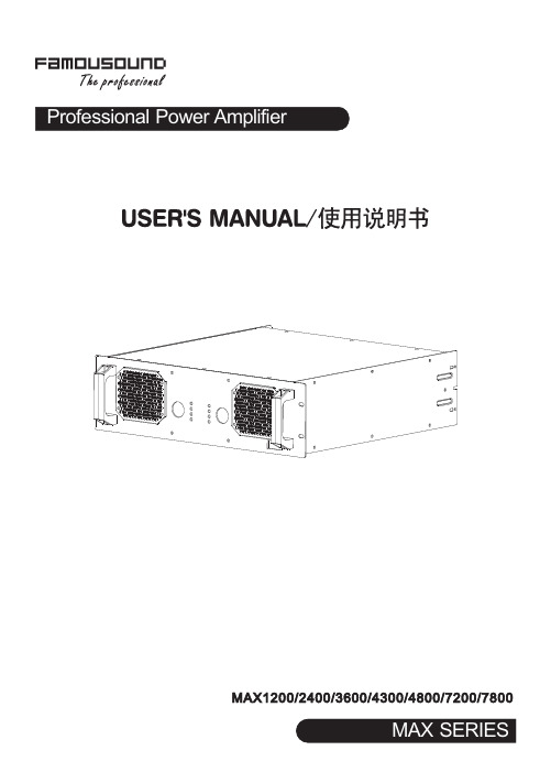
5. 安装孔 用于安装到机柜时固定用。
6. 通道1的音量控制器 功放工作于立体声或并接模式时由此控制器控制通道1的输出电平,功放工作于桥接模式时由此控制器控 制输出电平,此时通道2的音量控制器失效。
7. 保护指示 当此指示灯亮,处于保护状态,方便找出问题所在。 指示的保护功能有:削峰压限保护、过热保护、过载保护、短路保护、直流保护功能。
11电压增益频率响应总谐波失真转换速率阻尼系数动态范围信噪比输入灵敏度输入阻抗平衡不平衡输出级电路类型保护功能高通滤波器低通滤波器散热气流方向输入电压频率外箱尺寸mm重量压限直流短路开关机零冲击开机软启动vhf甚高频保护压限直流短路开关机零冲击开机软启动从功放面板进风23kg29kg29kg33kg35kg38kg33kgl620xw585xh210max1200max2400max3600max4300max7200max7800650wx21250wx2450wx2675wx2800wx2975wx21650wx21950wx2520wx2450wx2300wx21100wx2max4800830wx21250wx2900w1350w1600w1950w3300w3900w2500w620wx21000wx21200wx21400wx22160wx22700wx21850wx2桥接功率1240w2000w2400w2800w43200w5400w3700wmax系列技术参数12注意
2. TRS输入座(平衡或不平衡)。连接到上一级的周边处理设备。 3. 直通插座
与XLR 输入并联,提供一个与输入信号一样的输出信号,用此平衡插座连接到另一台设备。 (仅限于MAX4300、MAX4800、MAX7200、MAX7800) 4. 输入灵敏度开关 此开关用于选择功放的输入灵敏度:0.775V、1.0V及1.4V。(仅限于MAX4300、MAX4800、MAX7200、 MAX7800)。 5. 工作模式选择开关 用此开关去选择功放的工作模式: STEREO/立体声:两个通道完全独立。 PARALLEL/并接:信号共用通道1输入,音量独立控制,输出独立。 BRIDGE/桥接:信号共用通道1输入,音量由通道1控制,输出接通道1的SPEAKON。当使用到该工作模式 时,背板的指示灯亮。 注意:具体见下页的接线图。 6. 150Hz低通滤波器开关 若系统中需要推动超低音的音箱时,将开关拨到“ON”的位置可以滤掉150Hz以上的信号,直接使用功放 推动超低音的音箱,无需外加电子分频器。(仅限于MAX4300、MAX4800、MAX7200、MAX7800) 7. 音箱螺旋座输出 这是功放螺旋座的输出端。1+接喇叭的正端,1-接喇叭的负端,桥接时1+接喇叭的正端、2+接喇叭的负端。 8. 喇叭接线柱输出 这是功放喇叭接线柱的输出端。红色接喇叭的正端,黑色接喇叭的负端,桥接时只使用红色接喇叭的正端。 9. 保险管座 此保险管座内装由标准规格的保险管,用于故障时保护功放,如果功放已经接上电源待机指示灯没有点亮 时,请检查保险管的情况,如发现保险管已熔掉,在故障排除后,必须更换同一规格的保险管。 10. 散热的气流入口,不要有任何东西堵住。
MAX465中文资料

PART
DESCRIPΒιβλιοθήκη IONMAX463 MAX464 MAX465 MAX466 MAX467 MAX468 MAX469 MAX470
Triple RGB Switch & Buffer Quad RGB Switch & Buffer Triple RGB Switch & Buffer Quad RGB Switch & Buffer Triple Video Buffer Quad Video Buffer Triple Video Buffer Quad Video Buffer
Continuous Power Dissipation (TA = +70°C) 16-Pin Plastic DIP (derate 22.22mW/°C above +70°C) ....1778mW 16-Pin Wide SO (derate 20.00mW/°C above +70°C) .......1600mW
The MAX463–MAX470 series of two-channel, triple/quad buffered video switches and video buffers combines high-accuracy, unity-gain-stable amplifiers with high-performance video switches. Fast switching time and low differential gain and phase error make this series of switches and buffers ideal for all video applications. The devices are all specified for ±5V supply operation with inputs and outputs as high as ±2.5V when driving 150Ω loads (75Ω back-terminated cable).
MAX6373KA+T中文资料

General DescriptionThe MAX6369–MAX6374 are pin-selectable watchdog timers that supervise microprocessor (µP) activity and signal when a system is operating improperly. During normal operation, the microprocessor should repeated-ly toggle the watchdog input (WDI) before the selected watchdog timeout period elapses to demonstrate that the system is processing code properly. If the µP does not provide a valid watchdog input transition before the timeout period expires, the supervisor asserts a watch-dog (WDO ) output to signal that the system is not exe-cuting the desired instructions within the expected time frame. The watchdog output pulse can be used to reset the µP or interrupt the system to warn of processing errors.The MAX6369–MAX6374 are flexible watchdog timer supervisors that can increase system reliability through notification of code execution errors. The family offers several pin-selectable watchdog timing options to match a wide range of system timing applications:•Watchdog startup delay: provides an initial delay before the watchdog timer is started.•Watchdog timeout period: normal operating watch-dog timeout period after the initial startup delay.•Watchdog output/timing options: open drain (100ms)or push-pull (1ms).The MAX6369–MAX6374 operate over a +2.5V to +5.5V supply range and are available in miniature 8-pin SOT23 packages.________________________ApplicationsEmbedded Control Systems Industrial ControllersCritical µP and Microcontroller (µC) Monitoring AutomotiveTelecommunications NetworkingFeatures♦Precision Watchdog Timer for Critical µP Applications ♦Pin-Selectable Watchdog Timeout Periods ♦Pin-Selectable Watchdog Startup Delay Periods ♦Ability to Change Watchdog Timing Characteristics Without Power Cycling ♦Open-Drain or Push-Pull Pulsed Active-Low Watchdog Output ♦Watchdog Timer Disable Feature ♦+2.5V to +5.5V Operating Voltage ♦8µA Low Supply Current♦No External Components Required ♦Miniature 8-Pin SOT23 PackageMAX6369–MAX6374Pin-Selectable Watchdog Timers19-1676; Rev 3; 11/05Ordering InformationPin Configuration appears at end of data sheet.Note:All devices are available in tape-and-reel only. Required order increment is 2,500 pieces.Devices are available in both leaded and lead-free packaging.Specify lead-free by replacing “-T” with “+T” when ordering.Selector GuideFor pricing, delivery, and ordering information,please contact Maxim/Dallas Direct!at1-888-629-4642, or visit Maxim’s website at .M A X 6369–M A X 6374Pin-Selectable Watchdog Timers 2_______________________________________________________________________________________ABSOLUTE MAXIMUM RATINGSELECTRICAL CHARACTERISTICS(V CC = +2.5V to +5.5V, SET_ = V CC or GND, T A = -40°C to +85°C, unless otherwise noted. Typical values are at T A = +25°C andStresses beyond those listed under “Absolute Maximum Ratings” may cause permanent damage to the device. These are stress ratings only, and functional operation of the device at these or any other conditions beyond those indicated in the operational sections of the specifications is not implied. Exposure to absolute maximum rating conditions for extended periods may affect device reliability.Terminal Voltage (with respect to GND)V CC .....................................................................-0.3V to +6V WDI.....................................................................-0.3V to +6V WDO (Open Drain: MAX6369/71/73).................-0.3V to +6V WDO (Push-Pull: MAX6370/72/74 .......-0.3V to (V CC + 0.3V)SET0, SET1, SET2................................-0.3V to (V CC + 0.3V)Maximum Current, Any Pin (input/output)...........................20mAContinuous Power Dissipation (T A = +70°C)SOT23-8 (derate 8.75mW/°C above +70°C)...............700mW Operating Temperature Range ...........................-40°C to +85°C Storage Temperature Range.............................-65°C to +150°C Junction Temperature......................................................+150°C Lead Temperature (soldering, 10s).................................+300°C V CC Rise or Fall Rate......................................................0.05V/µsMAX6369–MAX6374Pin-Selectable Watchdog Timers_______________________________________________________________________________________3ELECTRICAL CHARACTERISTICS (continued)M A X 6369–M A X 6374Pin-Selectable Watchdog Timers 4_______________________________________________________________________________________461081214-4010-15356085SUPPLY CURRENT vs. TEMPERATURETEMPERATURE (°C)S U P P L Y C U R R E N T (µA )Typical Operating Characteristics(Circuit of Figure 1, T A = +25°C, unless otherwise noted .)0.9970.9990.9981.0011.0001.0021.003-4010-15356085WATCHDOG TIMEOUT PERIODvs. TEMPERATUREM A X 6369/74-02TEMPERATURE (°C)N O R M A L I Z E D W A T C H D O G T I M E O U T P E R I O DELECTRICAL CHARACTERISTICS (continued)Note 2:Guaranteed by design.Note 3:In this setting the watchdog timer is inactive and startup delay ends when WDI sees its first level transition. See SelectingDevice Timing for more information.Note 4:After power-up, or a setting change, there is an internal setup time during which WDI is ignored.MAX6369–MAX6374Pin-Selectable Watchdog Timers_______________________________________________________________________________________5Pin DescriptionDetailed DescriptionThe MAX6369–MAX6374 are flexible watchdog circuits for monitoring µP activity. During normal operation, the internal timer is cleared each time the µP toggles the WDI with a valid logic transition (low to high or high to low) within the selected timeout period (t WD ). The WDO remains high as long as the input is strobed within the selected timeout period. If the input is not strobed before the timeout period expires, the watchdog output is asserted low for the watchdog output pulse width (t WDO ). The device type and the state of the three logic control pins (SET0, SET1, and SET2) determine watch-dog timing characteristics. The three basic timing varia-tions for the watchdog startup delay and the normalTable 1 for the timeout characteristics for all devices in the family):•Watchdog Startup Delay:Provides an initial delay before the watchdog timer is started.Allows time for the µP system to power up and initial-ize before assuming responsibility for normal watch-dog timer updates.Includes several fixed or pin-selectable startup delay options from 200µs to 60s, and an option to wait for the first watchdog input transition before starting the watchdog timer.M A X 6369–M A X 6374Pin-Selectable Watchdog Timers 6_______________________________________________________________________________________•Watchdog Timeout Period:Normal operating watchdog timeout period after the initial startup delay.A watchdog output pulse is asserted if a valid watch-dog input transition is not received before the timeout period elapses.Eight pin-selectable timeout period options for each device, from 30µs to 60s.Pin-selectable watchdog timer disable feature.•Watchdog Output/Timing Options:Open drain, active low with 100ms minimum watch-dog output pulse (MAX6369/MAX6371/MAX6373).Push-pull, active low with 1ms minimum watchdog output pulse (MAX6370/MAX6372/MAX6374).Each device has a watchdog startup delay that is initi-ated when the supervisor is first powered or after the user modifies any of the logic control set inputs. The watchdog timer does not begin to count down until theFigure 1. Functional Diagramcompletion of the startup delay period, and no watch-dog output pulses are asserted during the startup delay. When the startup delay expires, the watchdog begins counting its normal watchdog timeout period and waiting for WDI transitions. The startup delay allows time for the µP system to power up and fully ini-tialize before assuming responsibility for the normal watchdog timer updates. Startup delay periods vary between the different devices and may be altered by the logic control set pins. To ensure that the system generates no undesired watchdog outputs, the routine watchdog input transitions should begin before the selected minimum startup delay period has expired. The normal watchdog timeout period countdown is initi-ated when the startup delay is complete. If a valid logic transition is not recognized at WDI before the watchdog timeout period has expired, the supervisor asserts a watchdog output. Watchdog timeout periods vary between the different devices and may be altered by the logic control set pins. To ensure that the system generates no undesired watchdog outputs, the watch-dog input transitions should occur before the selected minimum watchdog timeout period has expired.The startup delay and the watchdog timeout period are determined by the states of the SET0, SET1, and SET2 pins, and by the particular device within the family. For the MAX6369 and MAX6370, the startup delay is equal to the watchdog timeout period. The startup and watchdog timeout periods are pin selectable from 1ms to 60s (minimum).For the MAX6371 and MAX6372, the startup delay is fixed at 60s and the watchdog timeout period is pin selectable from 1ms to 60s (minimum).The MAX6373/MAX6374 provide two timing variations for the startup delay and normal watchdog timeout. Five of the pin-selectable modes provide startup delays from 200µs to 60s minimum, and watchdog timeout delays from 3ms to 10s minimum. Two of the selectable modes do not initiate the watchdog timer until the device receives its first valid watchdog input transition (there is no fixed period by which the first input must be received). These two extended startup delay modesare useful for applications requiring more than 60s for system initialization.All the MAX6369–MAX6374 devices may be disabledwith the proper logic control pin setting (Table 1).Applications InformationInput Signal Considerations Watchdog timing is measured from the last WDI risingor falling edge associated with a pulse of at least 100nsin width. WDI transitions are ignored when WDO is asserted, and during the startup delay period (Figure2). Watchdog input transitions are also ignored for asetup period, t SETUP, of up to 300µs after power-up ora setting change (Figure 3).Selecting Device TimingSET2, SET1, and SET0 program the startup delay and watchdog timeout periods (Table 1). Timeout settingscan be hard wired, or they can be controlled with logicgates and modified during operation. To ensure smooth transitions, the system should strobe WDI immediately before the timing settings are changed. This minimizesthe risk of initializing a setting change too late in thetimer countdown period and generating undesired watchdog outputs. After changing the timing settings,two outcomes are possible based on WDO. If the change is made while WDO is asserted, the previous setting is allowed to finish, the characteristics of thenew setting are assumed, and the new startup phase is entered after a 300µs setup time (t SETUP) elapses. Ifthe change is made while WDO is not asserted, thenew setting is initiated immediately, and the new start-up phase is entered after the 300µs setup time elapses.MAX6369–MAX6374Pin-Selectable Watchdog Timers_______________________________________________________________________________________7 Figure 3. Setting Change TimingM A X 6369–M A X 6374Pin-Selectable Watchdog TimersSelecting 011 (SET2 = 0, SET1 = 1, SET0 = 1) disables the watchdog timer function on all devices in the family.Operation can be reenabled without powering down by changing the set inputs to the new desired setting. The device assumes the new selected timing characteris-tics and enter the startup phase after the 300µs setup time elapses (Figure 3).The MAX6373/MAX6374 offer a first-edge feature. In first-edge mode (settings 101 or 110, Table 1), the internal timer does not control the startup delay period.Instead, startup terminates when WDI sees a transition.If changing to first-edge mode while the device is oper-ating, disable mode must be entered first. It is then safe to select first-edge mode. Entering disable mode first ensures the output is unasserted when selecting first-edge mode and removes the danger of WDI being masked out.OutputThe MAX6369/MAX6371/MAX6373 have an active-low,open-drain output that provides a watchdog output pulse of 100ms. This output structure sinks current when WDO is asserted. Connect a pullup resistor from WDO to any supply voltage up to +5.5V.Select a resistor value large enough to register a logic low (see Ele ctrical Characte ristics ), and small enoughto register a logic high while supplying all input current and leakage paths connected to the WDO line. A 10k Ωpullup is sufficient in most applications. The MAX6370/MAX6372/MAX6374 have push-pull outputs that pro-vide an active-low watchdog output pulse of 1ms.When WDO deasserts, timing begins again at the beginning of the watchdog timeout period (Figure 2).Usage in Noisy EnvironmentsIf using the watchdog timer in an electrically noisy envi-ronment, a bypass capacitor of 0.1µF should be con-nected between V CC and GND as close to the device as possible, and no further away than 0.2 inches.________________Watchdog SoftwareConsiderationsTo help the watchdog timer monitor software execution more closely, set and reset the watchdog input at differ-ent points in the program, rather than pulsing the watch-dog input high-low-high or low-high-low. This technique avoids a stuck loop, in which the watchdog timer would continue to be reset inside the loop, keeping the watch-dog from timing out. Figure 4 shows an example of a flow diagram where the I/O driving the watchdog input is set high at the beginning of the program, set low at the end of every subroutine or loop, then set high again when the program returns to the beginning. If the pro-gram should hang in any subroutine, the problem would be quickly corrected, since the I/O is continually set low and the watchdog timer is allowed to time out, causing WDO to pulse.Figure 4. Watchdog Flow DiagramChip InformationTRANSISTOR COUNT: 1500PROCESS: BiCMOSPin ConfigurationMaxim cannot assume re sponsibility for use of any circuitry othe r than circuitry e ntire ly e mbodie d in a Maxim product. No circuit pate nt lice nse s are implied. Maxim reserves the right to change the circuitry and specifications without notice at any time.8_____________________Maxim Integrated Products, 120 San Gabriel Drive, Sunnyvale, CA 94086 408-737-7600©2005 Maxim Integrated ProductsPrinted USAis a registered trademark of Maxim Integrated Products, Inc.。
max24033emy+t的规格书
max24033emy+t的规格书规格书:max24033emy+t一、产品介绍:max24033emy+t是一款高度集成的4通道电源管理IC,它主要用于工业控制系统、通信设备和数据中心等领域的电源管理。
该产品采用优质的半导体材料和先进的封装工艺,具有稳定可靠的性能和高效省电的特点。
二、产品特点:1.高度集成:max24033emy+t集成了4个高性能电源管理通道,包括电池充电管理、DC-DC转换器和电源监控等功能,可满足多种应用的需求。
2.宽输入电压范围:max24033emy+t支持广泛的输入电压范围,从3.5V到28V,能适应不同电源供应的要求。
3.高效节能:max24033emy+t采用了先进的能量管理技术,具有高效节能的特点,可以最大程度地减少能源浪费。
4.低功耗待机模式:max24033emy+t在待机模式下,功耗极低,能有效延长电池使用寿命。
5.温度保护:max24033emy+t具有自动温度保护功能,可在过热时自动停止工作,保护电路不受损坏。
6.电池管理:max24033emy+t支持电池充电和放电管理,能确保电池使用的安全和稳定性。
三、应用领域:max24033emy+t广泛应用于各种工业控制系统、通信设备和数据中心等领域,如智能家居、自动化控制、无线通信设备、数据存储等。
四、主要性能参数:1.输入电压范围:3.5V-28V2.输出电压范围:1.5V-16V3.输出电流范围:0A-3A4.工作温度范围:-40℃~85℃5.封装形式:QFN封装五、产品优势:1.优质材料:max24033emy+t采用优质的半导体材料和先进的封装工艺,保证了产品的稳定性和可靠性。
2.高效节能:max24033emy+t采用了先进的能量管理技术,具有高效节能的特点,能最大程度地减少能源浪费。
3.宽电压范围:max24033emy+t支持广泛的输入电压范围,能适应不同电源供应的要求。
4.多通道设计:max24033emy+t具有4个独立的电源管理通道,可满足多种应用的需求。
- 1、下载文档前请自行甄别文档内容的完整性,平台不提供额外的编辑、内容补充、找答案等附加服务。
- 2、"仅部分预览"的文档,不可在线预览部分如存在完整性等问题,可反馈申请退款(可完整预览的文档不适用该条件!)。
- 3、如文档侵犯您的权益,请联系客服反馈,我们会尽快为您处理(人工客服工作时间:9:00-18:30)。
General Description The MAX6381–MAX6390 microprocessor (µP) supervisory circuits monitor power-supply voltages from +1.8V to +5.0V while consuming only 3µA of supply current at +1.8V. Whenever V CC falls below the factory-set reset thresholds, the reset output asserts and remains assert-ed for a minimum reset timeout period after V CC rises above the reset threshold. Reset thresholds are available from +1.58V to +4.63V, in approximately 100mV incre-ments. Seven minimum reset timeout delays ranging from 1ms to 1200ms are available.The MAX6381/MAX6384/MAX6387 have a push-pull active-low reset output. The MAX6382/MAX6385/ MAX6388 have a push-pull active-high reset output, and the MAX6383/MAX6386/MAX6389/MAX6390 have an open-drain active-low reset output. The MAX6384/MAX6385/MAX6386 also feature a debounced manual reset input (with internal pullup resistor). The MAX6387/MAX6388/MAX6389 have an auxiliary input for monitoring a second voltage. The MAX6390 offers a manual reset input with a longer V CC reset timeout period (1120ms or 1200ms) and a shorter manual reset timeout (140ms or 150ms).The MAX6381/MAX6382/MAX6383 are available in 3-pin SC70 and6-pinµDFN packages and the MAX6384–MAX6390 are available in 4-pin SC70 andFeatures♦Factory-Set Reset Threshold Voltages Rangingfrom +1.58V to +4.63V in Approximately 100mVIncrements♦±2.5% Reset Threshold Accuracy OverTemperature (-40°C to +125°C)♦Seven Reset Timeout Periods Available: 1ms,20ms, 140ms, 280ms, 560ms, 1120ms,1200ms (min)♦3 Reset Output OptionsActive-Low Push-PullActive-High Push-PullActive-Low Open-Drain♦Reset Output State Guaranteed ValidDown to V CC= 1V♦Manual Reset Input (MAX6384/MAX6385/MAX6386)♦Auxiliary RESET IN(MAX6387/MAX6388/MAX6389)♦V CC Reset Timeout (1120ms or 1200ms)/ManualReset Timeout (140ms or 150ms) (MAX6390)♦Negative-Going V CC Transient Immunity♦Low Power Consumption of 6µA at +3.6Vand 3µA at +1.8V♦Pin Compatible withMAX809/MAX810/MAX803/MAX6326/MAX6327/MAX6328/MAX6346/MAX6347/MAX6348,and MAX6711/MAX6712/MAX6713♦Tiny 3-Pin/4-Pin SC70 and 6-Pin µDFN PackagesMAX6381–MAX6390 SC70/µDFN, Single/Dual Low-Voltage,Low-Power µP Reset Circuits ________________________________________________________________Maxim Integrated Products1Pin Configurations19-1839; Rev 4; 4/07Ordering InformationOrdering Information continued at end of data sheet.Typi cal Operati ng Ci rcui t appears at end of data sheet.Selector Guide appears at end of data sheet.after "XR", "XS", or "LT." Insert reset timeout delay (see ResetTimeout Delay table) after "D" to complete the part number.Sample stock is generally held on standard versions only (seeStandard Versions table). Standard versions have an orderincrement requirement of 2500 pieces. Nonstandard versionshave an order increment requirement of 10,000 pieces.Contact factory for availability of nonstandard versions.+Denotes a lead-free package.For pricing, delivery, and ordering information,please contact Maxim Direct at 1-888-629-4642,or visit Maxim’s website at .ComputersControllersIntelligent InstrumentsCritical µP and µCPower MonitoringPortable/Battery-Powered EquipmentDual Voltage SystemsM A X 6381–M A X 6390SC70/µDFN, Single/Dual Low-Voltage, Low-Power µP Reset CircuitsABSOLUTE MAXIMUM RATINGSELECTRICAL CHARACTERISTICS(V CC = full range, T A = -40°C to +125°C, unless otherwise specified. Typical values are at T A = +25°C.) (Note 1)Stresses beyond those listed under “Absolute Maximum Ratings” may cause permanent damage to the device. These are stress ratings only, and functional operation of the device at these or any other conditions beyond those indicated in the operational sections of the specifications is not implied. Exposure to absolute maximum rating conditions for extended periods may affect device reliability.V CC to GND..........................................................-0.3V to +6.0V RESET Open-Drain Output....................................-0.3V to +6.0V RESET , RESET (push-pull output)..............-0.3V to (V CC + 0.3V)MR , RESET IN.............................................-0.3V to (V CC + 0.3V)Input Current (V CC ).............................................................20mA Output Current (all pins).....................................................20mAContinuous Power Dissipation (T A = +70°C)3-Pin SC70 (derate 2.9mW/°C above +70°C)..............235mW 4-Pin SC70 (derate 3.1mW/°C above +70°C)..............245mW 6-Pin µDFN (derate 2.1mW/°C above +70°C)..........167.7mW Operating Temperature Range .........................-40°C to +125°C Storage Temperature Range.............................-65°C to +150°C Lead Temperature (soldering, 10s).................................+300°CMAX6381–MAX6390SC70/µDFN, Single/Dual Low-Voltage,Low-Power µP Reset Circuits_______________________________________________________________________________________3M A X 6381–M A X 6390SC70/µDFN, Single/Dual Low-Voltage, Low-Power µP Reset Circuits 4______________________________________________________________________________________Typical Operating Characteristics(T A = +25°C, unless otherwise noted.)215436789-40-105-25203550658095110125SUPPLY CURRENT vs. TEMPERATURE(NO LOAD)TEMPERATURE (°C)S U P P L Y C U R R E N T (µA )25292735333137394143-40-105-25203550658095110125POWER-DOWN RESET DELAYvs. TEMPERATURETEMPERATURE (°C)P O W E R -D O W N R E S E T D E L A Y (µs )0.940.980.961.021.001.061.041.08-40-10520-253550658095110125NORMALIZED POWER-UP RESET TIMEOUTvs. TEMPERATUREM A X 6381/90 t o c 03TEMPERATURE (°C)N O R M A L I Z E D R E S E T T I M E O U T P E R I O D0.9900.9851.0150.9950.9901.0001.0051.0101.020-40-10520-253550958011065125M A X 6381/90 t o c 04TEMPERATURE (°C)N O R M A L I Z E D R E S E T TH R E S H O L D NORMALIZED RESET THRESHOLDvs. TEMPERATURE00.40.20.80.61.01.2063912OUTPUT-VOLTAGE LOW vs. SINK CURRENTI SINK (mA)V O L (V )01.00.52.01.52.53.00500750250100012501500OUTPUT-VOLTAGE HIGH vs. SOURCE CURRENTI SOURCE (µA)V O H (V )45001100010010MAXIMUM TRANSIENT DURATION vs. RESET COMPARATOR OVERDRIVE15050350250500200100400300RESET COMPARATOR OVERDRIVE, V TH - V CC (mV)M A X I M U M T R A N S I E N T D U R A T I O N (µs )3.53.93.74.54.34.14.74.95.35.15.5-40-105-25203550658095110125RESET IN TO RESET DELAYvs. TEMPERATUREM A X 6381/90 t o c 08TEMPERATURE (°C)R E S E T I N D E L A Y (µs )MAX6381–MAX6390SC70/µDFN, Single/Dual Low-Voltage,Low-Power µP Reset CircuitsPin DescriptionM A X 6381–M A X 6390SC70/µDFN, Single/Dual Low-Voltage, Low-Power µP Reset Circuits 6_______________________________________________________________________________________Detailed DescriptionRESET OutputA µP reset input starts the µP in a known state. These µP supervisory circuits assert reset to prevent code execution errors during power-up, power-down, or brownout conditions.Reset asserts when V CC is below the reset threshold;once V CC exceeds the reset threshold, an internal timer keeps the reset output asserted for the reset timeout period. After this interval, reset output deasserts. Reset output is guaranteed to be in the correct logic state for V CC ≥1V.Manual Reset Input (MAX6384/MAX6385/MAX6386/MAX6390)Many µP-based products require manual reset capabil-ity, allowing the operator, a test technician, or external logic circuitry to initiate a reset. A logic low on MR asserts reset. Reset remains asserted while MR is low,and for the reset active timeout period (t RP ) after MR returns high. This input has an internal 63k Ωpullup resistor (1.56k Ωfor MAX6390), so it can be left uncon-nected if it is not used. MR can be driven with TTL or CMOS logic levels, or with open-drain/collector outputs.Connect a normally open momentary switch from MR to G ND to create a manual-reset function; external debounce circuitry is not required. If MR is driven from long cables or if the device is used in a noisy environ-ment, connecting a 0.1µF capacitor from MR to G ND provides additional noise immunity.RESET IN Comparator(MAX6387/MAX6388/MAX6389)RESET IN is compared to an internal +1.27V reference.If the voltage at RESET IN is less than 1.27V, reset asserts. Use the RESET IN comparator as a user-adjustable reset detector or as a secondary power-sup-ply monitor by implementing a resistor-divider at RESET IN (shown in Figure 1). Reset asserts when either V CC or RESET IN falls below its respective threshold volt-age. Use the following equation to set the threshold:V INTH = V THRST (R1/R2 + 1)where V THRST = +1.27V. To simplify the resistor selec-tion, choose a value of R2 and calculate R1:R1 = R2 [(V INTH /V THRST ) - 1]Since the input current at RESET IN is 50nA (max),large values can be used for R2 with no significant loss in accuracy.___________Applications InformationNegative-Going V CC TransientsIn addition to issuing a reset to the µP during power-up,power-down, and brownout conditions, the MAX6381–MAX6390 are relatively immune to short dura-tion negative-going V CC transients (glitches).The Typical Operating Characteristics section shows the Maximum Transient Durations vs. Reset Comparator Overdrive, for which the MAX6381–MAX6390 do not generate a reset pulse. This graph was generated usinga negative-going pulse applied to V CC , starting above the actual reset threshold and ending below it by the magnitude indicated (reset comparator overdrive). The graph indicates the typical maximum pulse width a neg-ative-going V CC transient may have without causing a reset pulse to be issued. As the magnitude of the tran-sient increases (goes farther below the reset threshold),the maximum allowable pulse width decreases. A 0.1µF capacitor mounted as close as possible to V CC provides additional transient immunity.Ensuring a Valid RESET Output Down to V CC = 0VThe MAX6381–MAX6390 are guaranteed to operate properly down to V CC = 1V. In applications that require valid reset levels down to V CC = 0V, a pulldown resistor to active-low outputs (push/pull only, Figure 2) and a pullup resistor to active-high outputs (push/pull only)will ensure that the reset line is valid while the reset out-put can no longer sink or source current. This schemedoes not work with the open-drain outputs of the MAX6383/MAX6386/MAX6389/MAX6390. The resistor value used is not critical, but it must be small enough not to load the reset output when V CC is above the reset threshold. For most applications, 100k Ωis ade-quate.MAX6381–MAX6390SC70/µDFN, Single/Dual Low-Voltage,Low-Power µP Reset Circuits_______________________________________________________________________________________7M A X 6381–M A X 6390SC70/µDFN, Single/Dual Low-Voltage, Low-Power µP Reset Circuits 8_______________________________________________________________________________________Selector GuideOrdering Information (continued)Note:Insert reset threshold suffix (see Reset Threshold table)after "XR", "XS", or "LT." Insert reset timeout delay (see Reset Timeout Delay table) after "D" to complete the part number.Sample stock is generally held on standard versions only (see Standard Versions table). Standard versions have an order increment requirement of 2500 pieces. Nonstandard versions have an order increment requirement of 10,000 pieces.Contact factory for availability of nonstandard versions.*MAX6390 is available with D4 or D7 timing only.+Denotes a lead-free package.MAX6381–MAX6390SC70/µDFN, Single/Dual Low-Voltage,Low-Power µP Reset Circuits_______________________________________________________________________________________9Chip InformationTRANSISTOR COUNT: 647PROCESS: BiCMOSPin Configurations (continued)M A X 6381–M A X 6390SC70/µDFN, Single/Dual Low-Voltage, Low-Power µP Reset Circuits 10______________________________________________________________________________________Package Information(The package drawing(s) in this data sheet may not reflect the most current specifications. For the latest package outline information,go to /packages .)MAX6381–MAX6390SC70/µDFN, Single/Dual Low-Voltage,Low-Power µP Reset Circuits______________________________________________________________________________________11Package Information (continued)(The package drawing(s) in this data sheet may not reflect the most current specifications. For the latest package outline information,go to /packages .)M A X 6381–M A X 6390SC70/µDFN, Single/Dual Low-Voltage, Low-Power µP Reset Circuits 12______________________________________________________________________________________Package Information (continued)(The package drawing(s) in this data sheet may not reflect the most current specifications. For the latest package outline information,go to /packages .)SC70/µDFN, Single/Dual Low-Voltage,Low-Power µP Reset CircuitsMaxim cannot assume responsibility for use of any circuitry other than circuitry entirely embodied in a Maxim product. No circuit patent licenses are implied. Maxim reserves the right to change the circuitry and specifications without notice at any time.Maxim Integrated Products, 120 San Gabriel Drive, Sunnyvale, CA 94086 408-737-7600____________________13©2007 Maxim Integrated Productsis a registered trademark of Maxim Integrated Products, Inc.MAX6381–MAX6390Package Information (continued)(The package drawing(s) in this data sheet may not reflect the most current specifications. For the latest package outline information,go to /packages .)Revision HistoryPages changed at Rev 4: Title on all pages, 1, 2, 5,7–13。