T835-400B中文资料
T810-XXXB中文资料

ITSM(A) 80 70 60 50 40 30 20 10
0 1
Tj initial=25°C F=50Hz
Number of cycles
10
100
1000
Fig 7: Non repetitive surge peak on-state current for a sinusoidal pulse with width tp<10ms, and corresponding value of I2t.
Symbol
Test Conditions
Quadrant
IGT VGT VGD IL IH * VTM * IDRM IRRM
VD=12V (DC) RL=33Ω VD=12V (DC) RL=33Ω VD=VDRM RL=3.3kΩ IG=1.2 IGT IT= 100mA gate open ITM= 11A tp= 380µs VDRM Rated VRRM Rated
0
0
1
2
3
4
5
6
7
8
Fig 2: Correlation between maximum power dissipation and maximum allowable temperatures (Tamb and Tcase) for different thermal resistances heatsink+contact.
260
Unit A A
A2s A/µs
°C °C °C
Symbol
Parameter
VDRM VRRM
Repetitive peak off-state voltage Tj = 125 °C
中国赛宝 420B型 说明书

使用说明书 User’s Manual420B 型接触电流测试仪校验及校正声明本实验室特别声明,本手册所列的仪器设备完全符合本实验室一般目录上所标称的规范和特性。
本仪器在出厂前已经通过本实验室厂内校验,校验的程序和步骤是符合电子检验中心的规范和标准。
产品品质保证本实验室保证所生产制造的新品仪器均经过严格的品质确认,同时保证在出厂一年内,如有发现产品的施工瑕疵或零件故障,本实验室负责免费给予修复。
但是如果使用者有自行更改电路、功能、或进行修理仪器及零件或外箱损坏等情况,本实验室恕不提供免费保修服务。
本保证不含本仪器的附属设备等非我实验室所生产的附件。
在一年的保修期内,请将故障机组送回本实验室设备研发部维修处,本实验室会予以妥善修护。
如果本机组在非正常的使用下、或人为疏忽、或非人力可控制下发生故障,例如地震、水灾、暴动、或火灾等非人力可控制的因素,本实验室不予免费保修服务。
(本实验室遵循可持续发展战略,保留对本说明书的内容进行改进不予先通知的权力)设备使用安全规定(必读)使用前应该注意的规定和事项!!!安全标志 :高电压警告符号。
高压危险符号。
机体接地符号。
接地符号1.1 安全须知·使用本电容器纹波试验台以前,请先了解本机所使用和相关的安全标志,以策安全.·在开启本机的输入电源开关前,请先选择正确的输入电压规格.为防止意外伤害或死亡发生,在搬移和使用机器时,请务必先观察清楚,然后再进行操作.1.2 维护和保养使用者的维护为了防止触电的发生,请不要掀开仪器的盖子。
本仪器内部所有的零件绝对不需使用者维护。
如果仪器有异常情况发生,请寻求我实验室给予维护。
所附的线路和方块图只供参考之用。
定期维护交流电源供应器、输入电源线各相关附件等每年至少要仔细检验和校验一次,以保护使用者的安全和仪器的精确性。
使用者的修改使用者不得自行更改机器的线路或零件,如被更改,机器保证期则自动失效并且我实验室不负责任。
832B中文资料
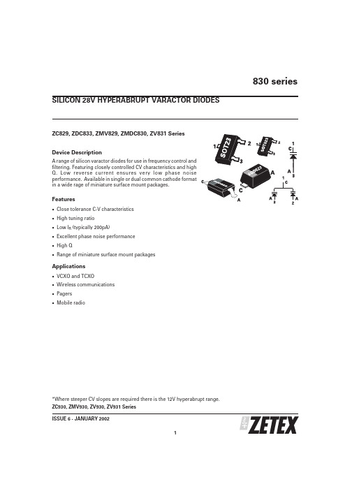
ZC829, ZDC833, ZMV829, ZMDC830, ZV831 Series Device DescriptionA range of silicon varactor diodes for use in frequency control and filtering.Featuring closely controlled CV characteristics and high Q.Low reverse current ensures very low phase noise performance.Available in single or dual common cathode format in a wide rage of miniature surface mount packages.Features·Close tolerance C-V characteristics ·High tuning ratio ·Low I R (typically 200pA)·Excellent phase noise performance ·High Q·Range of miniature surface mount packagesApplications·VCXO and TCXO·Wireless communications ·Pagers ·Mobile radio*Where steeper CV slopes are required there is the 12V hyperabrupt range.ZC930, ZMV930, ZV930, ZV931 Series 830 seriesISSUE 6 - JANUARY 20021SILICON 28V HYPERABRUPT VARACTOR DIODES830 seriesISSUE 6 - JANUARY 20022PARTCapacitance (pF)V R =2V,f=1MHzMin Q V R =3V f=50MHzCapacitance RatioC 2/C 20at f=1MHzMIN.NOM.MAX.MIN.MAX.829A 7.388.29.02250 4.3 5.8829B 7.798.28.61250 4.3 5.8830A 9.010.011.0300 4.5 6.0830B 9.510.010.5300 4.5 6.0831A 13.515.016.5300 4.5 6.0831B 14.2515.015.75300 4.5 6.0832A 19.822.024.2200 5.0 6.5832B 20.922.023.1200 5.0 6.5833A 29.733.036.3200 5.0 6.5833B 31.3533.034.65200 5.0 6.5834A 42.347.051.7200 5.0 6.5834B 44.6547.049.35200 5.0 6.5835A 61.268.074.8100 5.0 6.5835B 64.668.071.4100 5.0 6.5836A 90.0100.0110.0100 5.0 6.5836B95.0100.0105.0100 5.06.5TUNING CHARACTERISTICS at Tamb = 25°CPARAMETER SYMBOLMAX UNIT Forward currentI F 200mA Power dissipation at T amb =25ЊC SOT23P tot 330mW Power dissipation at T amb =25ЊC SOD323P tot 330mW Power dissipation at T amb =25ЊC SOD523P tot250mW Operating and storage temperature range-55to +150ЊCABSOLUTE MAXIMUM RATINGSPARAMETERCONDITIONS MIN.TYP.MAX.UNIT Reverse breakdown voltage I R =10uA 25V Reverse voltage leakageV R =20V 0.220nA Temperature coefficient of capacitanceV R =3V,f =1MHz300400ppCm/ЊCELECTRICAL CHARACTERISTICS at Tamb = 25°C830 seriesTYPICAL CHARACTERISTICSISSUE 6 - JANUARY 20023830 seriesISSUE 6 - JANUARY 20024O R D E R C O D E S A N D P A R T M A R K I N GR E E L C O D ER E E L S I Z ET A P E W I D T HQ U A N T I T Y P E R R E E LT A7i n c h (180m m )8m m3000T C13i n c h (330m m )8m m 10000T A P E A N D R E E L I N F O R M A T I O NT h e o r d e r c o d e s a r e s h o w n a s T A w h i c h i s f o r 7i n c h r e e l s .F o r 13i n c h r e e l s s u b s t i t u t e T C i n p l a c e o f T A i n t h e o r d e r c o d e .ISSUE 6 - JANUARY 20025830 seriesSOT23 PACKAGE DIMENSIONSSOD323 PACKAGE DIMENSIONSZetex plcFields New Road ChaddertonOldham, OL9 8NP United KingdomTelephone (44) 161 622 4422Fax: (44) 161 622 4420Zetex GmbHStreitfeldstraße 19D-81673 München GermanyTelefon: (49) 89 45 49 49 0Fax: (49) 89 45 49 49 49Zetex Inc700 Veterans Memorial Hwy Hauppauge, NY11788USATelephone: (631) 360 2222Fax: (631) 360 8222Zetex (Asia) Ltd3701-04Metroplaza, Tower 1Hing Fong Road Kwai Fong Hong KongTelephone: (852) 26100 611Fax: (852) 24250 494These offices are supported by agents and distributors in major countries world-wide.This publication is issued to provide outline information only which (unless agreed by the Company in writing)may not be used,applied or reproduced for any purpose or form part of any order or contract or be regarded as a representation relating to the products or services concerned.The Company reserves the right to alter without notice the specification,design,price or conditions of supply of any product or service.For the latest product information,log on to©Zetex plc 2001830 series6ISSUE 6 - JANUARY 2002DIM MILLIMETRES MIN.MAX A ᎏ0.800A10.0000.100A20.6000.800b10.1600.300c 0.0800.220D 0.7000.900E 1.500 1.700E1 1.100 1.300L 0.2000.400L10.1700.230⍜1Њ4Њ10ЊSOD523 PACKAGE DIMENSIONSSOD323 PACKAGE DIMENSIONS。
检波器测试仪手册编制-1

灵敏度 误差 精度 分辨率 % V/m/s ±2 ±2 ±4 ±2 ±2 ±2 ±2 ±2 ±1 ±1 ±1 0.01 0.01 0.01 0.1 0.1 ; 0.1 0.1 0.1 0~20 0~20 0~20 0~20 范围 % 0~20 0~20
谐波畸变 误差 精度% ±10 ±10 分辨 率% 范围 Ω
* : 表示检波器测试仪在自然频率<8Hz 时,误差精度±2% ;8Hz~14Hz时,误差精度 ±0.5%;>14Hz 时误差精度± 1% **: 表示检波器测试仪在自然频率 8~14 Hz,误差精度为±0.5 %;其他范围时,误差精度为±2%; ***:表示线圈电阻误差分辨率通常为1Ω ,若测量值低于100Ω 时,分辨率为0.1Ω 。
普通检波器 1~100 水中检波器 1~100
SGT-II SMT200 SMT300 SMT400 ZSF-300 TD2003 TD800 TD700 GT-7026A JCY150
1~100 1~100 1~100 5~100 8~100
±10 ±10 ±10 ±10
±1.0%± 0.01
20~24000 0.01 20~99999 0.01 20~200K
±0.01 ±0.01 ±0.01
0.01 0.01 0.01
20~200K 20~200K 20~200K
0.01 0.01 0.01 0.1
0.2~0.85 ≤0.7 0.001 0~500 ≤0.7 0.05~0.85 ±1 0.01 0~1000 ±2
≤0.02 0.001 100~99999 ≤0.7 0.01 20~9999 ±1
漏电测试 范围 Ω 0.1~10M 0.1~10M 0.1~10M 0.1~10M 1~100M 1~100M 1~100M 误差 精度 % ±10 ±10 ±10 ±10 ± 5 ± 5 ± 5 0.01 分辨率 MΩ
1N4003-B中文资料

Features1N4001/L - 1N4007/L1.0A RECTIFIERNo Suffix Designates DO-41 Package Maximum Ratings and Electrical Characteristics@ T A = 25°C unless otherwise specified·Diffused Junction·High Current Capability and Low Forward Voltage Drop ·Surge Overload Rating to 30A Peak ·Low Reverse Leakage Current·Lead Free Finish,RoHS Compliant (Note 4)Mechanical Data·Case: DO-41, A-405·Case Material: Molded Plastic. UL Flammability Classification Rating 94V-0·Moisture Sensitivity: Level 1 per J-STD-020C·Terminals: Finish - Bright Tin. Plated Leads Solderable per MIL-STD-202, Method 208·Polarity: Cathode Band ·Mounting Position: Any·Ordering Information: See Last Page ·Marking: Type Number·Weight: DO-41 0.30 grams (approximate)A-405 0.20 grams (approximate)Single phase, half wave, 60Hz, resistive or inductive load.For capacitive load, derate current by 20%.Notes: 1. Leads maintained at ambient temperature at a distance of 9.5mm from the case.2. Measured at 1. MHz and applied reverse voltage of 4.0V DC.3.JEDEC Value.4.RoHS revision 13.2.2003. Glass and High Temperature Solder Exemptions Applied, see EU Directive Annex Notes 5 and 7.4060801001201401601800.20.40.60.81.0I ,A V E R A G E F O R W A R D R E C T I F I E D C U R R E N T (A )(A V )T ,AMBIENT TEMPERATURE (ºC)Fig.1Forward Current Derating CurveA C ,C A P A C I T A N C E (p F )j V ,REVERSE VOLTAGE (V)Fig.4Typical Junction CapacitanceR 1.0101001.0101001.010100I ,P E A K F O R W A R D S U R G E C U R R E N T (A )F S M NUMBER OF CYCLES AT 60HzFig.3Max Non-Repetitive Peak FwdSurge Current403020010500.60.8 1.0 1.2 1.4 1.60.010.11.0I ,I N S T A N T A N E O U S F O R W A R D C U R R E N T (A )F V ,INSTANTANEOUSFORWARD VOLTAGE (V)Fig.2Typical Forward CharacteristicsF 10Ordering InformationNotes: 5. For packaging details, visit our website at /datasheets/ap02008.pdf(Note 5)IMPORTANT NOTICELIFE SUPPORTDiodes Incorporated and its subsidiaries reserve the right to make modifications,enhancements,improvements,corrections or other changes without further notice to any product herein.Diodes Incorporated does not assume any liability arising out of the application or use of any product described herein;neither does it convey any license under its patent rights,nor the rights of others.The user of products in such applications shall assume all risks of such use and will agree to hold Diodes Incorporated and all the companies whose products are represented on our website,harmless against all damages.Diodes Incorporated products are not authorized for use as critical components in life support devices or systems without the expressed written approval of the President of Diodes Incorporated.。
834B中文资料

ZC829, ZDC833, ZMV829, ZMDC830, ZV831 Series Device DescriptionA range of silicon varactor diodes for use in frequency control and filtering.Featuring closely controlled CV characteristics and high Q.Low reverse current ensures very low phase noise performance.Available in single or dual common cathode format in a wide rage of miniature surface mount packages.Features·Close tolerance C-V characteristics ·High tuning ratio ·Low I R (typically 200pA)·Excellent phase noise performance ·High Q·Range of miniature surface mount packagesApplications·VCXO and TCXO·Wireless communications ·Pagers ·Mobile radio*Where steeper CV slopes are required there is the 12V hyperabrupt range.ZC930, ZMV930, ZV930, ZV931 Series 830 seriesISSUE 6 - JANUARY 20021SILICON 28V HYPERABRUPT VARACTOR DIODES830 seriesISSUE 6 - JANUARY 20022PARTCapacitance (pF)V R =2V,f=1MHzMin Q V R =3V f=50MHzCapacitance RatioC 2/C 20at f=1MHzMIN.NOM.MAX.MIN.MAX.829A 7.388.29.02250 4.3 5.8829B 7.798.28.61250 4.3 5.8830A 9.010.011.0300 4.5 6.0830B 9.510.010.5300 4.5 6.0831A 13.515.016.5300 4.5 6.0831B 14.2515.015.75300 4.5 6.0832A 19.822.024.2200 5.0 6.5832B 20.922.023.1200 5.0 6.5833A 29.733.036.3200 5.0 6.5833B 31.3533.034.65200 5.0 6.5834A 42.347.051.7200 5.0 6.5834B 44.6547.049.35200 5.0 6.5835A 61.268.074.8100 5.0 6.5835B 64.668.071.4100 5.0 6.5836A 90.0100.0110.0100 5.0 6.5836B95.0100.0105.0100 5.06.5TUNING CHARACTERISTICS at Tamb = 25°CPARAMETER SYMBOLMAX UNIT Forward currentI F 200mA Power dissipation at T amb =25ЊC SOT23P tot 330mW Power dissipation at T amb =25ЊC SOD323P tot 330mW Power dissipation at T amb =25ЊC SOD523P tot250mW Operating and storage temperature range-55to +150ЊCABSOLUTE MAXIMUM RATINGSPARAMETERCONDITIONS MIN.TYP.MAX.UNIT Reverse breakdown voltage I R =10uA 25V Reverse voltage leakageV R =20V 0.220nA Temperature coefficient of capacitanceV R =3V,f =1MHz300400ppCm/ЊCELECTRICAL CHARACTERISTICS at Tamb = 25°C830 seriesTYPICAL CHARACTERISTICSISSUE 6 - JANUARY 20023830 seriesISSUE 6 - JANUARY 20024O R D E R C O D E S A N D P A R T M A R K I N GR E E L C O D ER E E L S I Z ET A P E W I D T HQ U A N T I T Y P E R R E E LT A7i n c h (180m m )8m m3000T C13i n c h (330m m )8m m 10000T A P E A N D R E E L I N F O R M A T I O NT h e o r d e r c o d e s a r e s h o w n a s T A w h i c h i s f o r 7i n c h r e e l s .F o r 13i n c h r e e l s s u b s t i t u t e T C i n p l a c e o f T A i n t h e o r d e r c o d e .ISSUE 6 - JANUARY 20025830 seriesSOT23 PACKAGE DIMENSIONSSOD323 PACKAGE DIMENSIONSZetex plcFields New Road ChaddertonOldham, OL9 8NP United KingdomTelephone (44) 161 622 4422Fax: (44) 161 622 4420Zetex GmbHStreitfeldstraße 19D-81673 München GermanyTelefon: (49) 89 45 49 49 0Fax: (49) 89 45 49 49 49Zetex Inc700 Veterans Memorial Hwy Hauppauge, NY11788USATelephone: (631) 360 2222Fax: (631) 360 8222Zetex (Asia) Ltd3701-04Metroplaza, Tower 1Hing Fong Road Kwai Fong Hong KongTelephone: (852) 26100 611Fax: (852) 24250 494These offices are supported by agents and distributors in major countries world-wide.This publication is issued to provide outline information only which (unless agreed by the Company in writing)may not be used,applied or reproduced for any purpose or form part of any order or contract or be regarded as a representation relating to the products or services concerned.The Company reserves the right to alter without notice the specification,design,price or conditions of supply of any product or service.For the latest product information,log on to©Zetex plc 2001830 series6ISSUE 6 - JANUARY 2002DIM MILLIMETRES MIN.MAX A ᎏ0.800A10.0000.100A20.6000.800b10.1600.300c 0.0800.220D 0.7000.900E 1.500 1.700E1 1.100 1.300L 0.2000.400L10.1700.230⍜1Њ4Њ10ЊSOD523 PACKAGE DIMENSIONSSOD323 PACKAGE DIMENSIONS。
ZXTP08400BFFTA;中文规格书,Datasheet资料

ZXTP08400BFF400V, SOT23F, PNP medium power high voltage transistorSummary;BV CEO > -400V BV ECO > -6V I C(cont) = -0.2AV CE(sat) < 220mV @ 100mA P D = 1.5WComplementary part number ZXTN08400BFFDescriptionThis PNP transistor has been designed for applications requiring high blocking voltage. The SOT23F package is pin compatible with the industry standard SOT23 footprint but offers lower profile and higher dissipation for applications where power density is of utmost importance.Features•High voltage•Low saturation voltageApplications•Telecoms switchingOrdering informationDevice marking1D6DeviceReel size (inches)Tape width (mm)Quantity per reel ZXTP08400BFFTA783000Absolute maximum ratingsParameter Symbol Limit Unit Collector-base voltage V CBO-400V Collector-emitter voltage V CEO-400V Emitter-collector voltage (reverse blocking)V ECO-6V Emitter-base voltage V EBO-7V Continuous collector current(c)I C-0.2A Peak pulse current I CM-1A Base current I B-0.2A Power dissipation at T amb =25°C(a)0.84W Linear derating factor P D 6.72mW/°C Power dissipation at T amb =25°C(b) 1.34W Linear derating factor P D10.72mW/°C Power dissipation at T amb =25°C(c) 1.50W Linear derating factor P D12.0mW/°C Power dissipation at T amb =25°C(d) 2.0W Linear derating factor P D16.0mW/°C Operating and storage temperature range T j, T stg -55 to 150°CThermal resistamceParameter Symbol Limit Unit Junction to ambient(a)R⍜JA149°C/W Junction to ambient(b)R⍜JA93°C/W Junction to ambient(c)R⍜JA83°C/W Junction to ambient(d)R⍜JA60°C/W NOTES:(a)For a device surface mounted on 15mm x 15mm x 1.6mm FR4 PCB with high coverage of single sided 1oz copper, instill air conditions.(b)Mounted on 25mm x 25mm x 1.6mm FR4 PCB with a high coverage of single sided 2 oz copper in still air conditions.(c)Mounted on 50mm x 50mm x 1.6mm FR4 PCB with a high coverage of single sided 2 oz copper in still air conditions.(d)As (c) above measured at t<5secs.CharacteristicsElectrical characteristics (at T amb = 25°C unless otherwise stated)ParameterSymbol Min.Typ.Max.Unit Conditions Collector-base breakdown voltageBV CBO-400-500V I C = -100A Collector-emitter breakdown voltage (base open)BV CEO -400-480V I C = -10mA (*) NOTES:(*)Measured under pulsed conditions. Pulse width Յ300s; duty cycle Յ2%.Emitter-base breakdown voltageBV EBO-7-8.1V I E = -100AEmitter-collector breakdown voltage (reverse blocking)BV ECX -6-8.2V I E = -100A, R BC < 1k ⍀ or 0.25V > V BC > -0.25V Emitter-collector breakdown voltage (base open)BV ECO -6-8.6V I E = -100A,Collector-base cut-off current I CBO <-1-50-20nA A V CB = -320VV CB = -320V, T amb = 100°C Emitter-base cut-off current I EBO <-1-50nA V EB = -5.6VCollector-emitter saturation voltageV CE(sat)-10-145mV I C = -20mA, I B = -1mA (*) -95-125mV I C = -50mA, I B = -5mA (*)-140-220mV I C = -100mA, I B = -10mA (*)-140-190mV I C = -200mA, I B = -40mA (*)Base-emitter saturation voltageV BE(sat)-810-900mV I C = -200mA, I B = -40mA (*)Base-emitter turn-on voltage V BE(on)-705-800mVI C = -200mA, V CE = -10V (*)Static forward current transfer ratioh FE100220I C = -1mA, V CE = -5V (*)100200300I C = -50mA, V CE = -5V (*)100200I C = -200mA, V CE = -10V (*)Transition frequency f T 5070MHz I C = -20mA, V CE = -20Vf = 20MHz Output capacitance C obo 12.920pF V CB = -20V, f = 1MHz (*)Delay time t d 95ns V CC = -100V. I C = -100mA,I B1 = 10mA, I B2= -20mA.Rise time t r 73.8ns Storage time t s 1790ns Fall timet f153.8nsTypical characteristicsPackage outline - SOT23FNote: Controlling dimensions are in millimeters. Approximate dimensions are provided in incheslimeters Inches limeters Inches Min.Max.Min.Max.Min.Max.Min.Max.A 0.80 1.000.03150.0394E 2.30 2.500.09060.0984A10.000.100.000.0043E1 1.50 1.700.05900.0669b 0.350.450.01530.0161L 0.480.680.01890.0268c 0.100.200.00430.0079L10.300.500.01530.0161D 2.80 3.000.11020.1181R 0.050.150.00190.0059e 0.95 ref 0.0374 refO 0°12°0°12°e11.802.000.07090.0787-----Intentionally left blankZetex sales offices EuropeZetex GmbHKustermann-park Balanstraße 59D-81541 München GermanyTelefon: (49) 89 45 49 49 0Fax: (49) 89 45 49 49 49europe.sales@AmericasZetex Inc700 Veterans Memorial Highway Hauppauge, NY 11788USATelephone: (1) 631 360 2222Fax: (1) 631 360 8222usa.sales@Asia PacificZetex (Asia Ltd)3701-04 Metroplaza Tower 1Hing Fong Road, Kwai Fong Hong KongTelephone: (852) 26100 611Fax: (852) 24250 494asia.sales@Corporate HeadquartersZetex Semiconductors plcZetex Technology Park, Chadderton Oldham, OL9 9LL United KingdomTelephone: (44) 161 622 4444Fax: (44) 161 622 4446hq@© 2007 Published by Zetex Semiconductors plcDefinitionsProduct changeZetex Semiconductors reserves the right to alter, without notice, specifications, design, price or conditions of supply of any product or service. Customers are solely responsible for obtaining the latest relevant information before placing orders.Applications disclaimerThe circuits in this design/application note are offered as design ideas. It is the responsibility of the user to ensure that the circuit is fit for the user’s application and meets with the user’s requirements. No representation or warranty is given and no liability whatsoever is assumed by Zetex with respect to the accuracy or use of such information, or infringement of patents or other intellectual property rights arising from such use or otherwise. Zetex does not assume any legal responsibility or will not be held legally liable (whether in contract,tort (including negligence), breach of statutory duty, restriction or otherwise) for any damages, loss of profit, business, contract,opportunity or consequential loss in the use of these circuit applications, under any circumstances.Life supportZetex products are specifically not authorized for use as critical components in life support devices or systems without the express written approval of the Chief Executive Officer of Zetex Semiconductors plc. As used herein:A. Life support devices or systems are devices or systems which:1.are intended to implant into the body or2.support or sustain life and whose failure to perform when properly used in accordance with instructions for use provided in the labeling can be reasonably expected to result in significant injury to the user.B. A critical component is any component in a life support device or system whose failure to perform can be reasonably expected tocause the failure of the life support device or to affect its safety or effectiveness.ReproductionThe product specifications contained in this publication are issued to provide outline information only which (unless agreed by the company in writing) may not be used, applied or reproduced for any purpose or form part of any order or contract or be regarded as a representation relating to the products or services concerned. Terms and ConditionsAll products are sold subjects to Zetex’ terms and conditions of sale, and this disclaimer (save in the event of a conflict between the two when the terms of the contract shall prevail) according to region, supplied at the time of order acknowledgement.For the latest information on technology, delivery terms and conditions and prices, please contact your nearest Zetex sales office.Quality of productZetex is an ISO 9001 and TS16949 certified semiconductor manufacturer.To ensure quality of service and products we strongly advise the purchase of parts directly from Zetex Semiconductors or one of our regionally authorized distributors. For a complete listing of authorized distributors please visit: /salesnetworkZetex Semiconductors does not warrant or accept any liability whatsoever in respect of any parts purchased through unauthorized sales channels.ESD (Electrostatic discharge)Semiconductor devices are susceptible to damage by ESD. Suitable precautions should be taken when handling and transporting devices.The possible damage to devices depends on the circumstances of the handling and transporting, and the nature of the device. The extent of damage can vary from immediate functional or parametric malfunction to degradation of function or performance in use over time.Devices suspected of being affected should be replaced.Green complianceZetex Semiconductors is committed to environmental excellence in all aspects of its operations which includes meeting or exceeding reg-ulatory requirements with respect to the use of hazardous substances. Numerous successful programs have been implemented to reduce the use of hazardous substances and/or emissions.All Zetex components are compliant with the RoHS directive, and through this it is supporting its customers in their compliance with WEEE and ELV directives.Product status key:“Preview”Future device intended for production at some point. Samples may be available “Active”Product status recommended for new designs “Last time buy (LTB)”Device will be discontinued and last time buy period and delivery is in effect “Not recommended for new designs”Device is still in production to support existing designs and production “Obsolete”Production has been discontinued Datasheet status key:“Draft version”This term denotes a very early datasheet version and contains highly provisional information, whichmay change in any manner without notice.“Provisional version”This term denotes a pre-release datasheet. It provides a clear indication of anticipated performance.However, changes to the test conditions and specifications may occur, at any time and without notice.“Issue”This term denotes an issued datasheet containing finalized specifications. However, changes tospecifications may occur, at any time and without notice.分销商库存信息: DIODESZXTP08400BFFTA。
Trimble TS862 和 TS835 建筑全站仪 说明书

用户指南Trimble® TS862和TS835建筑全站仪版本1.0修订本A2010年2月F联系方式Trimble Navigation LimitedEngineering and Construction Division5475 Kellenburger RoadDayton, Ohio 45424-1099美国免费电话:800-538-7800(美国境内)电话:+1-937-245-5600传真:+1-937-233-9004网址:法律事项版权和商标© 2007-2010,Nikon-Trimble Co. Limited保留所有权利。
所有商标都是相应拥有者的财产。
本手册的内容若有改变,将不预先发出通知。
我们已尽最大努力确保本手册的准确性,若您发现本手册存在任何不正确或不清楚的描述,请联系经销商。
发行说明这是《Trimble TS862和TS835全站仪用户指南》2010年2月发行版(修订本A),适用于TS862 / TS835全站仪。
生产商Nikon-Trimble Co., Ltd.Technoport Mituiseimei Bldg.16-2, Minamikamata 2-chome, Ota-ku日本东京144-0035注意事项美国符合FCC15B类标准。
本仪器经过测试证实符合FCC标准第15部分B类数字设备的限定条件。
这些限定条件的设计旨在对居民区安装的有害干扰提供合理的保护。
本仪器会产生、使用并发射无线电频率能量。
如果没有按照操作规定安装和使用,可能会对无线电通信产生有害干扰。
但是,对于特殊情况的安装,本仪器不保证不产生干扰。
如果本仪器对接收无线电信号或接收电视信号确实造成了有害干扰(这可以通过打开和关闭仪器检测出来),建议使用者采取以下一项或几项步骤排除干扰:–调整接收天线的方向或位置。
–增加本仪器与接收机之间的距离。
–把本仪器和接收机分别接到不同的电路电源插座上。
- 1、下载文档前请自行甄别文档内容的完整性,平台不提供额外的编辑、内容补充、找答案等附加服务。
- 2、"仅部分预览"的文档,不可在线预览部分如存在完整性等问题,可反馈申请退款(可完整预览的文档不适用该条件!)。
- 3、如文档侵犯您的权益,请联系客服反馈,我们会尽快为您处理(人工客服工作时间:9:00-18:30)。
®Symbol Parameter Value Unit I T(RMS)RMS on-state current(360° conduction angle)Tc =110 °C8AI TSM Non repetitive surge peak on-state current( Tj initial = 25°C )tp = 8.3 ms85A tp = 10 ms80I2t I2t value for fusing tp = 10 ms32A2sdI/dt Critical rate of rise of on-state currentI G = 50mA di G/dt = 0.1A/µs RepetitiveF = 50 Hz20A/µsNonRepetitive100Tstg Tj Storage temperature rangeOperating junction temperature range- 40 to + 150- 40 to + 125°C°CT Maximum temperature for soldering during 10 s260°C ABSOLUTE MAXIMUM RATINGSSymbol Parameter T810-/T835-Unit400B600BV DRM V RRM Repetitive peak off-state voltageTj = 125 °C400600VA1A2A2GDPAK(Plastic)T810-xxxBT835-xxxBHIGH PERFORMANCE TRIACSI TRMS = 8 ASENSITIVE GATE : I GT ≤ 10mA and 35mAHIGH COMMUTATION TECHNOLOGYHIGH I TSM CAPABILITYFEATURESThe T810-xxxB and T835-xxxB series are usinghigh performance TOPGLASS PNPN technology.These devices are intented for AC control applica-tions, using surface mount technology where highcommutating and surge performances are re-quired (like power tools, Solid State Relay).DESCRIPTION1/5May 1998 Ed : 1AP G(AV) = 1 W P GM = 10 W (tp = 20 µs) I GM = 4 A (tp = 20 µs) GATE CHARACTERISTICS (maximum values)SymbolTest ConditionsQuadrantSuffixUnitT810T835I GT V D =12V (DC) R L =33ΩTj=25°C I-II-III MAX 1035mA V GT V D =12V (DC) R L =33ΩTj=25°C I-II-III MAX 1.3V V GD V D =V DRM R L =3.3k ΩTj=125°C I-II-III MIN 0.2V I L I G =1.2 I GTTj=25°C I-II-IIIMAX 2560mA I H *I T = 100mA gate open Tj=25°C MAX 1535mA V TM *I TM = 11A tp= 380µs Tj=25°C MAX 1.5V I DRM I RRM V DRM Rated V RRM Rated Tj=25°C MAX 10µA Tj=125°C MAX 2mA dV/dt *Linear slope up to V D =67%V DRM gate openTj=125°CMIN50500V/µs (dI/dt)c *(dV/dt)c = 0.1V/µsTj=125°C MIN 5.49A/ms (dV/dt)c = 15V/µsTj=125°CMIN2.74.5A/ms* For either polarity of electrode A 2 voltage with reference to electrode A 1.ELECTRICAL CHARACTERISTICS Symbol ParameterValue Unit Rth (j-c)Junction to case for DC2.1°C/W Rth (j-c)Junction to case for AC 360° conduction angle ( F= 50 Hz) 1.6°C/W Rth (j-a)Junction to ambient (S = 0.5 cm 2)70°C/WTHERMAL RESISTANCES ORDERING INFORMATION Add "-TR" suffix for Tape and Reel shipmentT 8 10 - 600 BTRIACCURRENTSENSITIVITYVOLTAGEPACKAGE B = DPAKT810-xxxB / T835-xxxB2/5123456780246810P(W)αααααI (A)T(RMS)180°ααFig 1a: Maximum power dissipation versus RMS on-state current (T810 only).123456780246810P(W)αααααI (A)T(RMS)180°ααFig 1b: Maximum power dissipation versus RMS on-state current. (T835 only)255075100125246810P(W)Tcase (°C)Rth=0°C/WRth=5°C/WRth=10 °C/WRth=15 °C/W125110120115αT amb(°C)Fig 2: Correlation between maximum power dissi-pation and maximum allowable temperatures (Tamb and Tcase) for different thermal resistances heatsink+contact.255075100125123456789I (A)T(RMS)αTamb(°C)Fig 3: RMS on-state current versus ambient tem-perature.1E-31E-21E-11E+00.10.20.51.0K=[Zth(j-c)/Rth(j-c)]tp(s)Fig 4: Relative variation of thermal impedance junction to case versus pulse duration.-40-20204060801001201400.00.51.01.52.02.5I ,I [Tj]/I ,I [Tj=25°C]GT H GT H I HTj(°C)I GT Fig 5: Relative variation of gate trigger current and holding current versus junction temperature (typi-cal values).T810-xxxB / T835-xxxB3/511010010001020304050607080I (A)TSM Tj initial=25°C F=50HzNumber of cyclesFig 6: Non repetitive surge peak on-state current versus number of cycles.1251010100500I (A),I²t(A²s)TSM Tj initial=25°CITSMI²ttp(ms)Fig 7: Non repetitive surge peak on-state current for a sinusoidal pulse with width tp<10ms, and cor-responding value of I 2t.0.00.5 1.0 1.5 2.0 2.5 3.0 3.5 4.0 4.5 5.00.11.010.0100.0I (A)TM Tj=25°CTj max.:Vto=0.8V Rt=60m ΩTj=Tj max.V (V)TM Fig 8: On-state characteristics (maximum values).2468101214161820020406080100Rth(j-a) (°C/W)S(Cu) (cm²)Fig 9: Thermal resistance junction to ambient ver-sus copper surface under tab (Epoxy printed circuit board FR4, copper thickness: 35µm).T810-xxxB / T835-xxxB4/5Information furnished is believed to be accurate and reliable. However, STMicroelectronics assumes no responsibility for the consequences of use of such information nor for any infringement of patents or other rights of third parties which may result from its use. No license is granted by implication or otherwise under any patent or patent rights of STMicroelectronics. Specifications mentioned in this publication are subject to change without notice. This publication supersedes and replaces all information previously supplied.STMicroelectronics products are not authorized for use as critical components in life support devices or systems without express written ap-proval of STMicroelectronics.© 1998 STMicroelectronics - Printed in Italy - All rights reserved.STMicroelectronics GROUP OF COMPANIESAustralia - Brazil - Canada - China - France - Germany - Italy - Japan - Korea - Malaysia - Malta - Mexico - Morocco - TheNetherlands - Singapore - Spain - Sweden - Switzerland - Taiwan - Thailand - United Kingdom - U.S.A.PACKAGE MECHANICAL DATA DPAK PlasticHL4GBL2E B2DA1CAC20.60MIN.V2A2REF.DIMENSIONSMillimeters InchesMin.Typ.Max Min.Typ.Max.A2.20 2.400.0860.094A10.90 1.100.0350.043A20.030.230.0010.009B 0.640.900.0250.035B2 5.20 5.400.2040.212C 0.450.600.0170.023C20.480.600.0180.023D 6.00 6.200.2360.244E 6.40 6.600.2510.259G 4.40 4.600.1730.181H 9.3510.100.3680.397L20.800.031L40.60 1.000.0230.039V20°8°0°8°WEIGHT : 0.30g TYPE MARKINGT810-400BT81040T810-600B T81060T835-400B T83540T835-600BT83560MARKINGFOOT PRINT (millimeters)6.76.76.731.61.62.32.3T810-xxxB / T835-xxxB5/5。