XC6106C429中文资料
XC610101A016MR资料
* The dissipation pad for the USP-6C package should be solder-plated in recommended mount pattern and metal masking so as to enhance mounting strength and heat release. If the pad needs to be connected to other pins, it should be connected to the VSS (No.5) pin.
V IN 6 V SS 5 RESETB 4
1 MRB 2 RESET 3 NC
VIN 6 VSS 5 RESET 4
1 WD 2 MRB 3 NC
USP-6C (BOTTOM VIEW)
USP-6C (BOTTOM VIEW)
USP-6C (BOTTOM VIEW)
USP-6C (BOTTOM VIEW)
Reset Output (VDFL: Low Level When Detected) Ground Manual Reset Watchdog Power Input Reset Output (VDFH: High Level When Detected)
2/27
元器件交易网
PIN ASSIGNMENT
PIN NUMBER XC6101, XC6102 XC6103 XC6104, XC6105 XC6106, XC6107 PIN NAME XC6111, XC6112 XC6113 XC6114, XC6115 XC6116, XC6117 SOT-25 USP-6C SOT-25 USP-6C SOT-25 USP-6C SOT-25 USP-6C 1 2 3 4 5 4 5 2 1 6 2 3 4 5 1 5 2 1 6 4 1 2 4 5 3 4 5 1 6 2 1 2 4 5 3 4 5 1 6 2 RESETB VSS MRB WD VIN RESET FUNCTION
XC6112F625中文资料

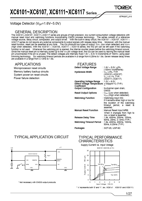
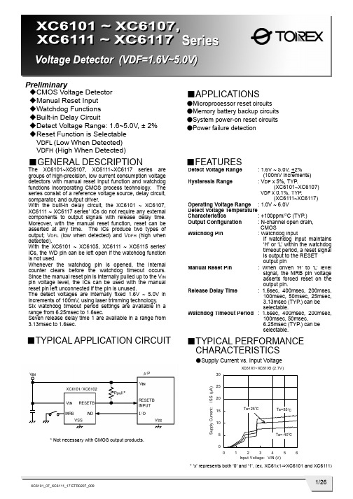
1/26XC6101_07_XC6111_17 ETR0207_009Preliminary◆CMOS Voltage Detector◆Manual Reset Input ◆Watchdog Functions ◆Built-in Delay Circuit ◆Detect Voltage Range: 1.6~5.0V, ± 2% ◆Reset Function is Selectable V DFL (Low When Detected) V DFH (High When Detected)■GENERAL DESCRIPTION The XC6101~XC6107, XC6111~XC6117 series aregroups of high-precision, low current consumption voltage detectors with manual reset input function and watchdog functions incorporating CMOS process technology. The series consist of a reference voltage source, delay circuit, comparator, and output driver.With the built-in delay circuit, the XC6101 ~ XC6107, XC6111 ~ XC6117 series’ ICs do not require any external components to output signals with release delay time. Moreover, with the manual reset function, reset can be asserted at any time. The ICs produce two types of output; V DFL (low when detected) and V DFH (high when detected).With the XC6101 ~ XC6105, XC6111 ~ XC6115 series’ ICs, the WD pin can be left open if the watchdog function is not used. Whenever the watchdog pin is opened, the internal counter clears before the watchdog timeout occurs. Since the manual reset pin is internally pulled up to the V IN pin voltage level, the ICs can be used with the manual reset pin left unconnected if the pin is unused.The detect voltages are internally fixed 1.6V ~ 5.0V in increments of 100mV, using laser trimming technology. Six watchdog timeout period settings are available in a range from 6.25msec to 1.6sec. Seven release delay time 1 are available in a range from 3.13msec to 1.6sec.■APPLICATIONS●Microprocessor reset circuits●Memory battery backup circuits ●System power-on reset circuits ●Power failure detection■TYPICAL APPLICATION CIRCUIT* Not necessary with CMOS output products.■FEATURESDetect Voltage Range: 1.6V ~ 5.0V, +2% (100mV increments)Hysteresis Range : V DF x 5%, TYP .(XC6101~XC6107)V DF x 0.1%, TYP .(XC6111~XC6117)Operating Voltage Range : 1.0V ~ 6.0V Detect Voltage Temperature Characteristics : +100ppm/O C (TYP .) Output Configuration : N-channel open drain,CMOSWatchdog Pin : Watchdog inputIf watchdog input maintains ‘H’ or ‘L’ within the watchdog timeout period, a reset signal is output to the RESET output pinManual Reset Pin : When driven ‘H’ to ‘L’levelsignal, the MRB pin voltage asserts forced reset on theoutput pin.Release Delay Time : 1.6sec, 400msec, 200msec,100msec, 50msec, 25msec, 3.13msec (TYP .) can be selectable.Watchdog Timeout Period : 1.6sec, 400msec, 200msec,100msec, 50msec,6.25msec (TYP .) can be selectable.■TYPICAL PERFORMANCE CHARACTERISTICS ●Supply Current vs. Input Voltage* ‘x’ represents both ‘0’ and ‘1’. (ex. XC61x1⇒XC6101 and XC6111)2/26XC6101~XC6107, XC6111~XC6117 SeriesPIN NUMBERXC6101, XC6102 XC6103 XC6104, XC6105XC6106, XC6107XC6111, XC6112 XC6113 XC6114, XC6115XC6116, XC6117SOT-25 USP-6C SOT-25 USP-6C SOT-25 USP-6C SOT-25USP-6CPIN NAMEFUNCTION1 4 - - 1 4 1 4 R ESETB Reset Output(V DFL : Low Level When Detected)2 5 2 5 2 5 2 5 V SSGround3 2 3 2 - -4 1 M RB ManualReset 4 1 4 1 4 1 - - WDWatchdog5 6 5 6 5 6 5 6 V IN Power Input - - 1 4 3 2 3 2 RESETReset Output (V DFH: High Level When Detected)■PIN CONFIGURATION SOT-25 (TOP VIEW)MRBV IN WD RESETBV SSMRBWD RESETV SSV IN RESETWD RESETBV SS V IN SOT-25 (TOP VIEW)RESETMRB RESETBV SS V IN SOT-25 (TOP VIEW) ■PIN ASSIGNMENT●SOT-25XC6101, XC6102 SeriesXC6111, XC6112 SeriesSOT-25 (TOP VIEW)XC6103 & XC6113 SeriesXC6104, XC6105 Series XC6114, XC6115 SeriesXC6106, XC6107 Series XC6116, XC6117 Series●USP-6CXC6101, XC6102 Series XC6111, XC6112 SeriesXC6103 & XC6113 SeriesXC6104, XC6105 Series XC6114, XC6115 SeriesXC6106, XC6107 Series XC6116, XC6117 SeriesUSP-6C (BOTTOM VIEW)USP-6C (BOTTOM VIEW)USP-6C (BOTTOM VIEW)USP-6C (BOTTOM VIEW)* The dissipation pad for the USP-6C package should be solder-plated in recommended mount pattern and metal masking so as to enhance mounting strength and heat release. If the pad needs to be connected to other pins, it should be connected to the V SS pin.3/26XC6101 ~ XC6107, XC6111~ XC6117SeriesRESET OUTPUTSERIES WATCHDOGMANUAL RESET V DFL (RESETB)V DFH (RESET)XC6101 XC6111 Available Available CMOS - XC6102XC6112AvailableAvailableN-channel open drain-XC6103 XC6113 Available Available - CMOS XC6104 XC6114 Available Not AvailableCMOS CMOS XC6105 XC6115 Available Not Available N-channel open drain CMOS XC6106 XC6116 Not Available AvailableCMOSCMOS XC6107XC6117Not AvailableAvailableN-channel open drainCMOSDESIGNATORDESCRIPTIONSYMBOLDESCRIPTION0 : V DF x 5% (TYP .) with hysteresis ① Hysteresis Range1 : V DF x 0.1% (TYP .) without hysteresis② Functions and Type of Reset Output1 ~ 7: Watchdog and manual functions, and reset output type as per Selection Guide in the above chartA : 3.13msec (TYP .)B : 25msec (TYP .) C: 50msec (TYP .) D : 100msec (TYP .) E : 200msec (TYP .) F : 400msec (TYP .) ③ Release Delay Time * H : 1.6sec (TYP .)0 : No WD timeout period forXC6106, XC6107, XC6116, XC6117 Series 1: 6.25msec (TYP .) 2 : 50msec (TYP .) 3 : 100msec (TYP .) 4 : 200msec (TYP .) 5 : 400msec (TYP .) ④ Watchdog Timeout Period6: 1.6sec (TYP .) ⑤⑥ Detect Voltage 16 ~ 50: Detect voltageex.) 4.5V: ⑤⇒4, ⑥⇒5M : SOT-25 ⑦ Package E : USP-6C R : Embossed tape, standard feed ⑧ Device OrientationL: Embossed tape, reverse feed* Please set the release delay time shorter than or equal to the watchdog timeout period. ex.) XC6101D427MR or XC6101D327MR■PRODUCT CLASSIFICATION ●Selection Guide ●Ordering Information XC61①②③④⑤⑥⑦⑧4/26XC6101~XC6107, XC6111~XC6117 Series■PACKAGING INFORMATION●SOT-25●USP-6C5/26XC6101 ~ XC6107, XC6111~ XC6117Series④ Represents production lot number0 to 9 and A to Z and inverted 0 to 9 and A to Z repeated. (G, I, J, O, Q, W expected.) * ‘X’ represents both ‘0’ and ‘1’. (ex. XC61X1⇒XC6101 and XC6111)■MARKING RULE●SOT-25①②③④SOT-25 (TOP VIEW)6/26XC6101~XC6107, XC6111~XC6117 Series① Represents product series② Represents release delay time MARK RELEASE DELAY TIME PRODUCT SERIES A 3.13msec XC61XxAxxxxx B 25msec XC61XxBxxxxx C 50msec XC61XxCxxxxx D 100msec XC61XxDxxxxx E 200msec XC61XxExxxxx F 400msec XC61XxFxxxxx H 1.6sec XC61XxHxxxxx③ Represents watchdog timeout period MARK WATCHDOG TIMEOUT PERIOD PRODUCT SERIES 0 XC61X6, XC61X7 series XC61Xxx0xxxx 1 6.25msec XC61Xxx1xxxx 2 50msec XC61Xxx2xxxx 3 100msec XC61Xxx3xxxx 4 200msec XC61Xxx4xxxx 5 400msec XC61Xxx5xxxx 6 1.6sec XC61Xxx6xxxx④⑤ Represents detect voltage MARK④ ⑤DETECT VOLTAGE (V)PRODUCT SERIES3 3 3.3 XC61Xxxx33xx 5 0 5.0XC61Xxxx50xx⑥ Represents production lot number0 to 9 and A to Z repeated. (G, I, J, O, Q, W excepted.)* No character inversion used. ** ‘X’ represents both ‘0’ and ‘1’. (ex. XC61X1⇒XC6101 and XC6111)MARK PRODUCT SERIES MARK PRODUCT SERIES 3 XC6101xxxxxx 8 XC6111xxxxxx 4 XC6102xxxxxx 9 XC6112xxxxxx 5 XC6103xxxxxx A XC6113xxxxxx 6 XC6104xxxxxx B XC6114xxxxxx 7 XC6105xxxxxx C XC6115xxxxxx 3 XC6106xxxxxx 8 XC6116xxxxxx 4 XC6107xxxxxx 9 XC6117xxxxxx■MARKING RULE (Continued)●USP-6CUSP-6C (TOP VIEW)7/26XC6101 ~ XC6107, XC6111~ XC6117Series■BLOCK DIAGRAMS●XC6101, XC6111 Series●XC6102, XC6112 Series●XC6103, XC6113 Series8/26XC6101~XC6107, XC6111~XC6117 Series■BLOCK DIAGRAMS (Continued)●XC6107, XC6117 Series●XC6106, XC6116 Series●XC6105, XC6115 Series●XC6104, XC6114 Series9/26XC6101 ~ XC6107, XC6111~ XC6117SeriesPARAMETERSYMBOL RATINGSUNITSV INV SS -0.3 ~ 7.0 VM RBV SS -0.3 ~ V IN +0.3 VInput Voltage WD V SS -0.3 ~ 7.0V Output Current I OUT 20 mACMOS Output RESETB/RESET V SS -0.3 ~ V IN +0.3Output Voltage N-ch Open Drain Output RESETB V SS -0.3 ~ 7.0VSOT-25 250Power Dissipation USP-6C Pd 100mWOperational Temperature Range Topr -40 ~ +85 OCStorage Temperature Range Tstg -40 ~ +125 OC■ABSOLUTE MAXIMUM RATINGSTa = 25O C10/26XC6101~XC6107, XC6111~XC6117 SeriesNOTE:*1: XC6101~XC6107 (with hysteresis) *2: XC6111~XC6117 (without hysteresis)*3: ‘X’ represents both ‘0’ and ‘1’. (ex. XC61X1⇒XC6101 and XC6111) *4: V DF(T): Setting detect voltage*5: If only “V DF ” is indicated, it represents both V DFL (low when detected) and V DFH (high when detected).PARAMETERSYMBOLCONDITIONSMIN.TYP .MAX. UNITS CIRCUITDetect Voltage V DFL V DFHV DF(T)× 0.98V DF(T) V DF(T)× 1.02 V 1 Hysteresis Range XC6101~XC6107 (*1) V HYS V DF × 0.02V DF × 0.05 V DF× 0.08 V 1Hysteresis Range XC6111~XC6117 (*2) V HYS 0 V DF × 0.001 V DFx 0.01V 1V IN =V DF(T)×0.9V - 5 11 V IN =V DF(T)×1.1V- 10 16 XC61X1/XC61X2/XC61X3XC61X4/XC61X5 (*3)(The MRB & the WD Pin: No connection) V IN =6.0V - 1218 V IN =V DF(T)×0.9V - 4 10 V IN =V DF(T)×1.1V - 8 14 Supply Current I SS XC61X6/XC61X7 (*3)(The MRB Pin: No connection)V IN = 6.0V - 1016 µA 2Operating Voltage V IN 1.0 - 6.0 V 1VIN = 1.0V 0.15 0.5 -V IN =2.0V (V DFL(T)> 2.0V) 2.0 2.5 - V IN =3.0V (V DFL(T) >3.0V) 3.0 3.5 -N-ch.V DS = 0.5V V IN =4.0V (V DFL(T) >4.0V) 3.5 4.0 - 3 V DFL Output Current (RESETB) I RBOUTCMOS,P-chV DS = 0.5V V IN = 6.0V - - 1.1 -0.8 mA 4 N-chV DS = 0.5VV IN =6.0V 4.4 4.9 - 3V IN =1.0V - - 0.08 - 0.02 V IN =2.0V (V DFH(T)> 2.0V)- - 0.50 - 0.30 V IN =3.0V (V DFH(T)>3.0V)- - 0.75 - 0.55V DFHOutput Current (RESET) I ROUT P-ch. V DS = 0.5V V IN =4.0V (V DFH(T)>4.0V)- - 0.95 - 0.75 mA 4Temperature Characteristics △V DF / △Topr ・V DF -40OC < Topr < 85 O C - +100 - ppm / O C12 3.13 5 13 25 3825 50 75 60 100 140 120 200 280 240 400 560Release Delay Time(V DF <1.8V)T DR Time until V IN is increased from1.0V to2.0Vand attains to the release time level,and the Reset output pin inverts.960 1600 2240 ms 5 2 3.13 5 13 25 38 25 50 7560 100 140 120 200 280 240 400 560 Release Delay Time(V DF >1.9V)T DRTime until V IN is increased from1.0V to (V DF x1.1V) and attains to the releasetime level,and the Reset output pin inverts. 960 1600 2240ms 5 Detect Delay Time T DFTime until V IN is decreased from 6.0V to 1.0V and attains to the detect voltage level, and the Reset output pin detectswhile the WD pin left opened.- 3 30 µs 5V DFL /V DFH CMOS Output Leak CurrentI LEAK V IN =6.0V, RESETB=6.0V (V DFL ) V IN =6.0V, RESET=0V (V DFH )- 0.01 - µA 3V DFL N-ch Open DrainOutput Leak CurrentI LEAKV IN =6.0V, RESETB=6.0V-0.010.10µA 3■ELECTRICAL CHARACTERISTICS●XC6101~XC6107, XC6111~XC6117 SeriesTa = 25O CSeriesPARAMETERSYMBOL CONDITIONS MIN.TYP . MAX. UNITS CIRCUIT3.13 6.25 9.38 25 50 7560 100 140 120 200 280240 400 560 Watchdog Timeout Period (V DF <1.8V)T WDTime until V IN increases form1.0V to2.0V andthe Reset output pin is released to go into the detection state. (WD=V SS )960 1600 2240 ms 6 3.13 6.25 9.38 25 50 75 60 100 140 120 200 280240 400 560 Watchdog Timeout Period (V DF >1.9V)T WDTime until V IN increases form1.0V to (V DF x1.1V)and the Reset output pin is released to go into the detection state. (WD=V SS )960 1600 2240 ms 6 WatchdogMinimum Pulse Width T WDIN V IN =6.0V,Apply pulse from 6.0V to 0Vto the WD pin. 300 - - ns 7 Watchdog High Level VoltageV WDH V IN =V DF x 1.1V ~ 6.0V V IN x 0.7- 6 V 7 Watchdog Low Level Voltage V WDL V IN =V DF x 1.1V ~ 6.0V0 - V IN x 0.3 V 7 V IN =6.0V, V WD =6.0V (Avg. when peak )- 12 19Watchdog Input Current I WD V IN =6.0V, V WD =0V (Avg. when peak) - 19 -12 -µA 8 Watchdog Input ResistanceR WDV IN =6.0V, V WD =0V, R WD =V IN / |I WD |315500880k Ω8PARAMETERSYMBOL CONDITIONS MIN.TYP . MAX.UNITS CIRCUITMRBHigh Level VoltageV MRH V IN =V DF x1.1V ~ 6.0V 1.4 - V IN 9MRBLow Level VoltageV MRL V IN =V DF x1.1V ~ 6.0V-0.35 V9MRBPull-up Resistance R MR V IN =6.0V, MRB=0V, R MR =V IN / |I MRB | 1.6 2.4 3.0 M Ω 10 MRB Minimum Pulse Width (*3) XC6101~XC6105 XC6111~XC6115 T MRINV IN =6.0V,Apply pulse from 6.0V to 0V tothe MRB pin 2.8 - -MRB Minimum Pulse Width (*4) XC6106, XC6107 XC6116, XC6117T MRIN V IN =6.0V,Apply pulse from 6.0V to 0V tothe MRB pin1.2 - -µs11●XC6101 ~ XC6103, XC6106 ~ XC6107, XC6111 ~ XC6113, XC6116 ~ XC6117 Series NOTE:*1: V DF(T): Setting detect voltage *2: If only “V DF ” is indicated, it represents both V DFL (low when detected) and V DFH (high when detected). *3: Watchdog function is available. *4: Watchdog function is not available.Ta = 25O CTa = 25O C ■ELECTRICAL CHARACTERISTICS (Continued)●XC6101~XC6105, XC6111~XC6115 Series■OPERATIONAL EXPLANATIONThe XC6101~XC6107, XC6111~XC6117 series compare, using the error amplifier, the voltage of the internal voltage reference source with the voltage divided by R1, R2 and R3 connected to the V IN pin. The resulting output signal from the error amplifier activates the watchdog logic, manual reset logic, delay circuit and the output driver. When the V IN pin voltage gradually falls and finally reaches the detect voltage, the RESETB pin output goes from high to low in the case of the V DFL type ICs, and the RESET pin output goes from low to high in the case of the V DFH type ICs.<RESETB / RESET Pin Output Signal>* V DFL (RESETB) type - output signal: Low when detected.The RESETB pin output goes from high to low whenever the V IN pin voltage falls below the detect voltage, or whenever the MRB pin is driven from high to low. The RESETB pin remains low for the release delay time (T DR) after the V IN pin voltage reaches the release voltage. If neither rising nor falling signals are applied to the WD pin within the watchdog timeout period, the RESETB pin output remains low for the release delay time (T DR), and thereafter the RESET pin outputs high level signal. * V DFH (RESET) type – output signal: High when detected.The RESET pin output goes from low to high whenever the V IN pin voltage falls below the detect voltage, or whenever the MRB pin is driven from high to low. The RESET pin remains high for the release delay time (T DR) after the V IN pin voltage reaches the release voltage. If neither rising nor falling signals are applied to the WD pin within the watchdog timeout period, the V OUT pin output remains high for the release delay time (T DR), and thereafter the RESET pin outputs low level signal.<Hysteresis>When the internal comparator output is high, the NMOS transistor connected in parallel to R3 is turned ON, activating the hysteresis circuit. The difference between the release and detect voltages represents the hysteresis range, as shown by the following calculations:V DF (detect voltage) = (R1+R2+R3) x Vref(R2+R3)V DR (release voltage) = (R1+R2) x Vref(R2)V HYS (hysteresis range)=V DR-V DF (V)V DR > V DF* Detect voltage (V DF) includes conditions of both V DFL (low when detected) and V DFH (high when detected).* Please refer to the block diagrams for R1, R2, R3 and Vref.Hysteresis range is selectable from V DF x 0.05V (XC6101~XC6107) or V DF x 0.001V (XC6111~XC6117).<Watchdog (WD) Pin>The XC6101~XC6107, XC6111~XC6117 series use a watchdog timer to detect malfunction or “runaway” of the microprocessor. If neither rising nor falling signals are applied from the microprocessor within the watchdog timeout period, the RESETB/RESET pin output maintains the detection state for the release delay time (T DR), and thereafter the RESET/RESETB pin output returns to the release state (Please refer to the FUNCTION CHART). The timer in the watchdog is then restarted. Six watchdog timeout period settings are available in 1.6sec, 400msec, 200msec, 100msec, 50msec, 6.25msec.<MRB Pin>Using the MRB pin input, the RESET/RESETB pin signal can be forced to the detection state. When the MRB pin is driven from high to low, the RESETB pin output goes from high to low in the case of the V DFL type ICs, and the RESET pin output goes from low to high in the case of the V DFH type. Even after the MRB pin is driven back high, the RESET/RESETB pin output maintains the detection state for the release delay time (T DR). Since the MRB pin is internally pulled up to the V IN pin voltage level, leave the MRB pin open if unused (Please refer to the FUNCTION CHART). A diode, which is an input protection element, is connected between the MRB pin and V IN pin. Therefore, if the MRB pin is applied voltage that exceeds V IN, the current will flow to V IN through the diode. Please use this IC within the stated maximum ratings (V SS -0.3 ~ V IN+0.3) on the MRB pin.<Release Delay Time>Release delay time (T DR) is the time that elapses from when the V IN pin reaches the release voltage, or when the watchdog timeout period expires with no rising signal applied to the WD pin, until the RESET/RESETB pin output is released from the detection state. Seven release delay time (T DR) watchdog timeout period settings are available in 1.6sec, 400msec, 200msec, 100msec, 50msec, 25msec, 3.13msec.<Detect Delay Time>Detect Delay Time (T DF) is the time that elapses from when the V IN pin voltage falls to the detect voltage until the RESET/ RESETB pin output goes into the detection state.Series■TIMING CHARTS●CMOS Output●T DF (CMOS Output)VINVDFL LevelGNDVIN Level VDFL Level GNDVIN x 0.1V■NOTES ON USE1. Please use this IC within the stated maximum ratings. Operation beyond these limits may cause degrading or permanent damage to the device.2. When a resistor is connected between the V IN pin and the input, the V IN voltage drops while the IC is operating and a malfunction may occur as a result of the IC’s through current. For the CMOS output products, the V IN voltage drops while the IC is operating and malfunction may occur as a result of the IC’s output current. Please be careful with using the XC6111~XC6117 series (without hysteresis).3. In order to stabilize the IC’s operations, please ensure that the V IN pin’s input frequency’s rise and fall times are more than 1 µ sec/V.4. Noise at the power supply may cause a malfunction of the watchdog operation or the circuit. In such case, please strength the line between V IN and the GND pin and connect about 0.22µF of a capacitor between the V IN pin and the GND pin.5. Protecting against a malfunction while the watchdog time out period, an ignoring time (no reaction time) occurs to the rise and fall times. Referring to the figure below, the ignoring time (no reaction time) lasts for 900µsec at maximum.GNDGNDGNDVIN Pin Wave FormWD Pin Wave FormRESETB Pin Wave Form (VDFL)SeriesPIN NAMELOGIC CONDITIONSH V IN >V DF +V HYS V IN L V IN <V DF H MRB>1.40V MRBL MRB<0.35V H When keeping W D >V WDH more than T WD L When keeping W D <V WDL more than T WD L → H V WDL → V WDH , T WDIN >300nsec WDH → L V WDH →V WDH , T WDIN >300nsecV IN MRB WD RESETB (*2) H HH LRepeat detect and release (H →L →H)H OpenH L → HH H or Open H → L H HLL *1 LV IN MRB WD RESETB (*3) H HH LRepeat detect and release (L →H →L)H OpenH L → HH H or Open H → L L HLL *1 HV IN WD RESETB (*2) RESET (*3) H HH L Repeat detect and release (H →L →H)Repeat detect and release (L →H →L)H OpenH L → HH H → L H L HL*1 L HV IN MRB RESETB (*2)RESET (*3)H H or Open H LH LL L H■PIN LOGIC CONDITIONSNOTE:*1: If only “V DF ” is indicated, it represents both V DFL (low when detected) and V DFH (high when detected).*2: For the details of each parameter, please see the electrical characteristics. V DF : Detect VoltageV HYS : Hysteresis RangeV WDH : WD High Level Voltage V WDL: WD Low Level Voltage T WDIN : WD Pulse Width T WD : WD Timeout Period■FUNCTION CHART●XC6103/XC61113 Series●XC6104/XC61114, XC6105/XC6115 Series●XC6106/XC61116, XC6107/XC6117 Series●XC6101/XC61111, XC6102/6112 Series*1: Including all logic of WD (WD=H, L, L →H, H →L, OPEN). *2: When the RESETB is High, the circuit is in the release state. When the RESETB is Low, the circuit is in the detection state. *3: When the RESET is High, the circuit is in the release state. When the RESET is Low, the circuit is in the detection state.■TEST CIRCUITSCircuit 1Circuit 2Circuit 3Circuit 4Series ■TEST CIRCUITS (Continued)Circuit 5Circuit 6Circuit 7■TEST CIRCUITS (Continued)Circuit 8Circuit 9Circuit 10Circuit 11Series■TYPICAL PERFORMANCE CHARACTERISTICS(1.1) Supply Current vs. Input Voltage(1.2) Supply Current vs. Input Voltage■TYPICAL PERFORMANCE CHARACTERISTICS (Continued)(2) Detect, Release Voltage vs. Ambient Temperature(1.2) Supply Current vs. Input Voltage (Continued)Series■TYPICAL PERFORMANCE CHARACTERISTICS (Continued) (3-1) Output Voltage vs. Input Voltage (V DFL ) (3.1) Detect, Release Voltage vs. Input Voltage (V DFL )(3.2) Detect, Release Voltage vs. Input Voltage (V DFH )■TYPICAL PERFORMANCE CHARACTERISTICS (Continued)(4) N-ch Driver Output Current vs. V DSSeries(6) P-ch Driver Output Current vs. Input Voltage 1■TYPICAL PERFORMANCE CHARACTERISTICS (Continued)(8) Release Delay Time vs. Ambient Temperature(7) P-ch Driver Output Current vs. Input Voltage 2■TYPICAL PERFORMANCE CHARACTERISTICS (Continued) (10) Release Delay Time vs. Input Voltage(11) Watchdog Timeout Period vs. Input VoltageSeries■TYPICAL PERFORMANCE CHARACTERISTICS (Continued)(14) MRB Low Level Voltage vs. Ambient Temperature(15) MRB High Level Voltage vs. Ambient Temperature* ‘X’ represents both ‘0’ and ‘1’. (ex. XC61X1⇒XC6101 and XC6111)。
XC6103D629资料

1/26XC6101_07_XC6111_17 ETR0207_009Preliminary◆CMOS Voltage Detector◆Manual Reset Input ◆Watchdog Functions ◆Built-in Delay Circuit ◆Detect Voltage Range: 1.6~5.0V, ± 2% ◆Reset Function is Selectable V DFL (Low When Detected) V DFH (High When Detected)■GENERAL DESCRIPTION The XC6101~XC6107, XC6111~XC6117 series aregroups of high-precision, low current consumption voltage detectors with manual reset input function and watchdog functions incorporating CMOS process technology. The series consist of a reference voltage source, delay circuit, comparator, and output driver.With the built-in delay circuit, the XC6101 ~ XC6107, XC6111 ~ XC6117 series’ ICs do not require any external components to output signals with release delay time. Moreover, with the manual reset function, reset can be asserted at any time. The ICs produce two types of output; V DFL (low when detected) and V DFH (high when detected).With the XC6101 ~ XC6105, XC6111 ~ XC6115 series’ ICs, the WD pin can be left open if the watchdog function is not used. Whenever the watchdog pin is opened, the internal counter clears before the watchdog timeout occurs. Since the manual reset pin is internally pulled up to the V IN pin voltage level, the ICs can be used with the manual reset pin left unconnected if the pin is unused.The detect voltages are internally fixed 1.6V ~ 5.0V in increments of 100mV, using laser trimming technology. Six watchdog timeout period settings are available in a range from 6.25msec to 1.6sec. Seven release delay time 1 are available in a range from 3.13msec to 1.6sec.■APPLICATIONS●Microprocessor reset circuits●Memory battery backup circuits ●System power-on reset circuits ●Power failure detection■TYPICAL APPLICATION CIRCUIT* Not necessary with CMOS output products.■FEATURESDetect Voltage Range: 1.6V ~ 5.0V, +2% (100mV increments)Hysteresis Range : V DF x 5%, TYP .(XC6101~XC6107)V DF x 0.1%, TYP .(XC6111~XC6117)Operating Voltage Range : 1.0V ~ 6.0V Detect Voltage Temperature Characteristics : +100ppm/O C (TYP .) Output Configuration : N-channel open drain,CMOSWatchdog Pin : Watchdog inputIf watchdog input maintains ‘H’ or ‘L’ within the watchdog timeout period, a reset signal is output to the RESET output pinManual Reset Pin : When driven ‘H’ to ‘L’levelsignal, the MRB pin voltage asserts forced reset on theoutput pin.Release Delay Time : 1.6sec, 400msec, 200msec,100msec, 50msec, 25msec, 3.13msec (TYP .) can be selectable.Watchdog Timeout Period : 1.6sec, 400msec, 200msec,100msec, 50msec,6.25msec (TYP .) can be selectable.■TYPICAL PERFORMANCE CHARACTERISTICS ●Supply Current vs. Input Voltage* ‘x’ represents both ‘0’ and ‘1’. (ex. XC61x1⇒XC6101 and XC6111)2/26XC6101~XC6107, XC6111~XC6117 SeriesPIN NUMBERXC6101, XC6102 XC6103 XC6104, XC6105XC6106, XC6107XC6111, XC6112 XC6113 XC6114, XC6115XC6116, XC6117SOT-25 USP-6C SOT-25 USP-6C SOT-25 USP-6C SOT-25USP-6CPIN NAMEFUNCTION1 4 - - 1 4 1 4 R ESETB Reset Output(V DFL : Low Level When Detected)2 5 2 5 2 5 2 5 V SSGround3 2 3 2 - -4 1 M RB ManualReset 4 1 4 1 4 1 - - WDWatchdog5 6 5 6 5 6 5 6 V IN Power Input - - 1 4 3 2 3 2 RESETReset Output (V DFH: High Level When Detected)■PIN CONFIGURATION SOT-25 (TOP VIEW)MRBV IN WD RESETBV SSMRBWD RESETV SSV IN RESETWD RESETBV SS V IN SOT-25 (TOP VIEW)RESETMRB RESETBV SS V IN SOT-25 (TOP VIEW) ■PIN ASSIGNMENT●SOT-25XC6101, XC6102 SeriesXC6111, XC6112 SeriesSOT-25 (TOP VIEW)XC6103 & XC6113 SeriesXC6104, XC6105 Series XC6114, XC6115 SeriesXC6106, XC6107 Series XC6116, XC6117 Series●USP-6CXC6101, XC6102 Series XC6111, XC6112 SeriesXC6103 & XC6113 SeriesXC6104, XC6105 Series XC6114, XC6115 SeriesXC6106, XC6107 Series XC6116, XC6117 SeriesUSP-6C (BOTTOM VIEW)USP-6C (BOTTOM VIEW)USP-6C (BOTTOM VIEW)USP-6C (BOTTOM VIEW)* The dissipation pad for the USP-6C package should be solder-plated in recommended mount pattern and metal masking so as to enhance mounting strength and heat release. If the pad needs to be connected to other pins, it should be connected to the V SS pin.3/26XC6101 ~ XC6107, XC6111~ XC6117SeriesRESET OUTPUTSERIES WATCHDOGMANUAL RESET V DFL (RESETB)V DFH (RESET)XC6101 XC6111 Available Available CMOS - XC6102XC6112AvailableAvailableN-channel open drain-XC6103 XC6113 Available Available - CMOS XC6104 XC6114 Available Not AvailableCMOS CMOS XC6105 XC6115 Available Not Available N-channel open drain CMOS XC6106 XC6116 Not Available AvailableCMOSCMOS XC6107XC6117Not AvailableAvailableN-channel open drainCMOSDESIGNATORDESCRIPTIONSYMBOLDESCRIPTION0 : V DF x 5% (TYP .) with hysteresis ① Hysteresis Range1 : V DF x 0.1% (TYP .) without hysteresis② Functions and Type of Reset Output1 ~ 7: Watchdog and manual functions, and reset output type as per Selection Guide in the above chartA : 3.13msec (TYP .)B : 25msec (TYP .) C: 50msec (TYP .) D : 100msec (TYP .) E : 200msec (TYP .) F : 400msec (TYP .) ③ Release Delay Time * H : 1.6sec (TYP .)0 : No WD timeout period forXC6106, XC6107, XC6116, XC6117 Series 1: 6.25msec (TYP .) 2 : 50msec (TYP .) 3 : 100msec (TYP .) 4 : 200msec (TYP .) 5 : 400msec (TYP .) ④ Watchdog Timeout Period6: 1.6sec (TYP .) ⑤⑥ Detect Voltage 16 ~ 50: Detect voltageex.) 4.5V: ⑤⇒4, ⑥⇒5M : SOT-25 ⑦ Package E : USP-6C R : Embossed tape, standard feed ⑧ Device OrientationL: Embossed tape, reverse feed* Please set the release delay time shorter than or equal to the watchdog timeout period. ex.) XC6101D427MR or XC6101D327MR■PRODUCT CLASSIFICATION ●Selection Guide ●Ordering Information XC61①②③④⑤⑥⑦⑧4/26XC6101~XC6107, XC6111~XC6117 Series■PACKAGING INFORMATION●SOT-25●USP-6C5/26XC6101 ~ XC6107, XC6111~ XC6117Series④ Represents production lot number0 to 9 and A to Z and inverted 0 to 9 and A to Z repeated. (G, I, J, O, Q, W expected.) * ‘X’ represents both ‘0’ and ‘1’. (ex. XC61X1⇒XC6101 and XC6111)■MARKING RULE●SOT-25①②③④SOT-25 (TOP VIEW)6/26XC6101~XC6107, XC6111~XC6117 Series① Represents product series② Represents release delay time MARK RELEASE DELAY TIME PRODUCT SERIES A 3.13msec XC61XxAxxxxx B 25msec XC61XxBxxxxx C 50msec XC61XxCxxxxx D 100msec XC61XxDxxxxx E 200msec XC61XxExxxxx F 400msec XC61XxFxxxxx H 1.6sec XC61XxHxxxxx③ Represents watchdog timeout period MARK WATCHDOG TIMEOUT PERIOD PRODUCT SERIES 0 XC61X6, XC61X7 series XC61Xxx0xxxx 1 6.25msec XC61Xxx1xxxx 2 50msec XC61Xxx2xxxx 3 100msec XC61Xxx3xxxx 4 200msec XC61Xxx4xxxx 5 400msec XC61Xxx5xxxx 6 1.6sec XC61Xxx6xxxx④⑤ Represents detect voltage MARK④ ⑤DETECT VOLTAGE (V)PRODUCT SERIES3 3 3.3 XC61Xxxx33xx 5 0 5.0XC61Xxxx50xx⑥ Represents production lot number0 to 9 and A to Z repeated. (G, I, J, O, Q, W excepted.)* No character inversion used. ** ‘X’ represents both ‘0’ and ‘1’. (ex. XC61X1⇒XC6101 and XC6111)MARK PRODUCT SERIES MARK PRODUCT SERIES 3 XC6101xxxxxx 8 XC6111xxxxxx 4 XC6102xxxxxx 9 XC6112xxxxxx 5 XC6103xxxxxx A XC6113xxxxxx 6 XC6104xxxxxx B XC6114xxxxxx 7 XC6105xxxxxx C XC6115xxxxxx 3 XC6106xxxxxx 8 XC6116xxxxxx 4 XC6107xxxxxx 9 XC6117xxxxxx■MARKING RULE (Continued)●USP-6CUSP-6C (TOP VIEW)7/26XC6101 ~ XC6107, XC6111~ XC6117Series■BLOCK DIAGRAMS●XC6101, XC6111 Series●XC6102, XC6112 Series●XC6103, XC6113 Series8/26XC6101~XC6107, XC6111~XC6117 Series■BLOCK DIAGRAMS (Continued)●XC6107, XC6117 Series●XC6106, XC6116 Series●XC6105, XC6115 Series●XC6104, XC6114 Series9/26XC6101 ~ XC6107, XC6111~ XC6117SeriesPARAMETERSYMBOL RATINGSUNITSV INV SS -0.3 ~ 7.0 VM RBV SS -0.3 ~ V IN +0.3 VInput Voltage WD V SS -0.3 ~ 7.0V Output Current I OUT 20 mACMOS Output RESETB/RESET V SS -0.3 ~ V IN +0.3Output Voltage N-ch Open Drain Output RESETB V SS -0.3 ~ 7.0VSOT-25 250Power Dissipation USP-6C Pd 100mWOperational Temperature Range Topr -40 ~ +85 OCStorage Temperature Range Tstg -40 ~ +125 OC■ABSOLUTE MAXIMUM RATINGSTa = 25O C10/26XC6101~XC6107, XC6111~XC6117 SeriesNOTE:*1: XC6101~XC6107 (with hysteresis) *2: XC6111~XC6117 (without hysteresis)*3: ‘X’ represents both ‘0’ and ‘1’. (ex. XC61X1⇒XC6101 and XC6111) *4: V DF(T): Setting detect voltage*5: If only “V DF ” is indicated, it represents both V DFL (low when detected) and V DFH (high when detected).PARAMETERSYMBOLCONDITIONSMIN.TYP .MAX. UNITS CIRCUITDetect Voltage V DFL V DFHV DF(T)× 0.98V DF(T) V DF(T)× 1.02 V 1 Hysteresis Range XC6101~XC6107 (*1) V HYS V DF × 0.02V DF × 0.05 V DF× 0.08 V 1Hysteresis Range XC6111~XC6117 (*2) V HYS 0 V DF × 0.001 V DFx 0.01V 1V IN =V DF(T)×0.9V - 5 11 V IN =V DF(T)×1.1V- 10 16 XC61X1/XC61X2/XC61X3XC61X4/XC61X5 (*3)(The MRB & the WD Pin: No connection) V IN =6.0V - 1218 V IN =V DF(T)×0.9V - 4 10 V IN =V DF(T)×1.1V - 8 14 Supply Current I SS XC61X6/XC61X7 (*3)(The MRB Pin: No connection)V IN = 6.0V - 1016 µA 2Operating Voltage V IN 1.0 - 6.0 V 1VIN = 1.0V 0.15 0.5 -V IN =2.0V (V DFL(T)> 2.0V) 2.0 2.5 - V IN =3.0V (V DFL(T) >3.0V) 3.0 3.5 -N-ch.V DS = 0.5V V IN =4.0V (V DFL(T) >4.0V) 3.5 4.0 - 3 V DFL Output Current (RESETB) I RBOUTCMOS,P-chV DS = 0.5V V IN = 6.0V - - 1.1 -0.8 mA 4 N-chV DS = 0.5VV IN =6.0V 4.4 4.9 - 3V IN =1.0V - - 0.08 - 0.02 V IN =2.0V (V DFH(T)> 2.0V)- - 0.50 - 0.30 V IN =3.0V (V DFH(T)>3.0V)- - 0.75 - 0.55V DFHOutput Current (RESET) I ROUT P-ch. V DS = 0.5V V IN =4.0V (V DFH(T)>4.0V)- - 0.95 - 0.75 mA 4Temperature Characteristics △V DF / △Topr ・V DF -40OC < Topr < 85 O C - +100 - ppm / O C12 3.13 5 13 25 3825 50 75 60 100 140 120 200 280 240 400 560Release Delay Time(V DF <1.8V)T DR Time until V IN is increased from1.0V to2.0Vand attains to the release time level,and the Reset output pin inverts.960 1600 2240 ms 5 2 3.13 5 13 25 38 25 50 7560 100 140 120 200 280 240 400 560 Release Delay Time(V DF >1.9V)T DRTime until V IN is increased from1.0V to (V DF x1.1V) and attains to the releasetime level,and the Reset output pin inverts. 960 1600 2240ms 5 Detect Delay Time T DFTime until V IN is decreased from 6.0V to 1.0V and attains to the detect voltage level, and the Reset output pin detectswhile the WD pin left opened.- 3 30 µs 5V DFL /V DFH CMOS Output Leak CurrentI LEAK V IN =6.0V, RESETB=6.0V (V DFL ) V IN =6.0V, RESET=0V (V DFH )- 0.01 - µA 3V DFL N-ch Open DrainOutput Leak CurrentI LEAKV IN =6.0V, RESETB=6.0V-0.010.10µA 3■ELECTRICAL CHARACTERISTICS●XC6101~XC6107, XC6111~XC6117 SeriesTa = 25O CSeriesPARAMETERSYMBOL CONDITIONS MIN.TYP . MAX. UNITS CIRCUIT3.13 6.25 9.38 25 50 7560 100 140 120 200 280240 400 560 Watchdog Timeout Period (V DF <1.8V)T WDTime until V IN increases form1.0V to2.0V andthe Reset output pin is released to go into the detection state. (WD=V SS )960 1600 2240 ms 6 3.13 6.25 9.38 25 50 75 60 100 140 120 200 280240 400 560 Watchdog Timeout Period (V DF >1.9V)T WDTime until V IN increases form1.0V to (V DF x1.1V)and the Reset output pin is released to go into the detection state. (WD=V SS )960 1600 2240 ms 6 WatchdogMinimum Pulse Width T WDIN V IN =6.0V,Apply pulse from 6.0V to 0Vto the WD pin. 300 - - ns 7 Watchdog High Level VoltageV WDH V IN =V DF x 1.1V ~ 6.0V V IN x 0.7- 6 V 7 Watchdog Low Level Voltage V WDL V IN =V DF x 1.1V ~ 6.0V0 - V IN x 0.3 V 7 V IN =6.0V, V WD =6.0V (Avg. when peak )- 12 19Watchdog Input Current I WD V IN =6.0V, V WD =0V (Avg. when peak) - 19 -12 -µA 8 Watchdog Input ResistanceR WDV IN =6.0V, V WD =0V, R WD =V IN / |I WD |315500880k Ω8PARAMETERSYMBOL CONDITIONS MIN.TYP . MAX.UNITS CIRCUITMRBHigh Level VoltageV MRH V IN =V DF x1.1V ~ 6.0V 1.4 - V IN 9MRBLow Level VoltageV MRL V IN =V DF x1.1V ~ 6.0V-0.35 V9MRBPull-up Resistance R MR V IN =6.0V, MRB=0V, R MR =V IN / |I MRB | 1.6 2.4 3.0 M Ω 10 MRB Minimum Pulse Width (*3) XC6101~XC6105 XC6111~XC6115 T MRINV IN =6.0V,Apply pulse from 6.0V to 0V tothe MRB pin 2.8 - -MRB Minimum Pulse Width (*4) XC6106, XC6107 XC6116, XC6117T MRIN V IN =6.0V,Apply pulse from 6.0V to 0V tothe MRB pin1.2 - -µs11●XC6101 ~ XC6103, XC6106 ~ XC6107, XC6111 ~ XC6113, XC6116 ~ XC6117 Series NOTE:*1: V DF(T): Setting detect voltage *2: If only “V DF ” is indicated, it represents both V DFL (low when detected) and V DFH (high when detected). *3: Watchdog function is available. *4: Watchdog function is not available.Ta = 25O CTa = 25O C ■ELECTRICAL CHARACTERISTICS (Continued)●XC6101~XC6105, XC6111~XC6115 Series■OPERATIONAL EXPLANATIONThe XC6101~XC6107, XC6111~XC6117 series compare, using the error amplifier, the voltage of the internal voltage reference source with the voltage divided by R1, R2 and R3 connected to the V IN pin. The resulting output signal from the error amplifier activates the watchdog logic, manual reset logic, delay circuit and the output driver. When the V IN pin voltage gradually falls and finally reaches the detect voltage, the RESETB pin output goes from high to low in the case of the V DFL type ICs, and the RESET pin output goes from low to high in the case of the V DFH type ICs.<RESETB / RESET Pin Output Signal>* V DFL (RESETB) type - output signal: Low when detected.The RESETB pin output goes from high to low whenever the V IN pin voltage falls below the detect voltage, or whenever the MRB pin is driven from high to low. The RESETB pin remains low for the release delay time (T DR) after the V IN pin voltage reaches the release voltage. If neither rising nor falling signals are applied to the WD pin within the watchdog timeout period, the RESETB pin output remains low for the release delay time (T DR), and thereafter the RESET pin outputs high level signal. * V DFH (RESET) type – output signal: High when detected.The RESET pin output goes from low to high whenever the V IN pin voltage falls below the detect voltage, or whenever the MRB pin is driven from high to low. The RESET pin remains high for the release delay time (T DR) after the V IN pin voltage reaches the release voltage. If neither rising nor falling signals are applied to the WD pin within the watchdog timeout period, the V OUT pin output remains high for the release delay time (T DR), and thereafter the RESET pin outputs low level signal.<Hysteresis>When the internal comparator output is high, the NMOS transistor connected in parallel to R3 is turned ON, activating the hysteresis circuit. The difference between the release and detect voltages represents the hysteresis range, as shown by the following calculations:V DF (detect voltage) = (R1+R2+R3) x Vref(R2+R3)V DR (release voltage) = (R1+R2) x Vref(R2)V HYS (hysteresis range)=V DR-V DF (V)V DR > V DF* Detect voltage (V DF) includes conditions of both V DFL (low when detected) and V DFH (high when detected).* Please refer to the block diagrams for R1, R2, R3 and Vref.Hysteresis range is selectable from V DF x 0.05V (XC6101~XC6107) or V DF x 0.001V (XC6111~XC6117).<Watchdog (WD) Pin>The XC6101~XC6107, XC6111~XC6117 series use a watchdog timer to detect malfunction or “runaway” of the microprocessor. If neither rising nor falling signals are applied from the microprocessor within the watchdog timeout period, the RESETB/RESET pin output maintains the detection state for the release delay time (T DR), and thereafter the RESET/RESETB pin output returns to the release state (Please refer to the FUNCTION CHART). The timer in the watchdog is then restarted. Six watchdog timeout period settings are available in 1.6sec, 400msec, 200msec, 100msec, 50msec, 6.25msec.<MRB Pin>Using the MRB pin input, the RESET/RESETB pin signal can be forced to the detection state. When the MRB pin is driven from high to low, the RESETB pin output goes from high to low in the case of the V DFL type ICs, and the RESET pin output goes from low to high in the case of the V DFH type. Even after the MRB pin is driven back high, the RESET/RESETB pin output maintains the detection state for the release delay time (T DR). Since the MRB pin is internally pulled up to the V IN pin voltage level, leave the MRB pin open if unused (Please refer to the FUNCTION CHART). A diode, which is an input protection element, is connected between the MRB pin and V IN pin. Therefore, if the MRB pin is applied voltage that exceeds V IN, the current will flow to V IN through the diode. Please use this IC within the stated maximum ratings (V SS -0.3 ~ V IN+0.3) on the MRB pin.<Release Delay Time>Release delay time (T DR) is the time that elapses from when the V IN pin reaches the release voltage, or when the watchdog timeout period expires with no rising signal applied to the WD pin, until the RESET/RESETB pin output is released from the detection state. Seven release delay time (T DR) watchdog timeout period settings are available in 1.6sec, 400msec, 200msec, 100msec, 50msec, 25msec, 3.13msec.<Detect Delay Time>Detect Delay Time (T DF) is the time that elapses from when the V IN pin voltage falls to the detect voltage until the RESET/ RESETB pin output goes into the detection state.Series■TIMING CHARTS●CMOS Output●T DF (CMOS Output)VINVDFL LevelGNDVIN Level VDFL Level GNDVIN x 0.1V■NOTES ON USE1. Please use this IC within the stated maximum ratings. Operation beyond these limits may cause degrading or permanent damage to the device.2. When a resistor is connected between the V IN pin and the input, the V IN voltage drops while the IC is operating and a malfunction may occur as a result of the IC’s through current. For the CMOS output products, the V IN voltage drops while the IC is operating and malfunction may occur as a result of the IC’s output current. Please be careful with using the XC6111~XC6117 series (without hysteresis).3. In order to stabilize the IC’s operations, please ensure that the V IN pin’s input frequency’s rise and fall times are more than 1 µ sec/V.4. Noise at the power supply may cause a malfunction of the watchdog operation or the circuit. In such case, please strength the line between V IN and the GND pin and connect about 0.22µF of a capacitor between the V IN pin and the GND pin.5. Protecting against a malfunction while the watchdog time out period, an ignoring time (no reaction time) occurs to the rise and fall times. Referring to the figure below, the ignoring time (no reaction time) lasts for 900µsec at maximum.GNDGNDGNDVIN Pin Wave FormWD Pin Wave FormRESETB Pin Wave Form (VDFL)SeriesPIN NAMELOGIC CONDITIONSH V IN >V DF +V HYS V IN L V IN <V DF H MRB>1.40V MRBL MRB<0.35V H When keeping W D >V WDH more than T WD L When keeping W D <V WDL more than T WD L → H V WDL → V WDH , T WDIN >300nsec WDH → L V WDH →V WDH , T WDIN >300nsecV IN MRB WD RESETB (*2) H HH LRepeat detect and release (H →L →H)H OpenH L → HH H or Open H → L H HLL *1 LV IN MRB WD RESETB (*3) H HH LRepeat detect and release (L →H →L)H OpenH L → HH H or Open H → L L HLL *1 HV IN WD RESETB (*2) RESET (*3) H HH L Repeat detect and release (H →L →H)Repeat detect and release (L →H →L)H OpenH L → HH H → L H L HL*1 L HV IN MRB RESETB (*2)RESET (*3)H H or Open H LH LL L H■PIN LOGIC CONDITIONSNOTE:*1: If only “V DF ” is indicated, it represents both V DFL (low when detected) and V DFH (high when detected).*2: For the details of each parameter, please see the electrical characteristics. V DF : Detect VoltageV HYS : Hysteresis RangeV WDH : WD High Level Voltage V WDL: WD Low Level Voltage T WDIN : WD Pulse Width T WD : WD Timeout Period■FUNCTION CHART●XC6103/XC61113 Series●XC6104/XC61114, XC6105/XC6115 Series●XC6106/XC61116, XC6107/XC6117 Series●XC6101/XC61111, XC6102/6112 Series*1: Including all logic of WD (WD=H, L, L →H, H →L, OPEN). *2: When the RESETB is High, the circuit is in the release state. When the RESETB is Low, the circuit is in the detection state. *3: When the RESET is High, the circuit is in the release state. When the RESET is Low, the circuit is in the detection state.■TEST CIRCUITSCircuit 1Circuit 2Circuit 3Circuit 4Series ■TEST CIRCUITS (Continued)Circuit 5Circuit 6Circuit 7■TEST CIRCUITS (Continued)Circuit 8Circuit 9Circuit 10Circuit 11Series■TYPICAL PERFORMANCE CHARACTERISTICS(1.1) Supply Current vs. Input Voltage(1.2) Supply Current vs. Input Voltage■TYPICAL PERFORMANCE CHARACTERISTICS (Continued)(2) Detect, Release Voltage vs. Ambient Temperature(1.2) Supply Current vs. Input Voltage (Continued)Series■TYPICAL PERFORMANCE CHARACTERISTICS (Continued) (3-1) Output Voltage vs. Input Voltage (V DFL ) (3.1) Detect, Release Voltage vs. Input Voltage (V DFL )(3.2) Detect, Release Voltage vs. Input Voltage (V DFH )■TYPICAL PERFORMANCE CHARACTERISTICS (Continued)(4) N-ch Driver Output Current vs. V DSSeries(6) P-ch Driver Output Current vs. Input Voltage 1■TYPICAL PERFORMANCE CHARACTERISTICS (Continued)(8) Release Delay Time vs. Ambient Temperature(7) P-ch Driver Output Current vs. Input Voltage 2■TYPICAL PERFORMANCE CHARACTERISTICS (Continued) (10) Release Delay Time vs. Input Voltage(11) Watchdog Timeout Period vs. Input VoltageSeries■TYPICAL PERFORMANCE CHARACTERISTICS (Continued)(14) MRB Low Level Voltage vs. Ambient Temperature(15) MRB High Level Voltage vs. Ambient Temperature* ‘X’ represents both ‘0’ and ‘1’. (ex. XC61X1⇒XC6101 and XC6111)。
XC6103D540中文资料
1/26XC6101_07_XC6111_17 ETR0207_009Preliminary◆CMOS Voltage Detector◆Manual Reset Input ◆Watchdog Functions ◆Built-in Delay Circuit ◆Detect Voltage Range: 1.6~5.0V, ± 2% ◆Reset Function is Selectable V DFL (Low When Detected) V DFH (High When Detected)■GENERAL DESCRIPTION The XC6101~XC6107, XC6111~XC6117 series aregroups of high-precision, low current consumption voltage detectors with manual reset input function and watchdog functions incorporating CMOS process technology. The series consist of a reference voltage source, delay circuit, comparator, and output driver.With the built-in delay circuit, the XC6101 ~ XC6107, XC6111 ~ XC6117 series’ ICs do not require any external components to output signals with release delay time. Moreover, with the manual reset function, reset can be asserted at any time. The ICs produce two types of output; V DFL (low when detected) and V DFH (high when detected).With the XC6101 ~ XC6105, XC6111 ~ XC6115 series’ ICs, the WD pin can be left open if the watchdog function is not used. Whenever the watchdog pin is opened, the internal counter clears before the watchdog timeout occurs. Since the manual reset pin is internally pulled up to the V IN pin voltage level, the ICs can be used with the manual reset pin left unconnected if the pin is unused.The detect voltages are internally fixed 1.6V ~ 5.0V in increments of 100mV, using laser trimming technology. Six watchdog timeout period settings are available in a range from 6.25msec to 1.6sec. Seven release delay time 1 are available in a range from 3.13msec to 1.6sec.■APPLICATIONS●Microprocessor reset circuits●Memory battery backup circuits ●System power-on reset circuits ●Power failure detection■TYPICAL APPLICATION CIRCUIT* Not necessary with CMOS output products.■FEATURESDetect Voltage Range: 1.6V ~ 5.0V, +2% (100mV increments)Hysteresis Range : V DF x 5%, TYP .(XC6101~XC6107)V DF x 0.1%, TYP .(XC6111~XC6117)Operating Voltage Range : 1.0V ~ 6.0V Detect Voltage Temperature Characteristics : +100ppm/O C (TYP .) Output Configuration : N-channel open drain,CMOSWatchdog Pin : Watchdog inputIf watchdog input maintains ‘H’ or ‘L’ within the watchdog timeout period, a reset signal is output to the RESET output pinManual Reset Pin : When driven ‘H’ to ‘L’levelsignal, the MRB pin voltage asserts forced reset on theoutput pin.Release Delay Time : 1.6sec, 400msec, 200msec,100msec, 50msec, 25msec, 3.13msec (TYP .) can be selectable.Watchdog Timeout Period : 1.6sec, 400msec, 200msec,100msec, 50msec,6.25msec (TYP .) can be selectable.■TYPICAL PERFORMANCE CHARACTERISTICS ●Supply Current vs. Input Voltage* ‘x’ represents both ‘0’ and ‘1’. (ex. XC61x1⇒XC6101 and XC6111)2/26XC6101~XC6107, XC6111~XC6117 SeriesPIN NUMBERXC6101, XC6102 XC6103 XC6104, XC6105XC6106, XC6107XC6111, XC6112 XC6113 XC6114, XC6115XC6116, XC6117SOT-25 USP-6C SOT-25 USP-6C SOT-25 USP-6C SOT-25USP-6CPIN NAMEFUNCTION1 4 - - 1 4 1 4 R ESETB Reset Output(V DFL : Low Level When Detected)2 5 2 5 2 5 2 5 V SSGround3 2 3 2 - -4 1 M RB ManualReset 4 1 4 1 4 1 - - WDWatchdog5 6 5 6 5 6 5 6 V IN Power Input - - 1 4 3 2 3 2 RESETReset Output (V DFH: High Level When Detected)■PIN CONFIGURATION SOT-25 (TOP VIEW)MRBV IN WD RESETBV SSMRBWD RESETV SSV IN RESETWD RESETBV SS V IN SOT-25 (TOP VIEW)RESETMRB RESETBV SS V IN SOT-25 (TOP VIEW) ■PIN ASSIGNMENT●SOT-25XC6101, XC6102 SeriesXC6111, XC6112 SeriesSOT-25 (TOP VIEW)XC6103 & XC6113 SeriesXC6104, XC6105 Series XC6114, XC6115 SeriesXC6106, XC6107 Series XC6116, XC6117 Series●USP-6CXC6101, XC6102 Series XC6111, XC6112 SeriesXC6103 & XC6113 SeriesXC6104, XC6105 Series XC6114, XC6115 SeriesXC6106, XC6107 Series XC6116, XC6117 SeriesUSP-6C (BOTTOM VIEW)USP-6C (BOTTOM VIEW)USP-6C (BOTTOM VIEW)USP-6C (BOTTOM VIEW)* The dissipation pad for the USP-6C package should be solder-plated in recommended mount pattern and metal masking so as to enhance mounting strength and heat release. If the pad needs to be connected to other pins, it should be connected to the V SS pin.3/26XC6101 ~ XC6107, XC6111~ XC6117SeriesRESET OUTPUTSERIES WATCHDOGMANUAL RESET V DFL (RESETB)V DFH (RESET)XC6101 XC6111 Available Available CMOS - XC6102XC6112AvailableAvailableN-channel open drain-XC6103 XC6113 Available Available - CMOS XC6104 XC6114 Available Not AvailableCMOS CMOS XC6105 XC6115 Available Not Available N-channel open drain CMOS XC6106 XC6116 Not Available AvailableCMOSCMOS XC6107XC6117Not AvailableAvailableN-channel open drainCMOSDESIGNATORDESCRIPTIONSYMBOLDESCRIPTION0 : V DF x 5% (TYP .) with hysteresis ① Hysteresis Range1 : V DF x 0.1% (TYP .) without hysteresis② Functions and Type of Reset Output1 ~ 7: Watchdog and manual functions, and reset output type as per Selection Guide in the above chartA : 3.13msec (TYP .)B : 25msec (TYP .) C: 50msec (TYP .) D : 100msec (TYP .) E : 200msec (TYP .) F : 400msec (TYP .) ③ Release Delay Time * H : 1.6sec (TYP .)0 : No WD timeout period forXC6106, XC6107, XC6116, XC6117 Series 1: 6.25msec (TYP .) 2 : 50msec (TYP .) 3 : 100msec (TYP .) 4 : 200msec (TYP .) 5 : 400msec (TYP .) ④ Watchdog Timeout Period6: 1.6sec (TYP .) ⑤⑥ Detect Voltage 16 ~ 50: Detect voltageex.) 4.5V: ⑤⇒4, ⑥⇒5M : SOT-25 ⑦ Package E : USP-6C R : Embossed tape, standard feed ⑧ Device OrientationL: Embossed tape, reverse feed* Please set the release delay time shorter than or equal to the watchdog timeout period. ex.) XC6101D427MR or XC6101D327MR■PRODUCT CLASSIFICATION ●Selection Guide ●Ordering Information XC61①②③④⑤⑥⑦⑧4/26XC6101~XC6107, XC6111~XC6117 Series■PACKAGING INFORMATION●SOT-25●USP-6C5/26XC6101 ~ XC6107, XC6111~ XC6117Series④ Represents production lot number0 to 9 and A to Z and inverted 0 to 9 and A to Z repeated. (G, I, J, O, Q, W expected.) * ‘X’ represents both ‘0’ and ‘1’. (ex. XC61X1⇒XC6101 and XC6111)■MARKING RULE●SOT-25①②③④SOT-25 (TOP VIEW)6/26XC6101~XC6107, XC6111~XC6117 Series① Represents product series② Represents release delay time MARK RELEASE DELAY TIME PRODUCT SERIES A 3.13msec XC61XxAxxxxx B 25msec XC61XxBxxxxx C 50msec XC61XxCxxxxx D 100msec XC61XxDxxxxx E 200msec XC61XxExxxxx F 400msec XC61XxFxxxxx H 1.6sec XC61XxHxxxxx③ Represents watchdog timeout period MARK WATCHDOG TIMEOUT PERIOD PRODUCT SERIES 0 XC61X6, XC61X7 series XC61Xxx0xxxx 1 6.25msec XC61Xxx1xxxx 2 50msec XC61Xxx2xxxx 3 100msec XC61Xxx3xxxx 4 200msec XC61Xxx4xxxx 5 400msec XC61Xxx5xxxx 6 1.6sec XC61Xxx6xxxx④⑤ Represents detect voltage MARK④ ⑤DETECT VOLTAGE (V)PRODUCT SERIES3 3 3.3 XC61Xxxx33xx 5 0 5.0XC61Xxxx50xx⑥ Represents production lot number0 to 9 and A to Z repeated. (G, I, J, O, Q, W excepted.)* No character inversion used. ** ‘X’ represents both ‘0’ and ‘1’. (ex. XC61X1⇒XC6101 and XC6111)MARK PRODUCT SERIES MARK PRODUCT SERIES 3 XC6101xxxxxx 8 XC6111xxxxxx 4 XC6102xxxxxx 9 XC6112xxxxxx 5 XC6103xxxxxx A XC6113xxxxxx 6 XC6104xxxxxx B XC6114xxxxxx 7 XC6105xxxxxx C XC6115xxxxxx 3 XC6106xxxxxx 8 XC6116xxxxxx 4 XC6107xxxxxx 9 XC6117xxxxxx■MARKING RULE (Continued)●USP-6CUSP-6C (TOP VIEW)7/26XC6101 ~ XC6107, XC6111~ XC6117Series■BLOCK DIAGRAMS●XC6101, XC6111 Series●XC6102, XC6112 Series●XC6103, XC6113 Series8/26XC6101~XC6107, XC6111~XC6117 Series■BLOCK DIAGRAMS (Continued)●XC6107, XC6117 Series●XC6106, XC6116 Series●XC6105, XC6115 Series●XC6104, XC6114 Series9/26XC6101 ~ XC6107, XC6111~ XC6117SeriesPARAMETERSYMBOL RATINGSUNITSV INV SS -0.3 ~ 7.0 VM RBV SS -0.3 ~ V IN +0.3 VInput Voltage WD V SS -0.3 ~ 7.0V Output Current I OUT 20 mACMOS Output RESETB/RESET V SS -0.3 ~ V IN +0.3Output Voltage N-ch Open Drain Output RESETB V SS -0.3 ~ 7.0VSOT-25 250Power Dissipation USP-6C Pd 100mWOperational Temperature Range Topr -40 ~ +85 OCStorage Temperature Range Tstg -40 ~ +125 OC■ABSOLUTE MAXIMUM RATINGSTa = 25O C10/26XC6101~XC6107, XC6111~XC6117 SeriesNOTE:*1: XC6101~XC6107 (with hysteresis) *2: XC6111~XC6117 (without hysteresis)*3: ‘X’ represents both ‘0’ and ‘1’. (ex. XC61X1⇒XC6101 and XC6111) *4: V DF(T): Setting detect voltage*5: If only “V DF ” is indicated, it represents both V DFL (low when detected) and V DFH (high when detected).PARAMETERSYMBOLCONDITIONSMIN.TYP .MAX. UNITS CIRCUITDetect Voltage V DFL V DFHV DF(T)× 0.98V DF(T) V DF(T)× 1.02 V 1 Hysteresis Range XC6101~XC6107 (*1) V HYS V DF × 0.02V DF × 0.05 V DF× 0.08 V 1Hysteresis Range XC6111~XC6117 (*2) V HYS 0 V DF × 0.001 V DFx 0.01V 1V IN =V DF(T)×0.9V - 5 11 V IN =V DF(T)×1.1V- 10 16 XC61X1/XC61X2/XC61X3XC61X4/XC61X5 (*3)(The MRB & the WD Pin: No connection) V IN =6.0V - 1218 V IN =V DF(T)×0.9V - 4 10 V IN =V DF(T)×1.1V - 8 14 Supply Current I SS XC61X6/XC61X7 (*3)(The MRB Pin: No connection)V IN = 6.0V - 1016 µA 2Operating Voltage V IN 1.0 - 6.0 V 1VIN = 1.0V 0.15 0.5 -V IN =2.0V (V DFL(T)> 2.0V) 2.0 2.5 - V IN =3.0V (V DFL(T) >3.0V) 3.0 3.5 -N-ch.V DS = 0.5V V IN =4.0V (V DFL(T) >4.0V) 3.5 4.0 - 3 V DFL Output Current (RESETB) I RBOUTCMOS,P-chV DS = 0.5V V IN = 6.0V - - 1.1 -0.8 mA 4 N-chV DS = 0.5VV IN =6.0V 4.4 4.9 - 3V IN =1.0V - - 0.08 - 0.02 V IN =2.0V (V DFH(T)> 2.0V)- - 0.50 - 0.30 V IN =3.0V (V DFH(T)>3.0V)- - 0.75 - 0.55V DFHOutput Current (RESET) I ROUT P-ch. V DS = 0.5V V IN =4.0V (V DFH(T)>4.0V)- - 0.95 - 0.75 mA 4Temperature Characteristics △V DF / △Topr ・V DF -40OC < Topr < 85 O C - +100 - ppm / O C12 3.13 5 13 25 3825 50 75 60 100 140 120 200 280 240 400 560Release Delay Time(V DF <1.8V)T DR Time until V IN is increased from1.0V to2.0Vand attains to the release time level,and the Reset output pin inverts.960 1600 2240 ms 5 2 3.13 5 13 25 38 25 50 7560 100 140 120 200 280 240 400 560 Release Delay Time(V DF >1.9V)T DRTime until V IN is increased from1.0V to (V DF x1.1V) and attains to the releasetime level,and the Reset output pin inverts. 960 1600 2240ms 5 Detect Delay Time T DFTime until V IN is decreased from 6.0V to 1.0V and attains to the detect voltage level, and the Reset output pin detectswhile the WD pin left opened.- 3 30 µs 5V DFL /V DFH CMOS Output Leak CurrentI LEAK V IN =6.0V, RESETB=6.0V (V DFL ) V IN =6.0V, RESET=0V (V DFH )- 0.01 - µA 3V DFL N-ch Open DrainOutput Leak CurrentI LEAKV IN =6.0V, RESETB=6.0V-0.010.10µA 3■ELECTRICAL CHARACTERISTICS●XC6101~XC6107, XC6111~XC6117 SeriesTa = 25O CSeriesPARAMETERSYMBOL CONDITIONS MIN.TYP . MAX. UNITS CIRCUIT3.13 6.25 9.38 25 50 7560 100 140 120 200 280240 400 560 Watchdog Timeout Period (V DF <1.8V)T WDTime until V IN increases form1.0V to2.0V andthe Reset output pin is released to go into the detection state. (WD=V SS )960 1600 2240 ms 6 3.13 6.25 9.38 25 50 75 60 100 140 120 200 280240 400 560 Watchdog Timeout Period (V DF >1.9V)T WDTime until V IN increases form1.0V to (V DF x1.1V)and the Reset output pin is released to go into the detection state. (WD=V SS )960 1600 2240 ms 6 WatchdogMinimum Pulse Width T WDIN V IN =6.0V,Apply pulse from 6.0V to 0Vto the WD pin. 300 - - ns 7 Watchdog High Level VoltageV WDH V IN =V DF x 1.1V ~ 6.0V V IN x 0.7- 6 V 7 Watchdog Low Level Voltage V WDL V IN =V DF x 1.1V ~ 6.0V0 - V IN x 0.3 V 7 V IN =6.0V, V WD =6.0V (Avg. when peak )- 12 19Watchdog Input Current I WD V IN =6.0V, V WD =0V (Avg. when peak) - 19 -12 -µA 8 Watchdog Input ResistanceR WDV IN =6.0V, V WD =0V, R WD =V IN / |I WD |315500880k Ω8PARAMETERSYMBOL CONDITIONS MIN.TYP . MAX.UNITS CIRCUITMRBHigh Level VoltageV MRH V IN =V DF x1.1V ~ 6.0V 1.4 - V IN 9MRBLow Level VoltageV MRL V IN =V DF x1.1V ~ 6.0V-0.35 V9MRBPull-up Resistance R MR V IN =6.0V, MRB=0V, R MR =V IN / |I MRB | 1.6 2.4 3.0 M Ω 10 MRB Minimum Pulse Width (*3) XC6101~XC6105 XC6111~XC6115 T MRINV IN =6.0V,Apply pulse from 6.0V to 0V tothe MRB pin 2.8 - -MRB Minimum Pulse Width (*4) XC6106, XC6107 XC6116, XC6117T MRIN V IN =6.0V,Apply pulse from 6.0V to 0V tothe MRB pin1.2 - -µs11●XC6101 ~ XC6103, XC6106 ~ XC6107, XC6111 ~ XC6113, XC6116 ~ XC6117 Series NOTE:*1: V DF(T): Setting detect voltage *2: If only “V DF ” is indicated, it represents both V DFL (low when detected) and V DFH (high when detected). *3: Watchdog function is available. *4: Watchdog function is not available.Ta = 25O CTa = 25O C ■ELECTRICAL CHARACTERISTICS (Continued)●XC6101~XC6105, XC6111~XC6115 Series■OPERATIONAL EXPLANATIONThe XC6101~XC6107, XC6111~XC6117 series compare, using the error amplifier, the voltage of the internal voltage reference source with the voltage divided by R1, R2 and R3 connected to the V IN pin. The resulting output signal from the error amplifier activates the watchdog logic, manual reset logic, delay circuit and the output driver. When the V IN pin voltage gradually falls and finally reaches the detect voltage, the RESETB pin output goes from high to low in the case of the V DFL type ICs, and the RESET pin output goes from low to high in the case of the V DFH type ICs.<RESETB / RESET Pin Output Signal>* V DFL (RESETB) type - output signal: Low when detected.The RESETB pin output goes from high to low whenever the V IN pin voltage falls below the detect voltage, or whenever the MRB pin is driven from high to low. The RESETB pin remains low for the release delay time (T DR) after the V IN pin voltage reaches the release voltage. If neither rising nor falling signals are applied to the WD pin within the watchdog timeout period, the RESETB pin output remains low for the release delay time (T DR), and thereafter the RESET pin outputs high level signal. * V DFH (RESET) type – output signal: High when detected.The RESET pin output goes from low to high whenever the V IN pin voltage falls below the detect voltage, or whenever the MRB pin is driven from high to low. The RESET pin remains high for the release delay time (T DR) after the V IN pin voltage reaches the release voltage. If neither rising nor falling signals are applied to the WD pin within the watchdog timeout period, the V OUT pin output remains high for the release delay time (T DR), and thereafter the RESET pin outputs low level signal.<Hysteresis>When the internal comparator output is high, the NMOS transistor connected in parallel to R3 is turned ON, activating the hysteresis circuit. The difference between the release and detect voltages represents the hysteresis range, as shown by the following calculations:V DF (detect voltage) = (R1+R2+R3) x Vref(R2+R3)V DR (release voltage) = (R1+R2) x Vref(R2)V HYS (hysteresis range)=V DR-V DF (V)V DR > V DF* Detect voltage (V DF) includes conditions of both V DFL (low when detected) and V DFH (high when detected).* Please refer to the block diagrams for R1, R2, R3 and Vref.Hysteresis range is selectable from V DF x 0.05V (XC6101~XC6107) or V DF x 0.001V (XC6111~XC6117).<Watchdog (WD) Pin>The XC6101~XC6107, XC6111~XC6117 series use a watchdog timer to detect malfunction or “runaway” of the microprocessor. If neither rising nor falling signals are applied from the microprocessor within the watchdog timeout period, the RESETB/RESET pin output maintains the detection state for the release delay time (T DR), and thereafter the RESET/RESETB pin output returns to the release state (Please refer to the FUNCTION CHART). The timer in the watchdog is then restarted. Six watchdog timeout period settings are available in 1.6sec, 400msec, 200msec, 100msec, 50msec, 6.25msec.<MRB Pin>Using the MRB pin input, the RESET/RESETB pin signal can be forced to the detection state. When the MRB pin is driven from high to low, the RESETB pin output goes from high to low in the case of the V DFL type ICs, and the RESET pin output goes from low to high in the case of the V DFH type. Even after the MRB pin is driven back high, the RESET/RESETB pin output maintains the detection state for the release delay time (T DR). Since the MRB pin is internally pulled up to the V IN pin voltage level, leave the MRB pin open if unused (Please refer to the FUNCTION CHART). A diode, which is an input protection element, is connected between the MRB pin and V IN pin. Therefore, if the MRB pin is applied voltage that exceeds V IN, the current will flow to V IN through the diode. Please use this IC within the stated maximum ratings (V SS -0.3 ~ V IN+0.3) on the MRB pin.<Release Delay Time>Release delay time (T DR) is the time that elapses from when the V IN pin reaches the release voltage, or when the watchdog timeout period expires with no rising signal applied to the WD pin, until the RESET/RESETB pin output is released from the detection state. Seven release delay time (T DR) watchdog timeout period settings are available in 1.6sec, 400msec, 200msec, 100msec, 50msec, 25msec, 3.13msec.<Detect Delay Time>Detect Delay Time (T DF) is the time that elapses from when the V IN pin voltage falls to the detect voltage until the RESET/ RESETB pin output goes into the detection state.Series■TIMING CHARTS●CMOS Output●T DF (CMOS Output)VINVDFL LevelGNDVIN Level VDFL Level GNDVIN x 0.1V■NOTES ON USE1. Please use this IC within the stated maximum ratings. Operation beyond these limits may cause degrading or permanent damage to the device.2. When a resistor is connected between the V IN pin and the input, the V IN voltage drops while the IC is operating and a malfunction may occur as a result of the IC’s through current. For the CMOS output products, the V IN voltage drops while the IC is operating and malfunction may occur as a result of the IC’s output current. Please be careful with using the XC6111~XC6117 series (without hysteresis).3. In order to stabilize the IC’s operations, please ensure that the V IN pin’s input frequency’s rise and fall times are more than 1 µ sec/V.4. Noise at the power supply may cause a malfunction of the watchdog operation or the circuit. In such case, please strength the line between V IN and the GND pin and connect about 0.22µF of a capacitor between the V IN pin and the GND pin.5. Protecting against a malfunction while the watchdog time out period, an ignoring time (no reaction time) occurs to the rise and fall times. Referring to the figure below, the ignoring time (no reaction time) lasts for 900µsec at maximum.GNDGNDGNDVIN Pin Wave FormWD Pin Wave FormRESETB Pin Wave Form (VDFL)SeriesPIN NAMELOGIC CONDITIONSH V IN >V DF +V HYS V IN L V IN <V DF H MRB>1.40V MRBL MRB<0.35V H When keeping W D >V WDH more than T WD L When keeping W D <V WDL more than T WD L → H V WDL → V WDH , T WDIN >300nsec WDH → L V WDH →V WDH , T WDIN >300nsecV IN MRB WD RESETB (*2) H HH LRepeat detect and release (H →L →H)H OpenH L → HH H or Open H → L H HLL *1 LV IN MRB WD RESETB (*3) H HH LRepeat detect and release (L →H →L)H OpenH L → HH H or Open H → L L HLL *1 HV IN WD RESETB (*2) RESET (*3) H HH L Repeat detect and release (H →L →H)Repeat detect and release (L →H →L)H OpenH L → HH H → L H L HL*1 L HV IN MRB RESETB (*2)RESET (*3)H H or Open H LH LL L H■PIN LOGIC CONDITIONSNOTE:*1: If only “V DF ” is indicated, it represents both V DFL (low when detected) and V DFH (high when detected).*2: For the details of each parameter, please see the electrical characteristics. V DF : Detect VoltageV HYS : Hysteresis RangeV WDH : WD High Level Voltage V WDL: WD Low Level Voltage T WDIN : WD Pulse Width T WD : WD Timeout Period■FUNCTION CHART●XC6103/XC61113 Series●XC6104/XC61114, XC6105/XC6115 Series●XC6106/XC61116, XC6107/XC6117 Series●XC6101/XC61111, XC6102/6112 Series*1: Including all logic of WD (WD=H, L, L →H, H →L, OPEN). *2: When the RESETB is High, the circuit is in the release state. When the RESETB is Low, the circuit is in the detection state. *3: When the RESET is High, the circuit is in the release state. When the RESET is Low, the circuit is in the detection state.■TEST CIRCUITSCircuit 1Circuit 2Circuit 3Circuit 4Series ■TEST CIRCUITS (Continued)Circuit 5Circuit 6Circuit 7■TEST CIRCUITS (Continued)Circuit 8Circuit 9Circuit 10Circuit 11Series■TYPICAL PERFORMANCE CHARACTERISTICS(1.1) Supply Current vs. Input Voltage(1.2) Supply Current vs. Input Voltage■TYPICAL PERFORMANCE CHARACTERISTICS (Continued)(2) Detect, Release Voltage vs. Ambient Temperature(1.2) Supply Current vs. Input Voltage (Continued)Series■TYPICAL PERFORMANCE CHARACTERISTICS (Continued) (3-1) Output Voltage vs. Input Voltage (V DFL ) (3.1) Detect, Release Voltage vs. Input Voltage (V DFL )(3.2) Detect, Release Voltage vs. Input Voltage (V DFH )■TYPICAL PERFORMANCE CHARACTERISTICS (Continued)(4) N-ch Driver Output Current vs. V DSSeries(6) P-ch Driver Output Current vs. Input Voltage 1■TYPICAL PERFORMANCE CHARACTERISTICS (Continued)(8) Release Delay Time vs. Ambient Temperature(7) P-ch Driver Output Current vs. Input Voltage 2■TYPICAL PERFORMANCE CHARACTERISTICS (Continued) (10) Release Delay Time vs. Input Voltage(11) Watchdog Timeout Period vs. Input VoltageSeries■TYPICAL PERFORMANCE CHARACTERISTICS (Continued)(14) MRB Low Level Voltage vs. Ambient Temperature(15) MRB High Level Voltage vs. Ambient Temperature* ‘X’ represents both ‘0’ and ‘1’. (ex. XC61X1⇒XC6101 and XC6111)。
XC6101C050中文资料

1/26XC6101_07_XC6111_17 ETR0207_009Preliminary◆CMOS Voltage Detector◆Manual Reset Input ◆Watchdog Functions ◆Built-in Delay Circuit ◆Detect Voltage Range: 1.6~5.0V, ± 2% ◆Reset Function is Selectable V DFL (Low When Detected) V DFH (High When Detected)■GENERAL DESCRIPTION The XC6101~XC6107, XC6111~XC6117 series aregroups of high-precision, low current consumption voltage detectors with manual reset input function and watchdog functions incorporating CMOS process technology. The series consist of a reference voltage source, delay circuit, comparator, and output driver.With the built-in delay circuit, the XC6101 ~ XC6107, XC6111 ~ XC6117 series’ ICs do not require any external components to output signals with release delay time. Moreover, with the manual reset function, reset can be asserted at any time. The ICs produce two types of output; V DFL (low when detected) and V DFH (high when detected).With the XC6101 ~ XC6105, XC6111 ~ XC6115 series’ ICs, the WD pin can be left open if the watchdog function is not used. Whenever the watchdog pin is opened, the internal counter clears before the watchdog timeout occurs. Since the manual reset pin is internally pulled up to the V IN pin voltage level, the ICs can be used with the manual reset pin left unconnected if the pin is unused.The detect voltages are internally fixed 1.6V ~ 5.0V in increments of 100mV, using laser trimming technology. Six watchdog timeout period settings are available in a range from 6.25msec to 1.6sec. Seven release delay time 1 are available in a range from 3.13msec to 1.6sec.■APPLICATIONS●Microprocessor reset circuits●Memory battery backup circuits ●System power-on reset circuits ●Power failure detection■TYPICAL APPLICATION CIRCUIT* Not necessary with CMOS output products.■FEATURESDetect Voltage Range: 1.6V ~ 5.0V, +2% (100mV increments)Hysteresis Range : V DF x 5%, TYP .(XC6101~XC6107)V DF x 0.1%, TYP .(XC6111~XC6117)Operating Voltage Range : 1.0V ~ 6.0V Detect Voltage Temperature Characteristics : +100ppm/O C (TYP .) Output Configuration : N-channel open drain,CMOSWatchdog Pin : Watchdog inputIf watchdog input maintains ‘H’ or ‘L’ within the watchdog timeout period, a reset signal is output to the RESET output pinManual Reset Pin : When driven ‘H’ to ‘L’levelsignal, the MRB pin voltage asserts forced reset on theoutput pin.Release Delay Time : 1.6sec, 400msec, 200msec,100msec, 50msec, 25msec, 3.13msec (TYP .) can be selectable.Watchdog Timeout Period : 1.6sec, 400msec, 200msec,100msec, 50msec,6.25msec (TYP .) can be selectable.■TYPICAL PERFORMANCE CHARACTERISTICS ●Supply Current vs. Input Voltage* ‘x’ represents both ‘0’ and ‘1’. (ex. XC61x1⇒XC6101 and XC6111)2/26XC6101~XC6107, XC6111~XC6117 SeriesPIN NUMBERXC6101, XC6102 XC6103 XC6104, XC6105XC6106, XC6107XC6111, XC6112 XC6113 XC6114, XC6115XC6116, XC6117SOT-25 USP-6C SOT-25 USP-6C SOT-25 USP-6C SOT-25USP-6CPIN NAMEFUNCTION1 4 - - 1 4 1 4 R ESETB Reset Output(V DFL : Low Level When Detected)2 5 2 5 2 5 2 5 V SSGround3 2 3 2 - -4 1 M RB ManualReset 4 1 4 1 4 1 - - WDWatchdog5 6 5 6 5 6 5 6 V IN Power Input - - 1 4 3 2 3 2 RESETReset Output (V DFH: High Level When Detected)■PIN CONFIGURATION SOT-25 (TOP VIEW)MRBV IN WD RESETBV SSMRBWD RESETV SSV IN RESETWD RESETBV SS V IN SOT-25 (TOP VIEW)RESETMRB RESETBV SS V IN SOT-25 (TOP VIEW) ■PIN ASSIGNMENT●SOT-25XC6101, XC6102 SeriesXC6111, XC6112 SeriesSOT-25 (TOP VIEW)XC6103 & XC6113 SeriesXC6104, XC6105 Series XC6114, XC6115 SeriesXC6106, XC6107 Series XC6116, XC6117 Series●USP-6CXC6101, XC6102 Series XC6111, XC6112 SeriesXC6103 & XC6113 SeriesXC6104, XC6105 Series XC6114, XC6115 SeriesXC6106, XC6107 Series XC6116, XC6117 SeriesUSP-6C (BOTTOM VIEW)USP-6C (BOTTOM VIEW)USP-6C (BOTTOM VIEW)USP-6C (BOTTOM VIEW)* The dissipation pad for the USP-6C package should be solder-plated in recommended mount pattern and metal masking so as to enhance mounting strength and heat release. If the pad needs to be connected to other pins, it should be connected to the V SS pin.3/26XC6101 ~ XC6107, XC6111~ XC6117SeriesRESET OUTPUTSERIES WATCHDOGMANUAL RESET V DFL (RESETB)V DFH (RESET)XC6101 XC6111 Available Available CMOS - XC6102XC6112AvailableAvailableN-channel open drain-XC6103 XC6113 Available Available - CMOS XC6104 XC6114 Available Not AvailableCMOS CMOS XC6105 XC6115 Available Not Available N-channel open drain CMOS XC6106 XC6116 Not Available AvailableCMOSCMOS XC6107XC6117Not AvailableAvailableN-channel open drainCMOSDESIGNATORDESCRIPTIONSYMBOLDESCRIPTION0 : V DF x 5% (TYP .) with hysteresis ① Hysteresis Range1 : V DF x 0.1% (TYP .) without hysteresis② Functions and Type of Reset Output1 ~ 7: Watchdog and manual functions, and reset output type as per Selection Guide in the above chartA : 3.13msec (TYP .)B : 25msec (TYP .) C: 50msec (TYP .) D : 100msec (TYP .) E : 200msec (TYP .) F : 400msec (TYP .) ③ Release Delay Time * H : 1.6sec (TYP .)0 : No WD timeout period forXC6106, XC6107, XC6116, XC6117 Series 1: 6.25msec (TYP .) 2 : 50msec (TYP .) 3 : 100msec (TYP .) 4 : 200msec (TYP .) 5 : 400msec (TYP .) ④ Watchdog Timeout Period6: 1.6sec (TYP .) ⑤⑥ Detect Voltage 16 ~ 50: Detect voltageex.) 4.5V: ⑤⇒4, ⑥⇒5M : SOT-25 ⑦ Package E : USP-6C R : Embossed tape, standard feed ⑧ Device OrientationL: Embossed tape, reverse feed* Please set the release delay time shorter than or equal to the watchdog timeout period. ex.) XC6101D427MR or XC6101D327MR■PRODUCT CLASSIFICATION ●Selection Guide ●Ordering Information XC61①②③④⑤⑥⑦⑧4/26XC6101~XC6107, XC6111~XC6117 Series■PACKAGING INFORMATION●SOT-25●USP-6C5/26XC6101 ~ XC6107, XC6111~ XC6117Series④ Represents production lot number0 to 9 and A to Z and inverted 0 to 9 and A to Z repeated. (G, I, J, O, Q, W expected.) * ‘X’ represents both ‘0’ and ‘1’. (ex. XC61X1⇒XC6101 and XC6111)■MARKING RULE●SOT-25①②③④SOT-25 (TOP VIEW)6/26XC6101~XC6107, XC6111~XC6117 Series① Represents product series② Represents release delay time MARK RELEASE DELAY TIME PRODUCT SERIES A 3.13msec XC61XxAxxxxx B 25msec XC61XxBxxxxx C 50msec XC61XxCxxxxx D 100msec XC61XxDxxxxx E 200msec XC61XxExxxxx F 400msec XC61XxFxxxxx H 1.6sec XC61XxHxxxxx③ Represents watchdog timeout period MARK WATCHDOG TIMEOUT PERIOD PRODUCT SERIES 0 XC61X6, XC61X7 series XC61Xxx0xxxx 1 6.25msec XC61Xxx1xxxx 2 50msec XC61Xxx2xxxx 3 100msec XC61Xxx3xxxx 4 200msec XC61Xxx4xxxx 5 400msec XC61Xxx5xxxx 6 1.6sec XC61Xxx6xxxx④⑤ Represents detect voltage MARK④ ⑤DETECT VOLTAGE (V)PRODUCT SERIES3 3 3.3 XC61Xxxx33xx 5 0 5.0XC61Xxxx50xx⑥ Represents production lot number0 to 9 and A to Z repeated. (G, I, J, O, Q, W excepted.)* No character inversion used. ** ‘X’ represents both ‘0’ and ‘1’. (ex. XC61X1⇒XC6101 and XC6111)MARK PRODUCT SERIES MARK PRODUCT SERIES 3 XC6101xxxxxx 8 XC6111xxxxxx 4 XC6102xxxxxx 9 XC6112xxxxxx 5 XC6103xxxxxx A XC6113xxxxxx 6 XC6104xxxxxx B XC6114xxxxxx 7 XC6105xxxxxx C XC6115xxxxxx 3 XC6106xxxxxx 8 XC6116xxxxxx 4 XC6107xxxxxx 9 XC6117xxxxxx■MARKING RULE (Continued)●USP-6CUSP-6C (TOP VIEW)7/26XC6101 ~ XC6107, XC6111~ XC6117Series■BLOCK DIAGRAMS●XC6101, XC6111 Series●XC6102, XC6112 Series●XC6103, XC6113 Series8/26XC6101~XC6107, XC6111~XC6117 Series■BLOCK DIAGRAMS (Continued)●XC6107, XC6117 Series●XC6106, XC6116 Series●XC6105, XC6115 Series●XC6104, XC6114 Series9/26XC6101 ~ XC6107, XC6111~ XC6117SeriesPARAMETERSYMBOL RATINGSUNITSV INV SS -0.3 ~ 7.0 VM RBV SS -0.3 ~ V IN +0.3 VInput Voltage WD V SS -0.3 ~ 7.0V Output Current I OUT 20 mACMOS Output RESETB/RESET V SS -0.3 ~ V IN +0.3Output Voltage N-ch Open Drain Output RESETB V SS -0.3 ~ 7.0VSOT-25 250Power Dissipation USP-6C Pd 100mWOperational Temperature Range Topr -40 ~ +85 OCStorage Temperature Range Tstg -40 ~ +125 OC■ABSOLUTE MAXIMUM RATINGSTa = 25O C10/26XC6101~XC6107, XC6111~XC6117 SeriesNOTE:*1: XC6101~XC6107 (with hysteresis) *2: XC6111~XC6117 (without hysteresis)*3: ‘X’ represents both ‘0’ and ‘1’. (ex. XC61X1⇒XC6101 and XC6111) *4: V DF(T): Setting detect voltage*5: If only “V DF ” is indicated, it represents both V DFL (low when detected) and V DFH (high when detected).PARAMETERSYMBOLCONDITIONSMIN.TYP .MAX. UNITS CIRCUITDetect Voltage V DFL V DFHV DF(T)× 0.98V DF(T) V DF(T)× 1.02 V 1 Hysteresis Range XC6101~XC6107 (*1) V HYS V DF × 0.02V DF × 0.05 V DF× 0.08 V 1Hysteresis Range XC6111~XC6117 (*2) V HYS 0 V DF × 0.001 V DFx 0.01V 1V IN =V DF(T)×0.9V - 5 11 V IN =V DF(T)×1.1V- 10 16 XC61X1/XC61X2/XC61X3XC61X4/XC61X5 (*3)(The MRB & the WD Pin: No connection) V IN =6.0V - 1218 V IN =V DF(T)×0.9V - 4 10 V IN =V DF(T)×1.1V - 8 14 Supply Current I SS XC61X6/XC61X7 (*3)(The MRB Pin: No connection)V IN = 6.0V - 1016 µA 2Operating Voltage V IN 1.0 - 6.0 V 1VIN = 1.0V 0.15 0.5 -V IN =2.0V (V DFL(T)> 2.0V) 2.0 2.5 - V IN =3.0V (V DFL(T) >3.0V) 3.0 3.5 -N-ch.V DS = 0.5V V IN =4.0V (V DFL(T) >4.0V) 3.5 4.0 - 3 V DFL Output Current (RESETB) I RBOUTCMOS,P-chV DS = 0.5V V IN = 6.0V - - 1.1 -0.8 mA 4 N-chV DS = 0.5VV IN =6.0V 4.4 4.9 - 3V IN =1.0V - - 0.08 - 0.02 V IN =2.0V (V DFH(T)> 2.0V)- - 0.50 - 0.30 V IN =3.0V (V DFH(T)>3.0V)- - 0.75 - 0.55V DFHOutput Current (RESET) I ROUT P-ch. V DS = 0.5V V IN =4.0V (V DFH(T)>4.0V)- - 0.95 - 0.75 mA 4Temperature Characteristics △V DF / △Topr ・V DF -40OC < Topr < 85 O C - +100 - ppm / O C12 3.13 5 13 25 3825 50 75 60 100 140 120 200 280 240 400 560Release Delay Time(V DF <1.8V)T DR Time until V IN is increased from1.0V to2.0Vand attains to the release time level,and the Reset output pin inverts.960 1600 2240 ms 5 2 3.13 5 13 25 38 25 50 7560 100 140 120 200 280 240 400 560 Release Delay Time(V DF >1.9V)T DRTime until V IN is increased from1.0V to (V DF x1.1V) and attains to the releasetime level,and the Reset output pin inverts. 960 1600 2240ms 5 Detect Delay Time T DFTime until V IN is decreased from 6.0V to 1.0V and attains to the detect voltage level, and the Reset output pin detectswhile the WD pin left opened.- 3 30 µs 5V DFL /V DFH CMOS Output Leak CurrentI LEAK V IN =6.0V, RESETB=6.0V (V DFL ) V IN =6.0V, RESET=0V (V DFH )- 0.01 - µA 3V DFL N-ch Open DrainOutput Leak CurrentI LEAKV IN =6.0V, RESETB=6.0V-0.010.10µA 3■ELECTRICAL CHARACTERISTICS●XC6101~XC6107, XC6111~XC6117 SeriesTa = 25O CSeriesPARAMETERSYMBOL CONDITIONS MIN.TYP . MAX. UNITS CIRCUIT3.13 6.25 9.38 25 50 7560 100 140 120 200 280240 400 560 Watchdog Timeout Period (V DF <1.8V)T WDTime until V IN increases form1.0V to2.0V andthe Reset output pin is released to go into the detection state. (WD=V SS )960 1600 2240 ms 6 3.13 6.25 9.38 25 50 75 60 100 140 120 200 280240 400 560 Watchdog Timeout Period (V DF >1.9V)T WDTime until V IN increases form1.0V to (V DF x1.1V)and the Reset output pin is released to go into the detection state. (WD=V SS )960 1600 2240 ms 6 WatchdogMinimum Pulse Width T WDIN V IN =6.0V,Apply pulse from 6.0V to 0Vto the WD pin. 300 - - ns 7 Watchdog High Level VoltageV WDH V IN =V DF x 1.1V ~ 6.0V V IN x 0.7- 6 V 7 Watchdog Low Level Voltage V WDL V IN =V DF x 1.1V ~ 6.0V0 - V IN x 0.3 V 7 V IN =6.0V, V WD =6.0V (Avg. when peak )- 12 19Watchdog Input Current I WD V IN =6.0V, V WD =0V (Avg. when peak) - 19 -12 -µA 8 Watchdog Input ResistanceR WDV IN =6.0V, V WD =0V, R WD =V IN / |I WD |315500880k Ω8PARAMETERSYMBOL CONDITIONS MIN.TYP . MAX.UNITS CIRCUITMRBHigh Level VoltageV MRH V IN =V DF x1.1V ~ 6.0V 1.4 - V IN 9MRBLow Level VoltageV MRL V IN =V DF x1.1V ~ 6.0V-0.35 V9MRBPull-up Resistance R MR V IN =6.0V, MRB=0V, R MR =V IN / |I MRB | 1.6 2.4 3.0 M Ω 10 MRB Minimum Pulse Width (*3) XC6101~XC6105 XC6111~XC6115 T MRINV IN =6.0V,Apply pulse from 6.0V to 0V tothe MRB pin 2.8 - -MRB Minimum Pulse Width (*4) XC6106, XC6107 XC6116, XC6117T MRIN V IN =6.0V,Apply pulse from 6.0V to 0V tothe MRB pin1.2 - -µs11●XC6101 ~ XC6103, XC6106 ~ XC6107, XC6111 ~ XC6113, XC6116 ~ XC6117 Series NOTE:*1: V DF(T): Setting detect voltage *2: If only “V DF ” is indicated, it represents both V DFL (low when detected) and V DFH (high when detected). *3: Watchdog function is available. *4: Watchdog function is not available.Ta = 25O CTa = 25O C ■ELECTRICAL CHARACTERISTICS (Continued)●XC6101~XC6105, XC6111~XC6115 Series■OPERATIONAL EXPLANATIONThe XC6101~XC6107, XC6111~XC6117 series compare, using the error amplifier, the voltage of the internal voltage reference source with the voltage divided by R1, R2 and R3 connected to the V IN pin. The resulting output signal from the error amplifier activates the watchdog logic, manual reset logic, delay circuit and the output driver. When the V IN pin voltage gradually falls and finally reaches the detect voltage, the RESETB pin output goes from high to low in the case of the V DFL type ICs, and the RESET pin output goes from low to high in the case of the V DFH type ICs.<RESETB / RESET Pin Output Signal>* V DFL (RESETB) type - output signal: Low when detected.The RESETB pin output goes from high to low whenever the V IN pin voltage falls below the detect voltage, or whenever the MRB pin is driven from high to low. The RESETB pin remains low for the release delay time (T DR) after the V IN pin voltage reaches the release voltage. If neither rising nor falling signals are applied to the WD pin within the watchdog timeout period, the RESETB pin output remains low for the release delay time (T DR), and thereafter the RESET pin outputs high level signal. * V DFH (RESET) type – output signal: High when detected.The RESET pin output goes from low to high whenever the V IN pin voltage falls below the detect voltage, or whenever the MRB pin is driven from high to low. The RESET pin remains high for the release delay time (T DR) after the V IN pin voltage reaches the release voltage. If neither rising nor falling signals are applied to the WD pin within the watchdog timeout period, the V OUT pin output remains high for the release delay time (T DR), and thereafter the RESET pin outputs low level signal.<Hysteresis>When the internal comparator output is high, the NMOS transistor connected in parallel to R3 is turned ON, activating the hysteresis circuit. The difference between the release and detect voltages represents the hysteresis range, as shown by the following calculations:V DF (detect voltage) = (R1+R2+R3) x Vref(R2+R3)V DR (release voltage) = (R1+R2) x Vref(R2)V HYS (hysteresis range)=V DR-V DF (V)V DR > V DF* Detect voltage (V DF) includes conditions of both V DFL (low when detected) and V DFH (high when detected).* Please refer to the block diagrams for R1, R2, R3 and Vref.Hysteresis range is selectable from V DF x 0.05V (XC6101~XC6107) or V DF x 0.001V (XC6111~XC6117).<Watchdog (WD) Pin>The XC6101~XC6107, XC6111~XC6117 series use a watchdog timer to detect malfunction or “runaway” of the microprocessor. If neither rising nor falling signals are applied from the microprocessor within the watchdog timeout period, the RESETB/RESET pin output maintains the detection state for the release delay time (T DR), and thereafter the RESET/RESETB pin output returns to the release state (Please refer to the FUNCTION CHART). The timer in the watchdog is then restarted. Six watchdog timeout period settings are available in 1.6sec, 400msec, 200msec, 100msec, 50msec, 6.25msec.<MRB Pin>Using the MRB pin input, the RESET/RESETB pin signal can be forced to the detection state. When the MRB pin is driven from high to low, the RESETB pin output goes from high to low in the case of the V DFL type ICs, and the RESET pin output goes from low to high in the case of the V DFH type. Even after the MRB pin is driven back high, the RESET/RESETB pin output maintains the detection state for the release delay time (T DR). Since the MRB pin is internally pulled up to the V IN pin voltage level, leave the MRB pin open if unused (Please refer to the FUNCTION CHART). A diode, which is an input protection element, is connected between the MRB pin and V IN pin. Therefore, if the MRB pin is applied voltage that exceeds V IN, the current will flow to V IN through the diode. Please use this IC within the stated maximum ratings (V SS -0.3 ~ V IN+0.3) on the MRB pin.<Release Delay Time>Release delay time (T DR) is the time that elapses from when the V IN pin reaches the release voltage, or when the watchdog timeout period expires with no rising signal applied to the WD pin, until the RESET/RESETB pin output is released from the detection state. Seven release delay time (T DR) watchdog timeout period settings are available in 1.6sec, 400msec, 200msec, 100msec, 50msec, 25msec, 3.13msec.<Detect Delay Time>Detect Delay Time (T DF) is the time that elapses from when the V IN pin voltage falls to the detect voltage until the RESET/ RESETB pin output goes into the detection state.Series■TIMING CHARTS●CMOS Output●T DF (CMOS Output)VINVDFL LevelGNDVIN Level VDFL Level GNDVIN x 0.1V■NOTES ON USE1. Please use this IC within the stated maximum ratings. Operation beyond these limits may cause degrading or permanent damage to the device.2. When a resistor is connected between the V IN pin and the input, the V IN voltage drops while the IC is operating and a malfunction may occur as a result of the IC’s through current. For the CMOS output products, the V IN voltage drops while the IC is operating and malfunction may occur as a result of the IC’s output current. Please be careful with using the XC6111~XC6117 series (without hysteresis).3. In order to stabilize the IC’s operations, please ensure that the V IN pin’s input frequency’s rise and fall times are more than 1 µ sec/V.4. Noise at the power supply may cause a malfunction of the watchdog operation or the circuit. In such case, please strength the line between V IN and the GND pin and connect about 0.22µF of a capacitor between the V IN pin and the GND pin.5. Protecting against a malfunction while the watchdog time out period, an ignoring time (no reaction time) occurs to the rise and fall times. Referring to the figure below, the ignoring time (no reaction time) lasts for 900µsec at maximum.GNDGNDGNDVIN Pin Wave FormWD Pin Wave FormRESETB Pin Wave Form (VDFL)SeriesPIN NAMELOGIC CONDITIONSH V IN >V DF +V HYS V IN L V IN <V DF H MRB>1.40V MRBL MRB<0.35V H When keeping W D >V WDH more than T WD L When keeping W D <V WDL more than T WD L → H V WDL → V WDH , T WDIN >300nsec WDH → L V WDH →V WDH , T WDIN >300nsecV IN MRB WD RESETB (*2) H HH LRepeat detect and release (H →L →H)H OpenH L → HH H or Open H → L H HLL *1 LV IN MRB WD RESETB (*3) H HH LRepeat detect and release (L →H →L)H OpenH L → HH H or Open H → L L HLL *1 HV IN WD RESETB (*2) RESET (*3) H HH L Repeat detect and release (H →L →H)Repeat detect and release (L →H →L)H OpenH L → HH H → L H L HL*1 L HV IN MRB RESETB (*2)RESET (*3)H H or Open H LH LL L H■PIN LOGIC CONDITIONSNOTE:*1: If only “V DF ” is indicated, it represents both V DFL (low when detected) and V DFH (high when detected).*2: For the details of each parameter, please see the electrical characteristics. V DF : Detect VoltageV HYS : Hysteresis RangeV WDH : WD High Level Voltage V WDL: WD Low Level Voltage T WDIN : WD Pulse Width T WD : WD Timeout Period■FUNCTION CHART●XC6103/XC61113 Series●XC6104/XC61114, XC6105/XC6115 Series●XC6106/XC61116, XC6107/XC6117 Series●XC6101/XC61111, XC6102/6112 Series*1: Including all logic of WD (WD=H, L, L →H, H →L, OPEN). *2: When the RESETB is High, the circuit is in the release state. When the RESETB is Low, the circuit is in the detection state. *3: When the RESET is High, the circuit is in the release state. When the RESET is Low, the circuit is in the detection state.■TEST CIRCUITSCircuit 1Circuit 2Circuit 3Circuit 4Series ■TEST CIRCUITS (Continued)Circuit 5Circuit 6Circuit 7■TEST CIRCUITS (Continued)Circuit 8Circuit 9Circuit 10Circuit 11Series■TYPICAL PERFORMANCE CHARACTERISTICS(1.1) Supply Current vs. Input Voltage(1.2) Supply Current vs. Input Voltage■TYPICAL PERFORMANCE CHARACTERISTICS (Continued)(2) Detect, Release Voltage vs. Ambient Temperature(1.2) Supply Current vs. Input Voltage (Continued)Series■TYPICAL PERFORMANCE CHARACTERISTICS (Continued) (3-1) Output Voltage vs. Input Voltage (V DFL ) (3.1) Detect, Release Voltage vs. Input Voltage (V DFL )(3.2) Detect, Release Voltage vs. Input Voltage (V DFH )■TYPICAL PERFORMANCE CHARACTERISTICS (Continued)(4) N-ch Driver Output Current vs. V DSSeries(6) P-ch Driver Output Current vs. Input Voltage 1■TYPICAL PERFORMANCE CHARACTERISTICS (Continued)(8) Release Delay Time vs. Ambient Temperature(7) P-ch Driver Output Current vs. Input Voltage 2■TYPICAL PERFORMANCE CHARACTERISTICS (Continued) (10) Release Delay Time vs. Input Voltage(11) Watchdog Timeout Period vs. Input VoltageSeries■TYPICAL PERFORMANCE CHARACTERISTICS (Continued)(14) MRB Low Level Voltage vs. Ambient Temperature(15) MRB High Level Voltage vs. Ambient Temperature* ‘X’ represents both ‘0’ and ‘1’. (ex. XC61X1⇒XC6101 and XC6111)。
XC6219C132MR中文资料

FEATURES
Maximum Output Current
Dropout Voltage Operating Voltage Range Output Voltage Range Highly Accurate
Low Power Consumption Standby Current High Ripple Rejection Operating Temperature Range Low ESR Ceramic Compatible Ultra Small Packages
SOT-25 (SOT-23-5)
SOT-89-5
USP-6B
Data Sheet
0.65+-00..1055 (0.125)
45
2.0 + 0.15 (0.45) 0.5+0.1
(0.05)
1.8 + 0.15 ( 0.45)
AA AAA
A
1
6
O2
5
3
4
(0.45) (0.45)
45 O
45O
(0.27)(0.27)(0.27)
A' O
O
45
0.05-+00..00015
0.005+0.00 2
0.2+0.05 0.2+0.05
2
0.7 + 0.03
3
4
2
5
1
6
0.25+0.1
2
0.25+0.1
1.0+0.1
2
2
0.5+0.1 0.5+0.1
A - A' cross-section drawing
深圳市佳鸿威 XC 系列可编程控制器 说明书(特殊指令篇)
目录前言..............................................................................................................................................- 1 - 本手册的内容构成..............................................................................................................- 1 - 手册的适用范围..................................................................................................................- 2 - 手册中的约定俗成..............................................................................................................- 3 - 关联手册..............................................................................................................................- 3 - 手册的获取途径..................................................................................................................- 4 - 1 PID控制功能 (1)1-1.概述 (2)1-2.指令形式 (2)1-3.参数设置 (4)1-3-1.寄存器定义表 (4)1-3-2.参数说明 (5)1-4.自整定模式 (7)1-5.高级模式 (8)1-6.应用要点 (9)1-7.程序举例 (9)2 C语言功能块 (11)2-1.概述 (12)2-2.指令形式 (12)2-3.操作步骤 (13)2-4.函数的导入、导出 (15)2-5.功能块的编辑 (16)2-6.程序举例 (17)2-7.应用要点 (18)2-8.函数表 (19)3 顺序功能块BLOCK (21)3-1.BLOCK基本概念 (23)3-1-1.BLOCK概述 (23)3-1-2.引入BLOCK的原因 (24)3-2.BLOCK的调用 (25)3-2-1.BLOCK的添加 (25)3-2-2.BLOCK的转移 (28)3-2-3.BLOCK的删除 (29)3-2-4.BLOCK的修改 (29)3-3.BLOCK内部指令的编辑 (31)3-3-1.命令语列表 (31)3-3-2.脉冲配置 (33)3-3-3.Modbus指令 (34)3-3-4.Wait指令 (34)3-3-5.变频器配置 (35)3-3-6.自由格式通讯 (39)3-4.BLOCK的执行方式 (41)3-5.BLOCK内部指令的编写要求 (44)3-6.BLOCK相关指令 (46)3-6-1.指令说明 (46)3-6-2.指令的执行时序 (48)3-7.BLOCK执行标志位/寄存器 (52)3-8.程序举例 (53)4 特殊功能指令 (55)4-1.脉宽调制[PWM] (57)4-2.频率测量[FRQM] (58)4-3.精确定时[STR]、[STRR]、[STRS] (60)4-4.中断[EI]、[DI]、[IRET] (63)4-4-1.外部中断 (63)4-4-2.定时中断 (67)附录1 特殊功能版本要求 (69)附录2 PLC资源冲突表 (70)本手册涉及XC系列可编程控制器的高级指令的应用,主要介绍XC系列可编程控制器的本体PID控制指令、C语言功能块、顺序功能块BLOCK、特殊功能指令等,各章节内容概览如下:1.PID控制功能本章重点介绍本体XC系列PID指令的应用,包括指令的调用、参数的设定,使用注意点,程序例等。
FPGA可编程逻辑器件芯片XC2S600E-6FGG456C中文规格书

Spartan-3 FPGA Design DocumentationThe functionality of the Spartan®-3 FPGA family is described in the following documents. The topics covered in each guide are listed.•UG331: Spartan-3 Generation FPGA User Guide •Clocking Resources•Digital Clock Managers (DCMs)•Block RAM•Configurable Logic Blocks (CLBs)-Distributed RAM -SRL16 Shift Registers -Carry and Arithmetic Logic•I/O Resources•Embedded Multiplier Blocks •Programmable Interconnect •ISE® Software Design Tools •IP C ores•Embedded Processing and Control Solutions •Pin Types and Package Overview •Package Drawings •Powering FPGAs•UG332: Spartan-3 Generation Configuration User Guide •Configuration Overview -Configuration Pins and Behavior -Bitstream Sizes•Detailed Descriptions by Mode-Master Serial Mode using Xilinx Platform Flash PROM-Slave Parallel (SelectMAP) using a Processor -Slave Serial using a Processor -JTAG Mode•ISE iMPACT Programming ExamplesCreate a Xilinx user account and sign up to receiveautomatic e-mail notification whenever this data sheet or the associated user guides are updated.For specific hardware examples, see the Spartan-3 FPGA Starter Kit board web page, which has links to various design examples and the user guide.DS099 (v3.1) June 27, 2013Product SpecificationThe output frequency (f CLKFX) can be expressed as a function of the incoming clock frequency (f CLKIN) as follows:f CLKFX = f CLKIN(CLKFX_MULTIPL Y/CLKFX_DIVIDE)Equation3 Regarding the two attributes, it is possible to assign any combination of integer values, provided that two conditions are met:•The two values fall within their corresponding ranges, as specified in Table18.•The f CLKFX frequency calculated from the above expression accords with the DCM’s operating frequency specifications.For example, if CLKFX_MULTIPL Y = 5 and CLKFX_DIVIDE = 3, then the frequency of the output clock signal would be 5/3 that of the input clock signal.DFS Frequency ModesThe DFS supports two operating modes, High Frequency and Low Frequency, with each specified over a different clock frequency range. The DFS_FREQUENCY_MODE attribute chooses between the two modes. When the attribute is set to LOW, the Low Frequency mode permits the two DFS outputs to operate over a low-to-moderate frequency range. When the attribute is set to HIGH, the High Frequency mode allows both these outputs to operate at the highest possible frequencies. DFS With or Without the DLLThe DFS component can be used with or without the DLL component:Without the DLL, the DFS component multiplies or divides the CLKIN signal frequency according to the respective CLKFX_MULTIPL Y and CLKFX_DIVIDE values, generating a clock with the new target frequency on the CLKFX and CLKFX180 outputs. Though classified as belonging to the DLL component, the CLKIN input is shared with the DFS component. This case does not employ feedback loop; therefore, it cannot correct for clock distribution delay.With the DLL, the DFS operates as described in the preceding case, only with the additional benefit of eliminating the clock distribution delay. In this case, a feedback loop from the CLK0 output to the CLKFB input must be present.The DLL and DFS components work together to achieve this phase correction as follows: Given values for theCLKFX_MULTIPL Y and CLKFX_DIVIDE attributes, the DLL selects the delay element for which the output clock edge coincides with the input clock edge whenever mathematically possible. For example, when CLKFX_MULTIPL Y = 5 and CLKFX_DIVIDE = 3, the input and output clock edges will coincide every three input periods, which is equivalent in time to five output periods.Smaller CLKFX_MULTIPL Y and CLKFX_DIVIDE values achieve faster lock times. With no factors common to the two attributes, alignment will occur once with every number of cycles equal to the CLKFX_DIVIDE value. Therefore, it is recommended that the user reduce these values by factoring wherever possible. For example, given CLKFX_MULTIPL Y = 9 and CLKFX_DIVIDE = 6, removing a factor of three yields CLKFX_MULTIPL Y = 3 and CLKFX_DIVIDE = 2. While both value-pairs will result in the multiplication of clock frequency by 3/2, the latter value-pair will enable the DLL to lock more quickly.Table 18:DFS AttributesAttribute Description ValuesDFS_FREQUENCY_MODE Chooses between High Frequency and Low Frequency modes Low, HighCLKFX_MULTIPL Y Frequency multiplier constant Integer from 2 to 32 CLKFX_DIVIDE Frequency divisor constant Integer from 1 to 32Table 19:DFS SignalsSignal Direction DescriptionCLKFX Output Multiplies the CLKIN frequency by the attribute-value ratio (CLKFX_MULTIPL Y/CLKFX_DIVIDE) to generate a clock signal with a new target frequency.CLKFX180Output Generates a clock signal with same frequency as CLKFX, only shifted 180° out-of-phase.Both the Fixed Phase and Variable Phase operating modes employ this calculation. If the PHASE_SHIFT value is zero, then CLKFB and CLKIN will be in phase, the same as when the PS component is disabled. When the PHASE_SHIFT value is positive, the CLKFB signal will be shifted later in time with respect to CLKIN. If the attribute value is negative, the CLKFB signal will be shifted earlier in time with respect to CLKIN.The Fixed Phase ModeThis mode fixes the desired fine phase shift to a fraction of the T CLKIN, as determined by Equation4 and its user-selected PHASE_SHIFT value P. The set of waveforms insection [b] of Figure22 illustrates the relationship between CLKFB and CLKIN in the Fixed Phase mode. In the Fixed Phase mode, the PSEN, PSCLK and PSINCDEC inputs are not used andmust be tied to GND. Fixed phase shift requires ISE software version 10.1.03 or later.ConfigurationSpartan-3 devices are configured by loading application specific configuration data into the internal configuration memory. Configuration is carried out using a subset of the device pins, some of which are "Dedicated" to one function only, while others, indicated by the term "Dual-Purpose", can be re-used as general-purpose User I/Os once configuration is complete.Depending on the system design, several configuration modes are supported, selectable via mode pins. The mode pins M0, M1, and M2 are Dedicated pins. The mode pin settings are shown in Table 26.The HSWAP_EN input pin defines whether the I/O pins that are not actively used during configuration have pull-up resistorsduring configuration. By default, HSWAP_EN is tied High (via an internal pull-up resistor if left floating) which shuts off the pull-up resistors on the user I/O pins during configuration. When HSWAP_EN is tied Low, user I/Os have pull-ups during configuration. The Dedicated configuration pins (CCLK, DONE, PROG_B, M2, M1, M0, HSWAP_EN) and the JTAG pins (TDI, TMS, TCK, and TDO) always have a pull-up resistor to VCCAUX during configuration, regardless of the value on the HSWAP_EN pin. Similarly, the dual-purpose INIT_B pin has an internal pull-up resistor to VCCO_4 or VCCO_BOTTOM, depending on the package style.Depending on the chosen configuration mode, the FPGA either generates a CCLK output, or CCLK is an input accepting an externally generated clock.A persist option is available which can be used to force the configuration pins to retain their configuration function even after device configuration is complete. If the persist option is not selected then the configuration pins with the exception of CCLK, PROG_B, and DONE can be used as user I/O in normal operation. The persist option does not apply to the boundary-scan related pins. The persist feature is valuable in applications that readback configuration data after entering the User mode.Table 27 lists the total number of bits required to configure each FPGA as well as the PROMs suitable for storing those bits. See DS123: Platform Flash In-System Programmable Configuration PROMs data sheet for more information.The maximum bitstream length that Spartan-3 FPGAs support in serial daisy-chains is 4,294,967,264 bits (4Gbits), roughly equivalent to a daisy-chain with 323 XC3S5000 FPGAs. This is a limit only for serial daisy-chains where configuration data is passed via the FPGA’s DOUT pin. There is no such limit for JTAG chains.Table 26:Spartan-3 FPGAs Configuration Mode Pin SettingsConfiguration Mode (1)M0M1M2Synchronizing ClockData WidthSerial DOUT (2)Master Serial 000CCLK Output 1Y es Slave Serial 111CCLK Input 1Y es Master Parallel 110CCLK Output 8No Slave Parallel 011CCLK Input 8No JTAG 11TC K Input1NoNotes:1.The voltage levels on the M0, M1, and M2 pins select the configuration mode.2.The daisy chain is possible only in the Serial modes when DOUT is used.Table 27:Spartan-3 FPGA Configuration DataDevice File Sizes Xilinx Platform Flash PROMSerial ConfigurationParallel ConfigurationXC3S50439,264XCF01S XCF08P XC3S2001,047,616XCF01S XCF08P XC3S4001,699,136XCF02S XCF08P XC3S10003,223,488XCF04S XCF08P XC3S15005,214,784XCF08P XCF08P XC3S20007,673,024XCF08P XCF08P XC3S400011,316,864XCF16P XCF16P XC3S500013,271,936XCF16PXCF16P。
- 1、下载文档前请自行甄别文档内容的完整性,平台不提供额外的编辑、内容补充、找答案等附加服务。
- 2、"仅部分预览"的文档,不可在线预览部分如存在完整性等问题,可反馈申请退款(可完整预览的文档不适用该条件!)。
- 3、如文档侵犯您的权益,请联系客服反馈,我们会尽快为您处理(人工客服工作时间:9:00-18:30)。
1/26XC6101_07_XC6111_17 ETR0207_009Preliminary◆CMOS Voltage Detector◆Manual Reset Input ◆Watchdog Functions ◆Built-in Delay Circuit ◆Detect Voltage Range: 1.6~5.0V, ± 2% ◆Reset Function is Selectable V DFL (Low When Detected) V DFH (High When Detected)■GENERAL DESCRIPTION The XC6101~XC6107, XC6111~XC6117 series aregroups of high-precision, low current consumption voltage detectors with manual reset input function and watchdog functions incorporating CMOS process technology. The series consist of a reference voltage source, delay circuit, comparator, and output driver.With the built-in delay circuit, the XC6101 ~ XC6107, XC6111 ~ XC6117 series’ ICs do not require any external components to output signals with release delay time. Moreover, with the manual reset function, reset can be asserted at any time. The ICs produce two types of output; V DFL (low when detected) and V DFH (high when detected).With the XC6101 ~ XC6105, XC6111 ~ XC6115 series’ ICs, the WD pin can be left open if the watchdog function is not used. Whenever the watchdog pin is opened, the internal counter clears before the watchdog timeout occurs. Since the manual reset pin is internally pulled up to the V IN pin voltage level, the ICs can be used with the manual reset pin left unconnected if the pin is unused.The detect voltages are internally fixed 1.6V ~ 5.0V in increments of 100mV, using laser trimming technology. Six watchdog timeout period settings are available in a range from 6.25msec to 1.6sec. Seven release delay time 1 are available in a range from 3.13msec to 1.6sec.■APPLICATIONS●Microprocessor reset circuits●Memory battery backup circuits ●System power-on reset circuits ●Power failure detection■TYPICAL APPLICATION CIRCUIT* Not necessary with CMOS output products.■FEATURESDetect Voltage Range: 1.6V ~ 5.0V, +2% (100mV increments)Hysteresis Range : V DF x 5%, TYP .(XC6101~XC6107)V DF x 0.1%, TYP .(XC6111~XC6117)Operating Voltage Range : 1.0V ~ 6.0V Detect Voltage Temperature Characteristics : +100ppm/O C (TYP .) Output Configuration : N-channel open drain,CMOSWatchdog Pin : Watchdog inputIf watchdog input maintains ‘H’ or ‘L’ within the watchdog timeout period, a reset signal is output to the RESET output pinManual Reset Pin : When driven ‘H’ to ‘L’levelsignal, the MRB pin voltage asserts forced reset on theoutput pin.Release Delay Time : 1.6sec, 400msec, 200msec,100msec, 50msec, 25msec, 3.13msec (TYP .) can be selectable.Watchdog Timeout Period : 1.6sec, 400msec, 200msec,100msec, 50msec,6.25msec (TYP .) can be selectable.■TYPICAL PERFORMANCE CHARACTERISTICS ●Supply Current vs. Input Voltage* ‘x’ represents both ‘0’ and ‘1’. (ex. XC61x1⇒XC6101 and XC6111)2/26XC6101~XC6107, XC6111~XC6117 SeriesPIN NUMBERXC6101, XC6102 XC6103 XC6104, XC6105XC6106, XC6107XC6111, XC6112 XC6113 XC6114, XC6115XC6116, XC6117SOT-25 USP-6C SOT-25 USP-6C SOT-25 USP-6C SOT-25USP-6CPIN NAMEFUNCTION1 4 - - 1 4 1 4 R ESETB Reset Output(V DFL : Low Level When Detected)2 5 2 5 2 5 2 5 V SSGround3 2 3 2 - -4 1 M RB ManualReset 4 1 4 1 4 1 - - WDWatchdog5 6 5 6 5 6 5 6 V IN Power Input - - 1 4 3 2 3 2 RESETReset Output (V DFH: High Level When Detected)■PIN CONFIGURATION SOT-25 (TOP VIEW)MRBV IN WD RESETBV SSMRBWD RESETV SSV IN RESETWD RESETBV SS V IN SOT-25 (TOP VIEW)RESETMRB RESETBV SS V IN SOT-25 (TOP VIEW) ■PIN ASSIGNMENT●SOT-25XC6101, XC6102 SeriesXC6111, XC6112 SeriesSOT-25 (TOP VIEW)XC6103 & XC6113 SeriesXC6104, XC6105 Series XC6114, XC6115 SeriesXC6106, XC6107 Series XC6116, XC6117 Series●USP-6CXC6101, XC6102 Series XC6111, XC6112 SeriesXC6103 & XC6113 SeriesXC6104, XC6105 Series XC6114, XC6115 SeriesXC6106, XC6107 Series XC6116, XC6117 SeriesUSP-6C (BOTTOM VIEW)USP-6C (BOTTOM VIEW)USP-6C (BOTTOM VIEW)USP-6C (BOTTOM VIEW)* The dissipation pad for the USP-6C package should be solder-plated in recommended mount pattern and metal masking so as to enhance mounting strength and heat release. If the pad needs to be connected to other pins, it should be connected to the V SS pin.3/26XC6101 ~ XC6107, XC6111~ XC6117SeriesRESET OUTPUTSERIES WATCHDOGMANUAL RESET V DFL (RESETB)V DFH (RESET)XC6101 XC6111 Available Available CMOS - XC6102XC6112AvailableAvailableN-channel open drain-XC6103 XC6113 Available Available - CMOS XC6104 XC6114 Available Not AvailableCMOS CMOS XC6105 XC6115 Available Not Available N-channel open drain CMOS XC6106 XC6116 Not Available AvailableCMOSCMOS XC6107XC6117Not AvailableAvailableN-channel open drainCMOSDESIGNATORDESCRIPTIONSYMBOLDESCRIPTION0 : V DF x 5% (TYP .) with hysteresis ① Hysteresis Range1 : V DF x 0.1% (TYP .) without hysteresis② Functions and Type of Reset Output1 ~ 7: Watchdog and manual functions, and reset output type as per Selection Guide in the above chartA : 3.13msec (TYP .)B : 25msec (TYP .) C: 50msec (TYP .) D : 100msec (TYP .) E : 200msec (TYP .) F : 400msec (TYP .) ③ Release Delay Time * H : 1.6sec (TYP .)0 : No WD timeout period forXC6106, XC6107, XC6116, XC6117 Series 1: 6.25msec (TYP .) 2 : 50msec (TYP .) 3 : 100msec (TYP .) 4 : 200msec (TYP .) 5 : 400msec (TYP .) ④ Watchdog Timeout Period6: 1.6sec (TYP .) ⑤⑥ Detect Voltage 16 ~ 50: Detect voltageex.) 4.5V: ⑤⇒4, ⑥⇒5M : SOT-25 ⑦ Package E : USP-6C R : Embossed tape, standard feed ⑧ Device OrientationL: Embossed tape, reverse feed* Please set the release delay time shorter than or equal to the watchdog timeout period. ex.) XC6101D427MR or XC6101D327MR■PRODUCT CLASSIFICATION ●Selection Guide ●Ordering Information XC61①②③④⑤⑥⑦⑧4/26XC6101~XC6107, XC6111~XC6117 Series■PACKAGING INFORMATION●SOT-25●USP-6C5/26XC6101 ~ XC6107, XC6111~ XC6117Series④ Represents production lot number0 to 9 and A to Z and inverted 0 to 9 and A to Z repeated. (G, I, J, O, Q, W expected.) * ‘X’ represents both ‘0’ and ‘1’. (ex. XC61X1⇒XC6101 and XC6111)■MARKING RULE●SOT-25①②③④SOT-25 (TOP VIEW)6/26XC6101~XC6107, XC6111~XC6117 Series① Represents product series② Represents release delay time MARK RELEASE DELAY TIME PRODUCT SERIES A 3.13msec XC61XxAxxxxx B 25msec XC61XxBxxxxx C 50msec XC61XxCxxxxx D 100msec XC61XxDxxxxx E 200msec XC61XxExxxxx F 400msec XC61XxFxxxxx H 1.6sec XC61XxHxxxxx③ Represents watchdog timeout period MARK WATCHDOG TIMEOUT PERIOD PRODUCT SERIES 0 XC61X6, XC61X7 series XC61Xxx0xxxx 1 6.25msec XC61Xxx1xxxx 2 50msec XC61Xxx2xxxx 3 100msec XC61Xxx3xxxx 4 200msec XC61Xxx4xxxx 5 400msec XC61Xxx5xxxx 6 1.6sec XC61Xxx6xxxx④⑤ Represents detect voltage MARK④ ⑤DETECT VOLTAGE (V)PRODUCT SERIES3 3 3.3 XC61Xxxx33xx 5 0 5.0XC61Xxxx50xx⑥ Represents production lot number0 to 9 and A to Z repeated. (G, I, J, O, Q, W excepted.)* No character inversion used. ** ‘X’ represents both ‘0’ and ‘1’. (ex. XC61X1⇒XC6101 and XC6111)MARK PRODUCT SERIES MARK PRODUCT SERIES 3 XC6101xxxxxx 8 XC6111xxxxxx 4 XC6102xxxxxx 9 XC6112xxxxxx 5 XC6103xxxxxx A XC6113xxxxxx 6 XC6104xxxxxx B XC6114xxxxxx 7 XC6105xxxxxx C XC6115xxxxxx 3 XC6106xxxxxx 8 XC6116xxxxxx 4 XC6107xxxxxx 9 XC6117xxxxxx■MARKING RULE (Continued)●USP-6CUSP-6C (TOP VIEW)7/26XC6101 ~ XC6107, XC6111~ XC6117Series■BLOCK DIAGRAMS●XC6101, XC6111 Series●XC6102, XC6112 Series●XC6103, XC6113 Series8/26XC6101~XC6107, XC6111~XC6117 Series■BLOCK DIAGRAMS (Continued)●XC6107, XC6117 Series●XC6106, XC6116 Series●XC6105, XC6115 Series●XC6104, XC6114 Series9/26XC6101 ~ XC6107, XC6111~ XC6117SeriesPARAMETERSYMBOL RATINGSUNITSV INV SS -0.3 ~ 7.0 VM RBV SS -0.3 ~ V IN +0.3 VInput Voltage WD V SS -0.3 ~ 7.0V Output Current I OUT 20 mACMOS Output RESETB/RESET V SS -0.3 ~ V IN +0.3Output Voltage N-ch Open Drain Output RESETB V SS -0.3 ~ 7.0VSOT-25 250Power Dissipation USP-6C Pd 100mWOperational Temperature Range Topr -40 ~ +85 OCStorage Temperature Range Tstg -40 ~ +125 OC■ABSOLUTE MAXIMUM RATINGSTa = 25O C10/26XC6101~XC6107, XC6111~XC6117 SeriesNOTE:*1: XC6101~XC6107 (with hysteresis) *2: XC6111~XC6117 (without hysteresis)*3: ‘X’ represents both ‘0’ and ‘1’. (ex. XC61X1⇒XC6101 and XC6111) *4: V DF(T): Setting detect voltage*5: If only “V DF ” is indicated, it represents both V DFL (low when detected) and V DFH (high when detected).PARAMETERSYMBOLCONDITIONSMIN.TYP .MAX. UNITS CIRCUITDetect Voltage V DFL V DFHV DF(T)× 0.98V DF(T) V DF(T)× 1.02 V 1 Hysteresis Range XC6101~XC6107 (*1) V HYS V DF × 0.02V DF × 0.05 V DF× 0.08 V 1Hysteresis Range XC6111~XC6117 (*2) V HYS 0 V DF × 0.001 V DFx 0.01V 1V IN =V DF(T)×0.9V - 5 11 V IN =V DF(T)×1.1V- 10 16 XC61X1/XC61X2/XC61X3XC61X4/XC61X5 (*3)(The MRB & the WD Pin: No connection) V IN =6.0V - 1218 V IN =V DF(T)×0.9V - 4 10 V IN =V DF(T)×1.1V - 8 14 Supply Current I SS XC61X6/XC61X7 (*3)(The MRB Pin: No connection)V IN = 6.0V - 1016 µA 2Operating Voltage V IN 1.0 - 6.0 V 1VIN = 1.0V 0.15 0.5 -V IN =2.0V (V DFL(T)> 2.0V) 2.0 2.5 - V IN =3.0V (V DFL(T) >3.0V) 3.0 3.5 -N-ch.V DS = 0.5V V IN =4.0V (V DFL(T) >4.0V) 3.5 4.0 - 3 V DFL Output Current (RESETB) I RBOUTCMOS,P-chV DS = 0.5V V IN = 6.0V - - 1.1 -0.8 mA 4 N-chV DS = 0.5VV IN =6.0V 4.4 4.9 - 3V IN =1.0V - - 0.08 - 0.02 V IN =2.0V (V DFH(T)> 2.0V)- - 0.50 - 0.30 V IN =3.0V (V DFH(T)>3.0V)- - 0.75 - 0.55V DFHOutput Current (RESET) I ROUT P-ch. V DS = 0.5V V IN =4.0V (V DFH(T)>4.0V)- - 0.95 - 0.75 mA 4Temperature Characteristics △V DF / △Topr ・V DF -40OC < Topr < 85 O C - +100 - ppm / O C12 3.13 5 13 25 3825 50 75 60 100 140 120 200 280 240 400 560Release Delay Time(V DF <1.8V)T DR Time until V IN is increased from1.0V to2.0Vand attains to the release time level,and the Reset output pin inverts.960 1600 2240 ms 5 2 3.13 5 13 25 38 25 50 7560 100 140 120 200 280 240 400 560 Release Delay Time(V DF >1.9V)T DRTime until V IN is increased from1.0V to (V DF x1.1V) and attains to the releasetime level,and the Reset output pin inverts. 960 1600 2240ms 5 Detect Delay Time T DFTime until V IN is decreased from 6.0V to 1.0V and attains to the detect voltage level, and the Reset output pin detectswhile the WD pin left opened.- 3 30 µs 5V DFL /V DFH CMOS Output Leak CurrentI LEAK V IN =6.0V, RESETB=6.0V (V DFL ) V IN =6.0V, RESET=0V (V DFH )- 0.01 - µA 3V DFL N-ch Open DrainOutput Leak CurrentI LEAKV IN =6.0V, RESETB=6.0V-0.010.10µA 3■ELECTRICAL CHARACTERISTICS●XC6101~XC6107, XC6111~XC6117 SeriesTa = 25O CSeriesPARAMETERSYMBOL CONDITIONS MIN.TYP . MAX. UNITS CIRCUIT3.13 6.25 9.38 25 50 7560 100 140 120 200 280240 400 560 Watchdog Timeout Period (V DF <1.8V)T WDTime until V IN increases form1.0V to2.0V andthe Reset output pin is released to go into the detection state. (WD=V SS )960 1600 2240 ms 6 3.13 6.25 9.38 25 50 75 60 100 140 120 200 280240 400 560 Watchdog Timeout Period (V DF >1.9V)T WDTime until V IN increases form1.0V to (V DF x1.1V)and the Reset output pin is released to go into the detection state. (WD=V SS )960 1600 2240 ms 6 WatchdogMinimum Pulse Width T WDIN V IN =6.0V,Apply pulse from 6.0V to 0Vto the WD pin. 300 - - ns 7 Watchdog High Level VoltageV WDH V IN =V DF x 1.1V ~ 6.0V V IN x 0.7- 6 V 7 Watchdog Low Level Voltage V WDL V IN =V DF x 1.1V ~ 6.0V0 - V IN x 0.3 V 7 V IN =6.0V, V WD =6.0V (Avg. when peak )- 12 19Watchdog Input Current I WD V IN =6.0V, V WD =0V (Avg. when peak) - 19 -12 -µA 8 Watchdog Input ResistanceR WDV IN =6.0V, V WD =0V, R WD =V IN / |I WD |315500880k Ω8PARAMETERSYMBOL CONDITIONS MIN.TYP . MAX.UNITS CIRCUITMRBHigh Level VoltageV MRH V IN =V DF x1.1V ~ 6.0V 1.4 - V IN 9MRBLow Level VoltageV MRL V IN =V DF x1.1V ~ 6.0V-0.35 V9MRBPull-up Resistance R MR V IN =6.0V, MRB=0V, R MR =V IN / |I MRB | 1.6 2.4 3.0 M Ω 10 MRB Minimum Pulse Width (*3) XC6101~XC6105 XC6111~XC6115 T MRINV IN =6.0V,Apply pulse from 6.0V to 0V tothe MRB pin 2.8 - -MRB Minimum Pulse Width (*4) XC6106, XC6107 XC6116, XC6117T MRIN V IN =6.0V,Apply pulse from 6.0V to 0V tothe MRB pin1.2 - -µs11●XC6101 ~ XC6103, XC6106 ~ XC6107, XC6111 ~ XC6113, XC6116 ~ XC6117 Series NOTE:*1: V DF(T): Setting detect voltage *2: If only “V DF ” is indicated, it represents both V DFL (low when detected) and V DFH (high when detected). *3: Watchdog function is available. *4: Watchdog function is not available.Ta = 25O CTa = 25O C ■ELECTRICAL CHARACTERISTICS (Continued)●XC6101~XC6105, XC6111~XC6115 Series■OPERATIONAL EXPLANATIONThe XC6101~XC6107, XC6111~XC6117 series compare, using the error amplifier, the voltage of the internal voltage reference source with the voltage divided by R1, R2 and R3 connected to the V IN pin. The resulting output signal from the error amplifier activates the watchdog logic, manual reset logic, delay circuit and the output driver. When the V IN pin voltage gradually falls and finally reaches the detect voltage, the RESETB pin output goes from high to low in the case of the V DFL type ICs, and the RESET pin output goes from low to high in the case of the V DFH type ICs.<RESETB / RESET Pin Output Signal>* V DFL (RESETB) type - output signal: Low when detected.The RESETB pin output goes from high to low whenever the V IN pin voltage falls below the detect voltage, or whenever the MRB pin is driven from high to low. The RESETB pin remains low for the release delay time (T DR) after the V IN pin voltage reaches the release voltage. If neither rising nor falling signals are applied to the WD pin within the watchdog timeout period, the RESETB pin output remains low for the release delay time (T DR), and thereafter the RESET pin outputs high level signal. * V DFH (RESET) type – output signal: High when detected.The RESET pin output goes from low to high whenever the V IN pin voltage falls below the detect voltage, or whenever the MRB pin is driven from high to low. The RESET pin remains high for the release delay time (T DR) after the V IN pin voltage reaches the release voltage. If neither rising nor falling signals are applied to the WD pin within the watchdog timeout period, the V OUT pin output remains high for the release delay time (T DR), and thereafter the RESET pin outputs low level signal.<Hysteresis>When the internal comparator output is high, the NMOS transistor connected in parallel to R3 is turned ON, activating the hysteresis circuit. The difference between the release and detect voltages represents the hysteresis range, as shown by the following calculations:V DF (detect voltage) = (R1+R2+R3) x Vref(R2+R3)V DR (release voltage) = (R1+R2) x Vref(R2)V HYS (hysteresis range)=V DR-V DF (V)V DR > V DF* Detect voltage (V DF) includes conditions of both V DFL (low when detected) and V DFH (high when detected).* Please refer to the block diagrams for R1, R2, R3 and Vref.Hysteresis range is selectable from V DF x 0.05V (XC6101~XC6107) or V DF x 0.001V (XC6111~XC6117).<Watchdog (WD) Pin>The XC6101~XC6107, XC6111~XC6117 series use a watchdog timer to detect malfunction or “runaway” of the microprocessor. If neither rising nor falling signals are applied from the microprocessor within the watchdog timeout period, the RESETB/RESET pin output maintains the detection state for the release delay time (T DR), and thereafter the RESET/RESETB pin output returns to the release state (Please refer to the FUNCTION CHART). The timer in the watchdog is then restarted. Six watchdog timeout period settings are available in 1.6sec, 400msec, 200msec, 100msec, 50msec, 6.25msec.<MRB Pin>Using the MRB pin input, the RESET/RESETB pin signal can be forced to the detection state. When the MRB pin is driven from high to low, the RESETB pin output goes from high to low in the case of the V DFL type ICs, and the RESET pin output goes from low to high in the case of the V DFH type. Even after the MRB pin is driven back high, the RESET/RESETB pin output maintains the detection state for the release delay time (T DR). Since the MRB pin is internally pulled up to the V IN pin voltage level, leave the MRB pin open if unused (Please refer to the FUNCTION CHART). A diode, which is an input protection element, is connected between the MRB pin and V IN pin. Therefore, if the MRB pin is applied voltage that exceeds V IN, the current will flow to V IN through the diode. Please use this IC within the stated maximum ratings (V SS -0.3 ~ V IN+0.3) on the MRB pin.<Release Delay Time>Release delay time (T DR) is the time that elapses from when the V IN pin reaches the release voltage, or when the watchdog timeout period expires with no rising signal applied to the WD pin, until the RESET/RESETB pin output is released from the detection state. Seven release delay time (T DR) watchdog timeout period settings are available in 1.6sec, 400msec, 200msec, 100msec, 50msec, 25msec, 3.13msec.<Detect Delay Time>Detect Delay Time (T DF) is the time that elapses from when the V IN pin voltage falls to the detect voltage until the RESET/ RESETB pin output goes into the detection state.Series■TIMING CHARTS●CMOS Output●T DF (CMOS Output)VINVDFL LevelGNDVIN Level VDFL Level GNDVIN x 0.1V■NOTES ON USE1. Please use this IC within the stated maximum ratings. Operation beyond these limits may cause degrading or permanent damage to the device.2. When a resistor is connected between the V IN pin and the input, the V IN voltage drops while the IC is operating and a malfunction may occur as a result of the IC’s through current. For the CMOS output products, the V IN voltage drops while the IC is operating and malfunction may occur as a result of the IC’s output current. Please be careful with using the XC6111~XC6117 series (without hysteresis).3. In order to stabilize the IC’s operations, please ensure that the V IN pin’s input frequency’s rise and fall times are more than 1 µ sec/V.4. Noise at the power supply may cause a malfunction of the watchdog operation or the circuit. In such case, please strength the line between V IN and the GND pin and connect about 0.22µF of a capacitor between the V IN pin and the GND pin.5. Protecting against a malfunction while the watchdog time out period, an ignoring time (no reaction time) occurs to the rise and fall times. Referring to the figure below, the ignoring time (no reaction time) lasts for 900µsec at maximum.GNDGNDGNDVIN Pin Wave FormWD Pin Wave FormRESETB Pin Wave Form (VDFL)SeriesPIN NAMELOGIC CONDITIONSH V IN >V DF +V HYS V IN L V IN <V DF H MRB>1.40V MRBL MRB<0.35V H When keeping W D >V WDH more than T WD L When keeping W D <V WDL more than T WD L → H V WDL → V WDH , T WDIN >300nsec WDH → L V WDH →V WDH , T WDIN >300nsecV IN MRB WD RESETB (*2) H HH LRepeat detect and release (H →L →H)H OpenH L → HH H or Open H → L H HLL *1 LV IN MRB WD RESETB (*3) H HH LRepeat detect and release (L →H →L)H OpenH L → HH H or Open H → L L HLL *1 HV IN WD RESETB (*2) RESET (*3) H HH L Repeat detect and release (H →L →H)Repeat detect and release (L →H →L)H OpenH L → HH H → L H L HL*1 L HV IN MRB RESETB (*2)RESET (*3)H H or Open H LH LL L H■PIN LOGIC CONDITIONSNOTE:*1: If only “V DF ” is indicated, it represents both V DFL (low when detected) and V DFH (high when detected).*2: For the details of each parameter, please see the electrical characteristics. V DF : Detect VoltageV HYS : Hysteresis RangeV WDH : WD High Level Voltage V WDL: WD Low Level Voltage T WDIN : WD Pulse Width T WD : WD Timeout Period■FUNCTION CHART●XC6103/XC61113 Series●XC6104/XC61114, XC6105/XC6115 Series●XC6106/XC61116, XC6107/XC6117 Series●XC6101/XC61111, XC6102/6112 Series*1: Including all logic of WD (WD=H, L, L →H, H →L, OPEN). *2: When the RESETB is High, the circuit is in the release state. When the RESETB is Low, the circuit is in the detection state. *3: When the RESET is High, the circuit is in the release state. When the RESET is Low, the circuit is in the detection state.■TEST CIRCUITSCircuit 1Circuit 2Circuit 3Circuit 4Series ■TEST CIRCUITS (Continued)Circuit 5Circuit 6Circuit 7■TEST CIRCUITS (Continued)Circuit 8Circuit 9Circuit 10Circuit 11Series■TYPICAL PERFORMANCE CHARACTERISTICS(1.1) Supply Current vs. Input Voltage(1.2) Supply Current vs. Input Voltage■TYPICAL PERFORMANCE CHARACTERISTICS (Continued)(2) Detect, Release Voltage vs. Ambient Temperature(1.2) Supply Current vs. Input Voltage (Continued)Series■TYPICAL PERFORMANCE CHARACTERISTICS (Continued) (3-1) Output Voltage vs. Input Voltage (V DFL ) (3.1) Detect, Release Voltage vs. Input Voltage (V DFL )(3.2) Detect, Release Voltage vs. Input Voltage (V DFH )■TYPICAL PERFORMANCE CHARACTERISTICS (Continued)(4) N-ch Driver Output Current vs. V DSSeries(6) P-ch Driver Output Current vs. Input Voltage 1■TYPICAL PERFORMANCE CHARACTERISTICS (Continued)(8) Release Delay Time vs. Ambient Temperature(7) P-ch Driver Output Current vs. Input Voltage 2■TYPICAL PERFORMANCE CHARACTERISTICS (Continued) (10) Release Delay Time vs. Input Voltage(11) Watchdog Timeout Period vs. Input VoltageSeries■TYPICAL PERFORMANCE CHARACTERISTICS (Continued)(14) MRB Low Level Voltage vs. Ambient Temperature(15) MRB High Level Voltage vs. Ambient Temperature* ‘X’ represents both ‘0’ and ‘1’. (ex. XC61X1⇒XC6101 and XC6111)。