PC5171W-12SC中文资料
组合称说明书

组合称说明书组合称说明书篇一:精威组合称说明书目录1.序言 (3)1.1基本介绍 ........................................................ (3)1.2注意事项 ........................................................ (3)2.主要参数、特征 (5)3. 组合秤工作原理 (6)3.1喂料 ........................................................ . (6)3.2分料称重 ........................................................ .. (7)3.3组合 ........................................................ . (7)3.4放料 ........................................................ . (9)4. 机器结构 (11)4.1主要部分简图 ........................................................ . (11)4.2外型参数 ........................................................ (12)4.3常用部件安装 ........................................................ . (14)4.3.1 称量斗安装 ........................................................ . (14)4.3.2 存料斗安装 ........................................................ . (15)4.3.3线振盘安装 ........................................................ .. (15)5.日常操作 (16)5.1按键功能介绍 ........................................................ . (16)5.2帮助 ........................................................ .. (17)5.3置零操作 ........................................................ (17)5.4运行 ........................................................ .. (19)5.5手动测试 ........................................................ (21)5.6生产记录 ........................................................ ............... 23 6.操作人员参数设置 . 错误!未定义书签。
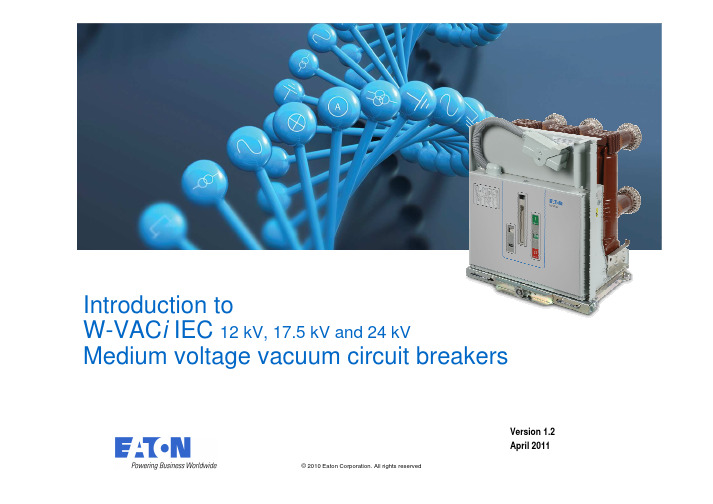
Eaton W-VACi IEC 12 kV、17.5 kV 和 24 kV 中等电压空缸电路断路器
Environmentally friendly design
• Vacuum technology – SF6 gas free • RoHS compliance • Recyclable materials
13
13
W-VACi building blocks
►+ ►
Vacuum interrupters Encapsulated pole unit Universal mechanism
(VI)
(EPU)
assembly (UMA)
W-VACi vacuum circuit breaker
Each building block offers a set of specific benefits to construct a circuit breaker assembly of extreme safety, reliability and performance
• Electrical • Aerospace • Hydraulics • Vehicle
5
5
The electrical power system
Over time, the power system evolves
• Business needs change. Technology is introduced.
• Honored among Ethisphere Institute’s “World’s Most Ethical Companies” for fourth consecutive year
CS5171GDR8中文资料

CS5171, CS5172, CS5173, CS51741.5 A 280 kHz/560 kHz Boost RegulatorsThe CS5171/2/3/4 products are 280 kHz/560 kHz switching regulators with a high efficiency, 1.5 A integrated switch. These partsoperate over a wide input voltage range, from 2.7 V to 30 V. The flexibility of the design allows the chips to operate in most power supply configurations, including boost, flyback, forward, inverting, and SEPIC. The ICs utilize current mode architecture, which allows excellent load and line regulation, as well as a practical means for limiting current. Combining high frequency operation with a highly integrated regulator circuit results in an extremely compact power supply solution. The circuit design includes provisions for features such as frequency synchronization, shutdown, and feedback controls for either positive or negative voltage regulation. These parts are pin−to−pin compatible with LT1372/1373.Features•Pb−Free Packages are Available•Integrated Power Switch: 1.5 A Guaranteed•Wide Input Range: 2.7 V to 30 V•High Frequency Allows for Small Components•Minimum External Components•Easy External Synchronization•Built in Overcurrent Protection•Frequency Foldback Reduces Component Stress During an Overcurrent Condition•Thermal Shutdown with Hysteresis•Regulates Either Positive or Negative Output V oltages•Shut Down Current: 50 m A Maximum•Pin−to−Pin Compatible with LT1372/1373•Wide Temperature Range♦Industrial Grade: −40°C to 125°C♦Commercial Grade: 0°C to 125°CORDERING INFORMATIONSee detailed ordering and shipping information in the package dimensions section on page 17 of this data sheet.5 VSS3.3 VFigure 1. Applications DiagramMAXIMUM RATINGSvalues (not normal operating conditions) and are not valid simultaneously. If these limits are exceeded, device functional operation is not implied, damage may occur and reliability may be affected.1.60 second maximum above 183°C.MAXIMUM RATINGSELECTRICAL CHARACTERISTICS (2.7 V< V CC < 30 V; Industrial Grade: −40°C < T J < 125°C; Commercial Grade: 0°C < T < 125°C; For all CS5171/2/3/4 specifications unless otherwise stated.)Positive and Negative Error AmplifiersOscillatorSync/ Shutdown2.Guaranteed by design, not 100% tested in production.ELECTRICAL CHARACTERISTICS (continued) (2.7 V< V CC < 30 V; Industrial Grade: −40°C < T J < 125°C;Commercial Grade: 0°C < T< 125°C; For all CS5171/2/3/4 specifications unless otherwise stated.)Power SwitchGeneral3.Guaranteed by design, not 100% tested in production.PACKAGE PIN DESCRIPTIONPGNDV SWCFigure 2. Block DiagramTemperature (°C)Figure 3. I CC (No Switching) vs. Temperature C u r r e n t (m A )Temperature (°C)Figure 4. D I CC / D IV SW vs. Temperature(m A /A )I SW (mA)Figure 5. V CE(SAT) vs. I SWV C E (S A T ) (m V )120010008006004002000Temperature (°C)Figure 6. Minimum Input Voltage vs. TemperatureV I N (V )1.51.61.71.81.9010050Temperature (°C)Figure 7. Switching Frequency vs. Temperature(CS5171/2 only)f O S C (k H z )255260265270275010050280285Temperature (°C)Figure 8. Switching Frequency vs. Temperature(CS5173/4 only)f O S C (k H z )5405455505555600565570535530525520Temperature (°C)V o l t a g e (V )Temperature (°C)Temperature (°C)I F B (m A )0.080.100.120.140.160100500.180.20V CC = 12 VV CC = 2.7 VV FB (mV)f O S C (% o f T y p i c a l )V NFB (mV)f O S C (% o f T y p i c a l )Temperature (°C)I N F B (m A )−7−8−10050−9−11−12−13−14Figure 9. Switching Frequency vs. V FB(CS5171/3 only)Figure 10. Switching Frequency vs. V NFB(CS5172/4 only)Figure 11. Reference Voltage vs. Temperature(CS5171/3 only)Figure 12. Reference Voltage vs. Temperature(CS5172/4 only)Figure 13. I FB vs. Temperature (CS5171/3 only)Figure 14. I NFB vs. Temperature (CS5172/ 4 only)V o l t a g e (V )0.50.60.70.80.91.01.10.4C u r r e n t (A )Temperature (°C)D e l a y (m s )801001201401606040D u t y C y c l e (%)V SS (V)I S S (m A )Temperature (°C)V o l t a g e (V )Figure 17. V C Threshold and High ClampVoltage vs. TemperatureFigure 19. Shutdown Delay vs. TemperatureFigure 20. I SS vs. V SSV IN (V)I C C (m A )V REF − V FB (mV)I O U T (m A )20601000−20−6025−25−75Temperature (°C)g m (m m h o )450500550600V REF − V NFB (mV)I O U T (m A )20601000−20−60−100−150−20080400−40Temperature (°C)g m (m m h o )16017050180190150140130120110100Temperature (°C)C u r r e n t (m A )2.62.52.42.32.22.12.0Figure 21. I CC vs. V IN During ShutdownFigure 22. Error Amplifier Transconductancevs. Temperature (CS5171/3 only)Figure 23. Negative Error AmplifierTransconductance vs. Temperature (CS5172/4 only)Figure 24. Error Amplifier I OUT vs. V FB(CS5171/3 only)Figure 25. Error Amplifier I OUT vs. V NFB(CS5172/4 only)Figure 26. Switch Leakage vs. TemperatureAPPLICATIONS INFORMATIONTHEORY OF OPERATIONCurrent Mode ControlLOADFigure 27. Current Mode Control SchemeThe CS517x family incorporates a current mode control scheme, in which the PWM ramp signal is derived from the power switch current. This ramp signal is compared to the output of the error amplifier to control the on−time of the power switch. The oscillator is used as a fixed−frequency clock to ensure a constant operational frequency. The resulting control scheme features several advantages over conventional voltage mode control. First, derived directly from the inductor, the ramp signal responds immediately to line voltage changes. This eliminates the delay caused by the output filter and error amplifier, which is commonly found in voltage mode controllers. The second benefit comes from inherent pulse−by−pulse current limiting by merely clamping the peak switching current. Finally, since current mode commands an output current rather than voltage, the filter offers only a single pole to the feedback loop. This allows both a simpler compensation and a higher gain−bandwidth over a comparable voltage mode circuit.Without discrediting its apparent merits, current mode control comes with its own peculiar problems, mainly,subharmonic oscillation at duty cycles over 50%. The CS517x family solves this problem by adopting a slope compensation scheme in which a fixed ramp generated by the oscillator is added to the current ramp. A proper slope rate is provided to improve circuit stability without sacrificing the advantages of current mode control.Oscillator and ShutdownFigure 28. Timing Diagram of Sync and ShutdownV SWCurrent Ramp Sync The oscillator is trimmed to guarantee an 18% frequency accuracy. The output of the oscillator turns on the power switch at a frequency of 280 kHz (CS5171/2) or 560 kHz (CS5173/4), as shown in Figure 27. The power switch is turned off by the output of the PWM Comparator.A TTL−compatible sync input at the SS pin is capable of syncing up to 1.8 times the base oscillator frequency. As shown in Figure 28, in order to sync to a higher frequency,a positive transition turns on the power switch before the output of the oscillator goes high, thereby resetting the oscillator. The sync operation allows multiple power supplies to operate at the same frequency.A sustained logic low at the SS pin will shut down the IC and reduce the supply current.An additional feature includes frequency shift to 20% of the nominal frequency when either the NFB or FB pins trigger the threshold. During power up, overload, or short circuit conditions, the minimum switch on−time is limited by the PWM comparator minimum pulse width. Extra switch off−time reduces the minimum duty cycle to protect external components and the IC itself.As previously mentioned, this block also produces a ramp for the slope compensation to improve regulator stability.Error AmplifierFigure 29. Error Amplifier Equivalent CircuitFBNFBWm F For CS5172/4, the NFB pin is internally referenced to −2.5 V with approximately a 250 k W input impedance. For CS5171/3, the FB pin is directly connected to the inverting input of the positive error amplifier, whose non−inverting input is fed by the 1.276 V reference. Both amplifiers are transconductance amplifiers with a high output impedance of approximately 1 M W , as shown in Figure 29. The V C pin is connected to the output of the error amplifiers and is internally clamped between 0.5 V and 1.7 V . A typical connection at the V C pin includes a capacitor in series with a resistor to ground, forming a pole/zero for loop compensation.An external shunt can be connected between the V C pin and ground to reduce its clamp voltage. Consequently, the current limit of the internal power transistor current is reduced from its nominal value.Switch Driver and Power SwitchThe switch driver receives a control signal from the logic section to drive the output power switch. The switch is grounded through emitter resistors (63 m W total) to the PGND pin. PGND is not connected to the IC substrate so that switching noise can be isolated from the analog ground. The peak switching current is clamped by an internal circuit. The clamp current is guaranteed to be greater than 1.5 A and varies with duty cycle due to slope compensation. The power switch can withstand a maximum voltage of 40 V on the collector (V SW pin). The saturation voltage of the switch is typically less than 1 V to minimize power dissipation.Short Circuit ConditionWhen a short circuit condition happens in a boost circuit,the inductor current will increase during the whole switching cycle, causing excessive current to be drawn from the input power supply. Since control ICs don’t have the means to limit load current, an external current limit circuit (such as a fuse or relay) has to be implemented to protect the load, power supply and ICs.In other topologies, the frequency shift built into the IC prevents damage to the chip and external components. This feature reduces the minimum duty cycle and allows the transformer secondary to absorb excess energy before the switch turns back on.Figure 30. Startup Waveforms of Circuit Shown inthe Application Diagram. Load = 400 mA.I LV OUT V CV CCThe CS517x can be activated by either connecting the V CC pin to a voltage source or by enabling the SS pin.Startup waveforms shown in Figure 30 are measured in the boost converter demonstrated in the Application Diagram on the page 2 of this document. Recorded after the input voltage is turned on, this waveform shows the various phases during the power up transition.When the V CC voltage is below the minimum supply voltage, the V SW pin is in high impedance. Therefore,current conducts directly from the input power source to the output through the inductor and diode. Once V CC reachesapproximately 1.5 V , the internal power switch briefly turns on. This is a part of the CS517x’s normal operation. The turn−on of the power switch accounts for the initial current swing.When the V C pin voltage rises above the threshold, the internal power switch starts to switch and a voltage pulse can be seen at the V SW pin. Detecting a low output voltage at the FB pin, the built−in frequency shift feature reduces the switching frequency to a fraction of its nominal value,reducing the minimum duty cycle, which is otherwise limited by the minimum on−time of the switch. The peak current during this phase is clamped by the internal current limit.When the FB pin voltage rises above 0.4 V , the frequency increases to its nominal value, and the peak current begins to decrease as the output approaches the regulation voltage.The overshoot of the output voltage is prevented by the active pull−on, by which the sink current of the error amplifier is increased once an overvoltage condition is detected. The overvoltage condition is defined as when the FB pin voltage is 50 mV greater than the reference PONENT SELECTIONFrequency CompensationThe goal of frequency compensation is to achieve desirable transient response and DC regulation while ensuring the stability of the system. A typical compensation network, as shown in Figure 31, provides a frequency response of two poles and one zero. This frequency response is further illustrated in the Bode plot shown in Figure 32.Figure 31. A Typical Compensation NetworkC2The high DC gain in Figure 32 is desirable for achieving DC accuracy over line and load variations. The DC gain of a transconductance error amplifier can be calculated as follows:Gain DC +G M R Owhere:G M = error amplifier transconductance;R O = error amplifier output resistance ≈ 1 M W .The low frequency pole, f P1, is determined by the error amplifier output resistance and C1 as:f P1+1OThe first zero generated by C1 and R1 is:f Z1+1The phase lead provided by this zero ensures that the loop has at least a 45° phase margin at the crossover frequency.Therefore, this zero should be placed close to the pole generated in the power stage which can be identified at frequency:f P +12p C O R LOADwhere:C O = equivalent output capacitance of the error amplifier ≈120pF;R LOAD = load resistance.The high frequency pole, f P2, can be placed at the output filter’s ESR zero or at half the switching frequency. Placing the pole at this frequency will cut down on switching noise.The frequency of this pole is determined by the value of C2and R1:f P2+12p C2R1One simple method to ensure adequate phase margin is todesign the frequency response with a −20 dB per decade slope, until unity−gain crossover. The crossover frequency should be selected at the midpoint between f Z1 and f P2 wherethe phase margin is maximized.Figure 32. Bode Plot of the Compensation NetworkShown in Figure 31Frequency (LOG)G a i n (d B )Negative Voltage FeedbackSince the negative error amplifier has finite input impedance as shown in Figure 33, its induced error has to be considered. If a voltage divider is used to scale down the negative output voltage for the NFB pin, the equation for calculating output voltage is:*V OUT +ǒ*2.5(R1)R2)R2Ǔ*10m A R1Figure 33. Negative Error Amplifier and NFB PinIt is shown that if R1 is less than 10 k, the deviation from the design target will be less than 0.1 V . If the tolerances of the negative voltage reference and NFB pin input current are considered, the possible offset of the output V OFFSET varies in the range of:ǒ*0.0.5(R1)R2)R2Ǔ*(15m A R1)v V OFFSETv ǒ0.0.5(R1)R2)Ǔ*(5m A R1)V SW Voltage LimitIn the boost topology, V SW pin maximum voltage is set by the maximum output voltage plus the output diode forward voltage. The diode forward voltage is typically 0.5 V for Schottky diodes and 0.8 V for ultrafast recovery diodesV SW(MAX)+V OUT(MAX))V Fwhere:V F = output diode forward voltage.In the flyback topology, peak V SW voltage is governed by:V SW(MAX)+V CC(MAX))(V OUT )V F ) Nwhere:N = transformer turns ratio, primary over secondary.When the power switch turns off, there exists a voltage spike superimposed on top of the steady−state ually this voltage spike is caused by transformer leakage inductance charging stray capacitance between the V SW and PGND pins. To prevent the voltage at the V SW pin from exceeding the maximum rating, a transient voltage suppressor in series with a diode is paralleled with the primary windings. Another method of clamping switch voltage is to connect a transient voltage suppressor between the V SW pin and ground.Magnetic Component SelectionWhen choosing a magnetic component, one must consider factors such as peak current, core and ferrite material, output voltage ripple, EMI, temperature range, physical size and cost. In boost circuits, the average inductor current is the product of output current and voltage gain (V OUT /V CC ),assuming 100% energy transfer efficiency. In continuous conduction mode, inductor ripple current isI RIPPLE +V CC (V OUT*V CC )OUT)where:f = 280 kHz for CS5171/2 and 560 kHz for CS5173/4.The peak inductor current is equal to average current plus half of the ripple current, which should not cause inductor saturation. The above equation can also be referenced when selecting the value of the inductor based on the tolerance of the ripple current in the circuits. Small ripple current provides the benefits of small input capacitors and greater output current capability. A core geometry like a rod or barrel is prone to generating high magnetic field radiation,but is relatively cheap and small. Other core geometries,such as toroids, provide a closed magnetic loop to prevent EMI.Input Capacitor SelectionIn boost circuits, the inductor becomes part of the input filter, as shown in Figure 35. In continuous mode, the input current waveform is triangular and does not contain a large pulsed current, as shown in Figure 34. This reduces the requirements imposed on the input capacitor selection.During continuous conduction mode, the peak to peak inductor ripple current is given in the previous section. As we can see from Figure 34, the product of the inductor current ripple and the input capacitor’s effective series resistance (ESR) determine the V CC ripple. In most applications, input capacitors in the range of 10 m F to 100 m F with an ESR less than 0.3 W work well up to a full 1.5 A switch current.V CC rippleFigure 34. Boost Input Voltage and CurrentRipple WaveformsI INI LFigure 35. Boost Circuit Effective Input FilterV CCI The situation is different in a flyback circuit. The input current is discontinuous and a significant pulsed current is seen by the input capacitors. Therefore, there are two requirements for capacitors in a flyback regulator: energy storage and filtering. To maintain a stable voltage supply to the chip, a storage capacitor larger than 20 m F with low ESR is required. To reduce the noise generated by the inductor,insert a 1.0 m F ceramic capacitor between V CC and ground as close as possible to the chip.Output Capacitor SelectionFigure 36. Typical Output Voltage RippleV OUT rippleI LBy examining the waveforms shown in Figure 36, we can see that the output voltage ripple comes from two major sources, namely capacitor ESR and the charging/discharging of the output capacitor. In boost circuits, when the power switch turns off, I L flows into the output capacitor causing an instant D V = I IN × ESR. At the same time, current I L − I OUT charges the capacitor and increases the output voltage gradually. When the power switch is turned on, I L is shunted to ground and I OUT discharges the output capacitor. When the I L ripple is small enough, I L can be treated as a constant and is equal to input current I IN .Summing up, the output voltage peak−peak ripple can be calculated by:V OUT(RIPPLE)+(I IN*I OUT)(1*D)(C OUT)(f))I OUT DOUT)I IN ESRThe equation can be expressed more conveniently in terms of V CC, V OUT and I OUT for design purposes as follows:V OUT(RIPPLE)+I OUT(V OUT*V CC)(C OUT)(f)1(C OUT)(f))(I OUT)(V OUT)(ESR)V CCThe capacitor RMS ripple current is:I RIPPLE+(I IN*I OUT)2(1*D))(I OUT)2(D)Ǹ+I OUT V OUT *V CCV CCǸAlthough the above equations apply only for boost circuits, similar equations can be derived for flyback circuits.Reducing the Current LimitIn some applications, the designer may prefer a lower limit on the switch current than 1.5 A. An external shunt can be connected between the V C pin and ground to reduce its clamp voltage. Consequently, the current limit of the internal power transistor current is reduced from its nominal value.The voltage on the V C pin can be evaluated with the equationV C+I SW R E A Vwhere:R E = .063W, the value of the internal emitter resistor;A V = 5 V/V, the gain of the current sense amplifier. Since R E and A V cannot be changed by the end user, the only available method for limiting switch current below 1.5 A is to clamp the V C pin at a lower voltage. If the maximum switch or inductor current is substituted into the equation above, the desired clamp voltage will result.A simple diode clamp, as shown in Figure 37, clamps the V C voltage to a diode drop above the voltage on resistor R3.Unfortunately, such a simple circuit is not generally acceptable if V INis loosely regulated.Figure 37. Current Limiting using a Diode Clamp V INAnother solution to the current limiting problem is to externally measure the current through the switch using a sense resistor. Such a circuit is illustrated in Figure 38.Figure 38. Current Limiting using a Current SenseResistorVOutputGround The switch current is limited toI SWITCH(PEAK)+V BE(Q1)SENSEwhere:V BE(Q1) = the base−emitter voltage drop of Q1, typically 0.65 V.The improved circuit does not require a regulated voltage to operate properly. Unfortunately, a price must be paid for this convenience in the overall efficiency of the circuit. The designer should note that the input and output grounds are no longer common. Also, the addition of the current sense resistor, R SENSE , results in a considerable power loss which increases with the duty cycle. Resistor R2 and capacitor C3form a low−pass filter to remove noise.Subharmonic OscillationSubharmonic oscillation (SHM) is a problem found in current−mode control systems, where instability results when duty cycle exceeds 50%. SHM only occurs in switching regulators with a continuous inductor current.This instability is not harmful to the converter and usually does not affect the output voltage regulation. SHM will increase the radiated EM noise from the converter and can cause, under certain circumstances, the inductor to emit high−frequency audible noise.SHM is an easily remedied problem. The rising slope of the inductor current is supplemented with internal “slope compensation” to prevent any duty cycle instability from carrying through to the next switching cycle. In the CS517x family, slope compensation is added during the entire switch on−time, typically in the amount of 180 mA/m s.In some cases, SHM can rear its ugly head despite the presence of the onboard slope compensation. The simple cure to this problem is more slope compensation to avoid the unwanted oscillation. In that case, an external circuit, shown in Figure 39, can be added to increase the amount of slope compensation used. This circuit requires only a few components and is “tacked on” to the compensationnetwork.Figure 39. Technique for Increasing SlopeCompensationSWThe dashed box contains the normal compensation circuitry to limit the bandwidth of the error amplifier.Resistors R2 and R3 form a voltage divider off of the V SW pin. In normal operation, V SW looks similar to a square wave, and is dependent on the converter topology. Formulas for calculating V SW in the boost and flyback topologies are given in the section “V SW V oltage Limit.” The voltage on V SW charges capacitor C3 when the switch is off, causing the voltage at the V C pin to shift upwards. When the switch turns on, C3 discharges through R3, producing a negative slope at the V C pin. This negative slope provides the slope compensation.The amount of slope compensation added by this circuit isD I D T+VSW ǒR 3R 2)R 3Ǔǒ1*e*(1*D)R 3C 3f SW Ǔǒf SW (1*D)R E A VǓwhere:D I/D T = the amount of slope compensation added (A/s);V SW = the voltage at the switch node when the transistor is turned off (V);f SW = the switching frequency, typically 280 kHz (CS5171/3) or 560 kHz (CS5172/4) (Hz);D = the duty cycle;R E = 0.063 W , the value of the internal emitter resistor;A V = 5 V/V , the gain of the current sense amplifier.In selecting appropriate values for the slope compensation network, the designer is advised to choose a convenient capacitor, then select values for R2 and R3 such that the amount of slope compensation added is 100 mA/m s. Then R2 may be increased or decreased as necessary. Of course,the series combination of R2 and R3 should be large enough to avoid drawing excessive current from V SW . Additionally,to ensure that the control loop stability is improved , the time constant formed by the additional components should be chosen such thatR 3C 3t 1*Df SWFinally, it is worth mentioning that the added slope compensation is a tradeoff between duty cycle stability and transient response. The more slope compensation a designer adds, the slower the transient response will be, due to the external circuitry interfering with the proper operation of the error amplifier.Soft−StartThrough the addition of an external circuit, a Soft−Start function can be added to the CS5171/2/3/4 family of components. Soft−Start circuitry prevents the V C pin from slamming high during startup, thereby inhibiting the inductor current from rising at a high slope.This circuit, shown in Figure 40, requires a minimum number of components and allows the Soft−Start circuitry toactivate any time the SS pin is used to restart the converter.Figure 40. Soft StartV INSSResistor R1 and capacitors C1 and C2 form the compensation network. At turn on, the voltage at the V C pin starts to come up, charging capacitor C3 through Schottky diode D2, clamping the voltage at the V C pin such that switching begins when V C reaches the V C threshold,typically 1.05 V (refer to graphs for detail over temperature).V C +V F(D2))V C3Therefore, C3 slows the startup of the circuit by limiting the voltage on the V C pin. The Soft−Start time increases with the size of C3.Diode D1 discharges C3 when SS is low. If the shutdown function is not used with this part, the cathode of D1 should be connected to V IN .Calculating Junction TemperatureTo ensure safe operation of the CS5171/2/3/4, the designer must calculate the on−chip power dissipation and determine its expected junction temperature. Internal thermal protection circuitry will turn the part off once the junction temperature exceeds 180°C ±30°. However,repeated operation at such high temperatures will ensure a reduced operating life.Calculation of the junction temperature is an imprecise but simple task. First, the power losses must be quantified.There are three major sources of power loss on the CS517x:•biasing of internal control circuitry, P BIAS •switch driver, P DRIVER •switch saturation, P SATThe internal control circuitry, including the oscillator and linear regulator, requires a small amount of power evenwhen the switch is turned off. The specifications section of this datasheet reveals that the typical operating current, I Q ,due to this circuitry is 5.5 mA. Additional guidance can be found in the graph of operating current vs. temperature. This graph shows that IQ is strongly dependent on input voltage,V IN , and temperature. ThenP BIAS +V IN I QSince the onboard switch is an NPN transistor, the base drive current must be factored in as well. This current is drawn from the V IN pin, in addition to the control circuitry current. The base drive current is listed in the specifications as D I CC /D I SW , or switch transconductance. As before, the designer will find additional guidance in the graphs. With that information, the designer can calculateP DRIVER +V IN I SW ICC D I SWDwhere:I SW = the current through the switch;D = the duty cycle or percentage of switch on−time.I SW and D are dependent on the type of converter. In a boost converter,I SW(AVG)^I LOAD D1EfficiencyD ^V OUT*V IN V OUTIn a flyback converter,I SW(AVG)^V OUT I LOAD V IN1Efficiency D ^V OUT V OUT )NSN P V INThe switch saturation voltage, V (CE)SAT , is the last major source of on−chip power loss. V (CE)SAT is the collector−emitter voltage of the internal NPN transistor when it is driven into saturation by its base drive current. The value for V (CE)SAT can be obtained from the specifications or from the graphs, as “Switch Saturation V oltage.” Thus,P SAT ^V (CE)SAT I SW DFinally, the total on−chip power losses areP D +P BIAS )P DRIVER )P SATPower dissipation in a semiconductor device results in the generation of heat in the junctions at the surface of the chip.This heat is transferred to the surface of the IC package, but a thermal gradient exists due to the resistive properties of the package molding compound. The magnitude of the thermal gradient is expressed in manufacturers’ data sheets as q JA ,or junction−to−ambient thermal resistance. The on−chip junction temperature can be calculated if q JA , the air temperature near the surface of the IC, and the on−chip power dissipation are known.。
麦克维尔产品手册
750
800
800
850
850
900
950
1000
1100
1200
1300
输入功率
kW
447.3
462
489.1
504.5
518.5
526.4
558.4
587.5
619.9
680.1
759
824.7
电源
380V/3N〜/50Hz
注:■ 以上选型适用于冷冻水进/出水温度为 12℃/7℃,冷却水进/出水温度为 32℃/37℃,换热器流程数为 2 流程。
40 热泵热水机组
模块式空气源热泵热水机组MHA
42 末端空调机组
组合式空气处理机组 MDM 洁净室用空气调节机组 MDX 单壁柜式空气处理机组 MSW 双壁柜式空气处理机组 MDW 超薄吊顶式空气处理机组 MHW 卧式暗装风机盘管 MCW 立式暗装风机盘管 MFCW 立式明装风机盘管 MFMW 天花嵌入式风机盘管 MCKW 卧式明装风机盘管 MCMW 吊顶式全热热回收新风机组 HRB
79 轻型商用空调机组
天花嵌入式分体空调器 MCK-T 明装吊顶/座地式分体空调器 MCM-D 暗装吊顶式分体空调机组 MCC-T 风冷冷风/热泵型管道式空调机 MDB“T”系列 风冷冷风/热泵型管道式空调机 MDB“M”系列 风冷冷风/热泵型管道式空调机 MDB“S”系列 “旋风”系列水冷柜机 MWCP 屋顶式空调机组 MRT
PC5171B-12ST中文资料
Automotive Subminiatur e PCB Power RelayFEATURES15 Amp continuous current cap acity Up to 60 amp switching capaci ty Four different contact materials available Six different contact formsDesigned for high inrush applic ations UL Class F insulation standardPC517Dust cover or sealed version a vailableFormMax Switching Current Minimum Load1 Form A 60 Amps 20 Amps 1 Form B 12 Amps 10 Amps 10 Amps1 Form C (DPDT)NO NC CONTACT RATINGSCONTACT DATAMaterialInitial Contact Resistance Service LifeMechanical ElectricalAgNiO 15 (Silver Nickel Oxide 15%), AgSnOInO (Silver Tin Oxide Indium Oxide)100 milliohms max @ 0.1A, 6VDC 1 X 1072 X 10515 AmpsOperations OperationsSales: Call Toll Free (888)997-3933 Fax (818) 342-5296 email: pickerwest@ URL: 3220 Commander Drive, Suite 102, Carrollton, T exas 75006(SPST NC)PC517 Rev B 4-14-04PAGE 1(SPST NO)Make Motor60 Amps 20 Amps 15 Amps12 Amps 10 Amps 10 Amps.05 Amps @ 5 VDC1 Form U1 Form V 1 Form W (SPDT-DB-DM)2 X 40 Amps 2 X 20 Amps 2 X 10 Amps 2 X 8 Amps 2 X 7 Amps 2 X 7 AmpsNO NC 2 X 30 Amps 2 X 15 Amps 2 X 7 Amps2 X 5 Amps 2 X 5 Amps 2 X 5 Amps(SPST-NO-DM)(SPST-NC-DB)Max. Continuous Current See curve page 2, current dependantMax. Switching VoltageCHARACTERISTICSOperate Time 3 ms. typical Release Time Insulation Resistance 1.5 ms. typical100 megohms min, at 500VDC, 50%RH Dielectric Strength 500 Vrms, 1 min. between coil and contacts Shock Resistance 10 g, 11ms, functional; 100 g, destructive Vibration Resistance DA 1.5 mm, 20 - 200 Hz functionalPower Consumption 1.1 W approx.Ambient Temperature Range -40 to 85 degrees C operating, -40 to 155 stora ge WeightOpen: 8 grams; Enclosed: 12 grams approx.Drop Resistance 1 Meter height drop on concrete in final enclosu re COIL DATAPC517PC517Sales: Call Toll Free (888) 997-3933 F ax (818) 342-5296 email: pickerwest@sbc URL: 3220 Commander Drive, Suite 102, Car rollton, Texas 75006PAGE 2Tolerances +.010 unless otherwise notedNotes:Contact Form W shownOn other contact forms Unused Pins are OmittedDimensions in Inches (millimet ers) drawings are 2 X scaleSide View End ViewBottom View PC Board Layout REFERENCE CURVESORDERING INFORMATIONExample:PC517Model-1CContact FormContact Material-12Nil: AgSnO; C: AgCdO; T: AgSnOInOCoil VoltageSNil: Open Frame; S: Sealed; C: Dust Cover EnclosureT1A, 1B, 1C, 1U, 1V or 1W (8.89).35.15(3.81)(10.16).40(1.8).070(17.7).697(15.2).598(19.7).776(3.5).138Maximum make current refers to inruch current of a lamp load。
无级调温器[实用新型专利]
![无级调温器[实用新型专利]](https://img.taocdn.com/s3/m/683fa3e8a6c30c2258019e0e.png)
专利名称:无级调温器
专利类型:实用新型专利
发明人:雷雨成,梁华声,江冠龙申请号:CN97210396.1
申请日:19970526
公开号:CN2301633Y
公开日:
19981223
专利内容由知识产权出版社提供
摘要:本实用新型属于一种与厨房电热器具配套的无级调温器,它采用一个独立的控制盒,在控制盒内设置了电位器、按钮、电源输出插座及散热器、控制电路板等,由整流稳压、功率调整、断电保护等单元电路组成控制电路,本实用新型结构紧凑,使用安全,方便可靠,节能省电,负载能力强,适用于对使用电热元件的电器产品进行功率变化或温度调节。
申请人:四川省乐山市五通桥锅厂
地址:614800 四川省乐山市五通桥区佑君街
国籍:CN
代理机构:乐山市专利事务所
代理人:叶建民
更多信息请下载全文后查看。
2SC5171中文资料(toshiba)中文数据手册「EasyDatasheet - 矽搜」
2SC5171
Min Typ. Max Unit
― ― 5.0 µA
― ― 5.0 µA
180 ―
―
V
100 ― 320
50 ― ―
― 0.16 1.0
V
― 0.68 1.5
V
― 200 ― MHz
― 16 ― pF
C5171
部件号(或缩写代码) 批号
A线指示铅(Pb)free包装或铅(Pb)-free完 成.
• 此处所包含的信息如有更改,恕不另行通知.
• 本文所含信息仅显示为对我们产品的应用指南.否
承担因东芝专利或其它第三方权利的任何侵犯其
可能导致其使用.没有获发牌照以暗示或以其他方式在任何专利或专利的权利 东芝或其它.
• 东芝正在不断努力提高其产品的质量和可靠性.然而,在一般情况可能发生故障或失效由于其固有的电灵敏度和易受物理应力的半导 体器件.它是利用东芝产品时,要遵守安全的在制造安全设计为整个系统的标准,以避免情况,其中,例如东芝产品的故障或失灵会引 起人的生命损失买方,负责,人身伤害或财产损失.
芯片中文手册,看全文,戳
2SC5171
功率放大器应用 驱动级放大器的应用
2SC5171
单位:mm
• 高转换频率:F • 为了补充2SA1930
T = 200 MHz(典型值).
绝对最大额定值
( TC = 25℃)
特点
符
评级
Unit
集电极基极电压
VCBO
180
V
集电极 - 发射极电压
2
2006-11-10
芯片中文手册,看全文,戳
2SC5171
2.0 150
100 1.6
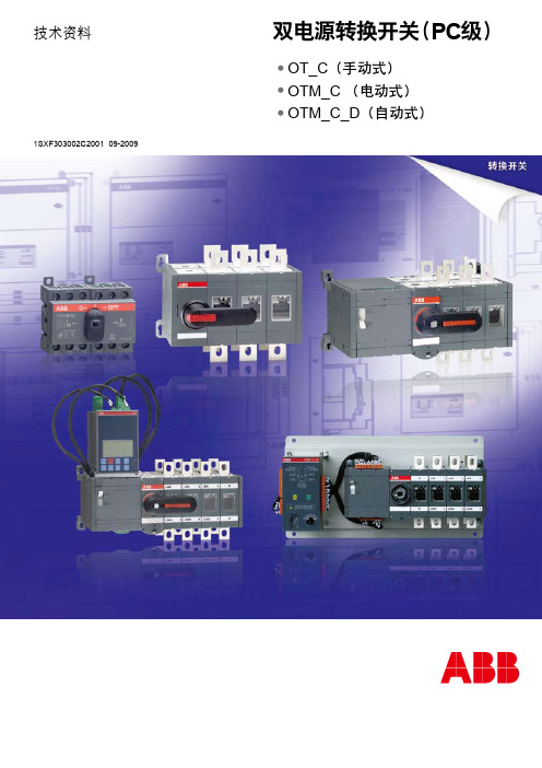
双电源转换开关-PC级
- 1、下载文档前请自行甄别文档内容的完整性,平台不提供额外的编辑、内容补充、找答案等附加服务。
- 2、"仅部分预览"的文档,不可在线预览部分如存在完整性等问题,可反馈申请退款(可完整预览的文档不适用该条件!)。
- 3、如文档侵犯您的权益,请联系客服反馈,我们会尽快为您处理(人工客服工作时间:9:00-18:30)。
Automotive Subminiatur e PCB Power Relay
FEATURES
15 Amp continuous current cap acity Up to 60 amp switching capaci ty Four different contact materials available Six different contact forms
Designed for high inrush applic ations UL Class F insulation standard
PC517
Dust cover or sealed version a vailable
Form
Max Switching Current Minimum Load
1 Form A 60 Amps 20 Amps 1 Form B 1
2 Amps 10 Amps 10 Amps
1 Form C (DPDT)NO NC CONTACT RATINGS
CONTACT DATA
Material
Initial Contact Resistance Service Life
Mechanical Electrical
AgNiO 15 (Silver Nickel Oxide 15%), AgSnOInO (Silver Tin Oxide Indium Oxide)100 milliohms max @ 0.1A, 6VDC 1 X 1072 X 105
15 Amps
Operations Operations
Sales: Call Toll Free (888)997-3933 Fax (818) 342-5296 email: pickerwest@ URL:
3220 Commander Drive, Suite 102, Carrollton, T exas 75006
(SPST NC)PC517 Rev B 4-14-04
PAGE 1
(SPST NO)Make Motor
60 Amps 20 Amps 15 Amps
12 Amps 10 Amps 10 Amps
.05 Amps @ 5 VDC
1 Form U
1 Form V 1 Form W (SPDT-DB-DM)
2 X 40 Amps 2 X 20 Amps 2 X 10 Amps 2 X 8 Amps 2 X 7 Amps 2 X 7 Amps
NO NC 2 X 30 Amps 2 X 15 Amps 2 X 7 Amps
2 X 5 Amps 2 X 5 Amps 2 X 5 Amps
(SPST-NO-DM)(SPST-NC-DB)
Max. Continuous Current See curve page 2, current dependant
Max. Switching Voltage
CHARACTERISTICS
Operate Time 3 ms. typical Release Time Insulation Resistance 1.5 ms. typical
100 megohms min, at 500VDC, 50%RH Dielectric Strength 500 Vrms, 1 min. between coil and contacts Shock Resistance 10 g, 11ms, functional; 100 g, destructive Vibration Resistance DA 1.5 mm, 20 - 200 Hz functional
Power Consumption 1.1 W approx.
Ambient Temperature Range -40 to 85 degrees C operating, -40 to 155 stora ge Weight
Open: 8 grams; Enclosed: 12 grams approx.
Drop Resistance 1 Meter height drop on concrete in final enclosu re COIL DATA
PC517
PC517
Sales: Call Toll Free (888) 997-3933 F ax (818) 342-5296 email: pickerwest@sbc URL:
3220 Commander Drive, Suite 102, Car rollton, Texas 75006
PAGE 2
Tolerances +.010 unless otherwise noted
Notes:
Contact Form W shown
On other contact forms Unused Pins are Omitted
Dimensions in Inches (millimet ers) drawings are 2 X scale
Side View End View
Bottom View PC Board Layout REFERENCE CURVES
ORDERING INFORMATION
Example:
PC517
Model
-1C
Contact Form
Contact Material
-12
Nil: AgSnO; C: AgCdO; T: AgSnOInO
Coil Voltage
S
Nil: Open Frame; S: Sealed; C: Dust Cover Enclosure
T
1A, 1B, 1C, 1U, 1V or 1W (8.89)
.35.15(3.81)
(10.16)
.40(1.8)
.070(17.7)
.697
(15.2)
.598
(19.7)
.776(3.5)
.138Maximum make current refers to inruch current of a lamp load。