HZK3LL中文资料
LM3Z2V4T1G中文资料
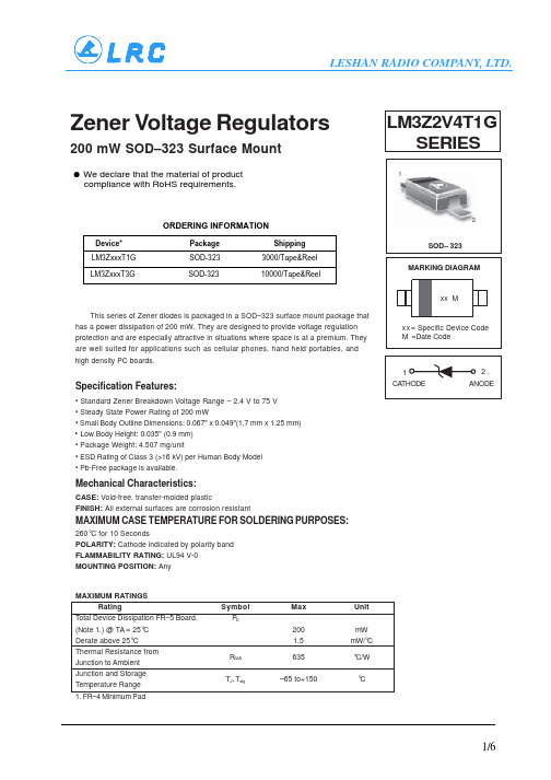
Zener Voltage Regulators200 mW SOD–323 Surface Mount12This series of Zener diodes is packaged in a SOD–323 surface mount package that has a power dissipation of 200 mW. They are designed to provide voltage regulation protection and are especially attractive in situations where space is at a premium. They are well suited for applications such as cellular phones, hand held portables, and high density PC boards.Specification Features:• Standard Zener Breakdown Voltage Range – 2.4 V to 75 V • Steady State Power Rating of 200 mW• Small Body Outline Dimensions: 0.067" x 0.049"(1.7 mm x 1.25 mm).Low Body Height: 0.035" (0.9 mm)• Package Weight: 4.507 mg/unit• ESD Rating of Class 3 (>16 kV) per Human Body Model • Pb-Free package is available.Mechanical Characteristics:CASE:Void-free, transfer-molded plasticFINISH:All external surfaces are corrosion resistantMAXIMUM CASE TEMPERATURE FOR SOLDERING PURPOSES:260°C for 10 SecondsPOLARITY:Cathode indicated by polarity band FLAMMABILITY RATING: UL94 V-0MOUNTING POSITION: AnyMAXIMUM RATINGSRatingSymbol Max Unit Total Device Dissipation FR–5 Board,P D(Note 1.) @ TA = 25°C 200mW Derate above 25°C1.5mW/°C Thermal Resistance from R θJA 635°C/W Junction to AmbientJunction and StorageT J , T stg–65 to+150°CTemperature Range 1. FR–4 Minimum PadORDERING INFORMATIONDevice*Package ShippingLM3ZxxxT1G SOD-3233000/Tape&ReelLM3ZxxxT3GSOD-32310000/Tape&ReelLESHAN RADIO COMPANY, LTD.1/6ƽ We declare that the material of productcompliance with RoHS requirements.LM3Z2V4T1G SERIESELECTRICAL CHARACTERISTICS(T A = 25°C unless otherwise noted,V F = 0.9 V Max. @ I F= 10 mA for all types)Symbol ParameterV Z Reverse Zener Voltage @ I ZT I ZT Reverse CurrentZ ZT Maximum Zener Impedance @ I ZT I ZK Reverse CurrentZ ZK Maximum Zener Impedance @ I ZK I R Reverse Leakage Current @ V R V R Reverse Voltage I F Forward Current V F Forward Voltage @ I FQ V Z Maximum Temperature Coefficient of V Z CMax. Capacitance @V R = 0 and f = 1 MHzLESHAN RADIO COMPANY, LTD.2/6LM3Z2V4T1G SERIES2.Zener voltage is measured with a pulse test current I Z at an ambient temperature of 25°C.LESHAN RADIO COMPANY, LTD.3/6LM3Z2V4T1G SERIESTypical CharacteristicsZ Z T , D Y N A M I C I M P E D A N C E ()Ω1000100101.0C , C A P A C I T A N C E (p F )70V Z , NOMINAL ZENER VOLTAGE (V)Figure 3. Typical Capacitance 104.0V Z , NOMINAL ZENER VOLTAGE (V)Figure 4. Typical Leakage Current70605040302010LESHAN RADIO COMPANY, LTD.4/6LM3Z2V4T1G SERIESTypical Characteristics12V Z , ZENER VOLTAGE (V)100101.00.10.01108.06.04.02.00I Z , Z E N E R C U R R E N T (m A )V Z , ZENER VOLTAGE (V)Figure 5. Zener Voltage versus Zener Current(V Z Up to 12 V)Figure 6. Zener Voltage versus Zener Current(12 V to 75 V)1001010.10.011030507090I Z , Z E N E R C U R R E N T (m A )TEMPERATURE (°C)2501004020PO W E R D I S S I P A T I O N (%)50751001251508060Figure 7. Steady State Power DeratingLESHAN RADIO COMPANY, LTD.5/6PACKAGE DIMENSIONSSOD-323MINMAXMINMAXAB CD E H J K1.601.150.800.250.000.0892.301.801.351.000.400.100.1772.700.0630.0450.0310.0100.00000.00350.0910.0710.0530.0390.0160.0040.00700.106DINMILLIMETERS INCHES0.15 REF 0.006 REF NOTES:1. CONTROLLING DIMENSION: MILLIMETERS2. LEAD THICKNESS SPECIFIED PER L / F DRAWING WITH SOLDER PLATING.DSOD-32312LM3Z2V4T1G SERIESSTYLE 1:PIN 1: CATHODE 2: ANODELESHAN RADIO COMPANY, LTD.6/6Reel DimensionsMetric Dimensions Govern –– English are in parentheses for reference onlyEMBOSSED TAPE AND REEL DATAFOR DISCRETESAT MaxOutside Dimension Measured at EdgeGInside Dimension Measured Near Hub20.2mm Min (.795’’)1.5mm Min(.06’’)13.0mm ± 0.5mm(.512 ±.002’’)50mm Min (1.969’’)Full RadiusSize A Max GT Max 8 mm330mm (12.992’’)8.4mm+1.5mm, -0.0(.33’’+.059’’, -0.00)14.4mm (.56’’)LESHAN RADIO COMPANY, LTD.Storage ConditionsTemperature: 5 to 40 Deg.C (20 to 30 Deg. C is preferred) Humidity: 30 to 80 RH (40 to 60 is preferred )Recommended Period: One year after manufacturing(This recommended period is for the soldering condition only. The characteristics and reliabilities of the products are not restricted to this limitation)元器件交易网Shi p ment S p ecification10 Reel12 Inner Box/Carton 360KPCS/CartonDim(Unit:mm)Dim(Unit:mm)10Reel/Inner Box30KPCS/Inner Box460mm*400mm*420mm8000PCS/Reel (SOT-723,SOD-723)3000PCS/Reel80KPCS/Inner Box (SOT-723,SOD-723)960KPCS/Carton (SOT-723,SOD-723)LESHAN RADIO COMPANY, LTD.元器件交易网。
凯利KBL系列大功率电动汽车 无刷电机控制器用户手册说明书

凯利KBL系列大功率电动汽车无刷电机控制器用户手册适用的产品型号:KBL72601E EKBL36101X X KBL72601KBL24101X X KBL36101KBL24101KBL24151KBL36151X X KBL96151KBL24151X X KBL36151KBL242KBL362221X KBL96201KBL242221X KBL362KBL36301X X KBL96251KBL24301KBL24301X X KBL36301KBL72101X X KBL96351EKBL48101X X KBL72101KBL48101KBL48151X X KBL72151KBL72151X XKBL48151KBL722221XKBL482221X KBL722KBL482KBL72301X XKBL48301X X KBL72301KBL48301KBL72401E EKBL48401KBL48401E E KBL72401KBL48501KBL48501E E KBL72501KBL72501E E版本3.32013年4月目录第一章概述 (2)第二章主要特性和规格 (3)2.1基本功能 (3)2.2特性 (4)2.3规格 (4)2.4型号 (5)第三章安装方法 (5)3.1安装控制器 (5)3.2连线 (8)3.3连接计算机串口 (13)3.4安装时检查 (13)第四章维护 (14)4.1清理 (14)4.2配置 (14)表1:LED错误代码 (15)联系我们: (18)1第一章概述本手册主要介绍凯利公司KBL系列电动车无刷控制器产品的特性,安装使用方法以及维护等方面的知识。
用户在使用凯利控制器之前,请详细阅读本手册,这会帮助您正确的安装和使用凯利控制器。
如果在使用过程中遇到任何问题,请从本文档最后一页查询联系方式与我们联系。
凯利KBL系列电动车控制器是凯利公司为中小型电动车辆提供的一种高效、平稳和容易安装的电动车控制器。
Z-330P2J2;中文规格书,Datasheet资料

Z-330P2J2 xDSL over POTS CPE In-Line FilterZ-330P2J2 block schematicEX132.B (11/10)DescriptionThe Z-330P2J2 is a small, in-line, ANSI T1.421-compliant customer premises equipment (CPE) filter designed to expedite the service delivery and improve the performance of digital subscriber line (DSL) and home phoneline network (HPN) ser-vices over plain old telephone service (POTS). The Z-330P2J2 filters all telephones, facsimile (fax) machines, answering machines, and other telephone equipment. Its third-order filter design electronically isolates the high-speed DSL and HPN data streams from the voice-band POTS to provide premium voice quality and optimal DSL and HPN data rates.ApplicationsThe DSL user installs the Z-330P2J2 in-line filter into each telephone line jack in the subscribers’ premises that contains voice-band equipment devices, including corded/cordless telephones, answering machines, fax machines, 56Kb/s and lower rate modems, automatic dialers, recorder connectors and satellite television set-top boxes.The Z-330P2J2 in-line filter is one of many fil-ters and splitters manufactured by Excelsus for subscriber-installed digital services within homes, offices, and hotels. Excelsus is the number one selling brand of DSL filters worldwide.Features● Isolates telephone equipment impedances from the xDSL and HPN systems● Blocks xDSL and HPN signals from voice-band equipment up to 10 Megahertz● Provides a DSL convenience jack for connecting a DSL modem or HPN device● Meets ANSI T1.421 (2001) North American DSL filter standard● Compatible with all major xDSL standards including ADSL Full Rate (ITU-T G.992.1), ADSL G.Lite (ITU-T G.992.2), ADSL2 (ITU- T G.992.3 and .4), ADSL2+ (ITU-T G.992.5 in analog mode), ADSL2++, VDSL (ITU-TG.993.1), VDSL2; also V.90 and Metallic Loop Testing compatible● Compliant with UL / CSA 60950, FCC CFR 47 Part 68LINE 1PHONE DSL /12220 World Trade Drive, San Diego, CA 92128 USADirect: 858 674 8100, Fax: 858-385-8003Specifications subject to change without notice. Excelsus is a registered trade mark of Pulse Engineering, Inc.© 2010 Pulse Engineering, Inc. EX132.B (11/10)Connectors: RJ-11 Jacks and RJ11 Plug; ≥ 50 micro-inches of gold plating over ≥100 micro-inches of nickel plating Dimensions: Length = 2.04in (51.9mm), Width = 1.21in (30.8mm), Height = 0.710in (18.0mm) Compliant and listed with UL / CSA 60950, FCC CFR 47 Part 68/分销商库存信息: PULSEZ-330P2J2。
SKIIP32NAB12T1中文资料

& &
$& PLQ
9DOXHV
± ±
8QLWV
9 9 $ $ $ $
9 $ $ $V & & 9
&KDUD.WHULVWL.V
(RQ (RII
&LHV
9&( 9 9*( 9 0+]
5WKMK
SHU ,*%7
,*%7 &KRSSHU
±
±
±
±
±
±
±
±
±
±
±
9&(VDW ,& $ 7M &
WG RQ
9&& 9 9*( 9
Eoff
180 Ω
20 V
15
10
600V
, ms31nab12t11.xls - 5
&SXOV
$
10 nF
1 800V
ms31nab12t11.xls - 6
Ciss
9*( 9 I 0+]
Coss
5
VGE
0
0
40
QGate
80
120
160
200
nC
)LJ 7\S JDWH .KDUJH .KDUD.WHULVWL.
Comchar1200V.xls-12
max.
Tvj=125°C
50 IFop / IF
Tvj=25°C
0
WWK软件说明书

WWK软件说明书
Wright Williams & Kelly 公司的软件产品在生产成本模型领域处于世界领
先地位。
TWO COOL®是该公司的拳头产品。
TWO COOL®可提供各种生产领域具特殊要求的分析模型,其中在集成电路芯片制造、封装、集成电路光刻掩模版的制造等领域,TWO COOL®是全球唯一能对所属成本(COO)和总体设备效率(OEE)进行综合分析的软件工具。
如果您需要获取影响投资的各项信息,如设备购置、材料选择、OEE优化等,TWO COOL®是您的最佳选择。
Factor Commander™是一种财务评价软件,它可应用于各种单个制造工序和整体操作过程。
针对影响生产成本的各种因素如整个厂房、单个产品、生产能力以及税收等,该软件具有很高的分析水平。
对以上各因素的分析可用于新建工厂的设计和已建工厂的优化。
通过各种假设条件的分析,Factor Commander™可以降低投资风险。
Factory Explorer® 集生产管理、成本控制和仿真分析于一体,利用人工智能帮助用户进行决策。
Factory Explorer® 生产能力分析模块能在短时间内预测整个系统的生产能力并诊断出系统中的瓶颈所在,成本分析模块能计算出产品成本和边际效益,仿真模块能预测生产周期(cycle time)和工艺生产效率。
Factory Explorer®在优化工厂面积、缩减生产周期和成本、发现生产瓶颈及库存管理方面能发挥相当大的作用。
ZL30120GGG中文资料

1A full Design Manual is available to qualified customers.To register, please send an email to TimingandSync@.Features•Synchronizes with standard telecom system references and synthesizes a wide variety of protected telecom line interface clocks that are compliant with Telcordia GR-1244-CORE, GR-253-CORE, ITU-T G.813, and compatible with ITU-T G.8261 (formerly G.pactiming)•Internal low jitter APLL provides SONET/SDHclocks including 6.48MHz, 19.44MHz, 38.88MHz, 51.84MHz and 77.76MHz, or 25MHz and 50MHz Synchronous Ethernet output clocks•Programmable output synthesizers (P0, P1)generate general purpose clock frequencies from any multiple of 8kHz up to 100MHz•Jitter performance of <8 ps RMS on the low jitter APLL outputs, and <20 ps RMS on the programmable synthesizer outputs.•Provides 8 reference inputs which support clock frequencies with any multiples of 8kHz up to 77.76MHz in addition to 2kHz•Provides two DPLLs which have independent modes of operation (locked, free-run, holdover) and optional hitless reference switching.•Flexible input reference monitoring automatically disqualifies references based on frequency and phase irregularities•Provides 3 sync inputs for output frame pulse alignment•Generates several styles of output frame pulses with selectable pulse width, polarity, and frequency •Configurable input to output delay, and output to output phase alignment•Supports IEEE 1149.1 JTAG Boundary ScanMay 2006Figure 1 - Block DiagramZL30120SONET/SDH/EthernetMulti-Rate Line Card SynchronizerData SheetOrdering InformationZL30120GGG 100 Pin CABGA Trays ZL30120GGG2100 Pin CABGA**Trays**Pb Free Tin/Silver/Copper-40o C to +85o CZL30120Data SheetApplications•AMCs for AdvancedTCA TM and MicroTCA Systems•Synchronous Ethernet•Multi-Service Edge Switches or Routers•DSLAM Line Cards•WAN Line Cards•RNC/Mobile Switching Center Line Cards•ADM Line CardsZL30120Data SheetTable of Contents1.0 Functional Description . . . . . . . . . . . . . . . . . . . . . . . . . . . . . . . . . . . . . . . . . . . . . . . . . . . . . . . . . . . . . . . . .111.1 DPLL Features . . . . . . . . . . . . . . . . . . . . . . . . . . . . . . . . . . . . . . . . . . . . . . . . . . . . . . . . . . . . . . . . . . . . .111.2 DPLL Mode Control. . . . . . . . . . . . . . . . . . . . . . . . . . . . . . . . . . . . . . . . . . . . . . . . . . . . . . . . . . . . . . . . . .121.3 Ref and Sync Inputs . . . . . . . . . . . . . . . . . . . . . . . . . . . . . . . . . . . . . . . . . . . . . . . . . . . . . . . . . . . . . . . . .131.4 Ref and Sync Monitoring. . . . . . . . . . . . . . . . . . . . . . . . . . . . . . . . . . . . . . . . . . . . . . . . . . . . . . . . . . . . . .141.5 Output Clocks and Frame Pulses . . . . . . . . . . . . . . . . . . . . . . . . . . . . . . . . . . . . . . . . . . . . . . . . . . . . . . .151.6 Configurable Input-to-Output and Output-to-Output Delays . . . . . . . . . . . . . . . . . . . . . . . . . . . . . . . . . . .172.0 Software Configuration. . . . . . . . . . . . . . . . . . . . . . . . . . . . . . . . . . . . . . . . . . . . . . . . . . . . . . . . . . . . . . . . .183.0 References . . . . . . . . . . . . . . . . . . . . . . . . . . . . . . . . . . . . . . . . . . . . . . . . . . . . . . . . . . . . . . . . . . . . . . . . . . .25ZL30120Data SheetList of FiguresFigure 1 - Block Diagram. . . . . . . . . . . . . . . . . . . . . . . . . . . . . . . . . . . . . . . . . . . . . . . . . . . . . . . . . . . . . . . . . . . . . 1 Figure 2 - Automatic Mode State Machine. . . . . . . . . . . . . . . . . . . . . . . . . . . . . . . . . . . . . . . . . . . . . . . . . . . . . . . 12 Figure 3 - Reference and Sync Inputs. . . . . . . . . . . . . . . . . . . . . . . . . . . . . . . . . . . . . . . . . . . . . . . . . . . . . . . . . . 13 Figure 4 - Output Frame Pulse Alignment. . . . . . . . . . . . . . . . . . . . . . . . . . . . . . . . . . . . . . . . . . . . . . . . . . . . . . . 13 Figure 5 - Behaviour of the Guard Soak Timer during CFM or SCM Failures. . . . . . . . . . . . . . . . . . . . . . . . . . . . 15 Figure 6 - Output Clock Configuration. . . . . . . . . . . . . . . . . . . . . . . . . . . . . . . . . . . . . . . . . . . . . . . . . . . . . . . . . . 16 Figure 7 - Phase Delay Adjustments . . . . . . . . . . . . . . . . . . . . . . . . . . . . . . . . . . . . . . . . . . . . . . . . . . . . . . . . . . . 17ZL30120Data SheetList of TablesTable 1 - DPLL1 and DPLL2 Features. . . . . . . . . . . . . . . . . . . . . . . . . . . . . . . . . . . . . . . . . . . . . . . . . . . . . . . . . . 11 Table 2 - Set of Pre-Defined Auto-Detect Clock Frequencies . . . . . . . . . . . . . . . . . . . . . . . . . . . . . . . . . . . . . . . . 14 Table 3 - Set of Pre-Defined Auto-Detect Sync Frequencies. . . . . . . . . . . . . . . . . . . . . . . . . . . . . . . . . . . . . . . . . 14 Table 4 - Output Clock and Frame Pulse Frequencies . . . . . . . . . . . . . . . . . . . . . . . . . . . . . . . . . . . . . . . . . . . . . 16ZL30120Data Sheet Pin DescriptionPin # Name I/OType DescriptionInput ReferenceC1 B2 A3 C3 B3 B4 C4 A4ref0ref1ref2ref3ref4ref5ref6ref7I d Input References (LVCMOS, Schmitt Trigger). These are input referencesavailable to both DPLL1 and DPLL2 for synchronizing output clocks. All eightinput references can be automatically or manually selected using softwareregisters. These pins are internally pulled down to Vss.B1 A1 A2sync0sync1sync2I d Frame Pulse Synchronization References (LVCMOS, Schmitt Trigger).These are the frame pulse synchronization inputs associated with inputreferences 0, 1 and 2. These inputs accept frame pulses in a clock format (50%duty cycle) or a basic frame pulse format with minimum pulse width of 5ns.These pins are internally pulled down to V ss.Output Clocks and Frame PulsesD10apll_clk0O APLL Output Clock 0 (LVCMOS). This output can be configured to provide anyone of the available SONET/SDH clock outputs up to 77.76MHz, or 25MHz and50MHz. The default frequency for this output is 77.76MHz.G10apll_clk1O APLL Output Clock 1 (LVCMOS). This output can be configured to provide anyone of the available SONET/APLL clock outputs up to 77.76MHz, or 25MHz and50MHz. The default frequency for this output is 19.44MHz.E10apll_fp0O APLL Output Frame Pulse 0 (LVCMOS). This output can be configured toprovide virtually any style of output frame pulse synchronized with an associatedAPLL output clock. The default frequency for this frame pulse output is 8kHz.F10apll_fp1O APLL Output Frame Pulse 1 (LVCMOS). This output can be configured toprovide virtually any style of output frame pulse synchronized with an associatedAPLL output clock. The default frequency for this frame pulse output is 2kHz.K9p0_clk0O Programmable Synthesizer 0 - Output Clock 0 (LVCMOS). This output can beconfigured to provide any frequency with a multiple of 8kHz up to 100MHz inaddition to 2kHz. The default frequency for this output is 2.048MHz.K7p0_clk1O Programmable Synthesizer 0 - Output Clock 1 (LVCMOS). This is aprogrammable clock output configurable as a multiple or division of the p0_clk0frequency within the range of 2kHz to 100MHz. The default frequency for thisoutput is 8.192MHz.K8p0_fp0O Programmable Synthesizer 0 - Output Frame Pulse 0 (LVCMOS). This outputcan be configured to provide virtually any style of output frame pulse associatedwith the p0 clocks. The default frequency for this frame pulse output is 8kHz.J7p0_fp1O Programmable Synthesizer 0 - Output Frame Pulse 1 (LVCMOS). This outputcan be configured to provide virtually any style of output frame pulse associatedwith the p0 clocks. The default frequency for this frame pulse output is 8kHz.ZL30120Data SheetJ10p1_clk0OProgrammable Synthesizer 1 - Output Clock 0 (LVCMOS). This output can be configured to provide any frequency with a multiple of 8kHz up to 100MHz in addition to 2kHz. The default frequency for this output is 1.544MHz (DS1).K10p1_clk1OProgrammable Synthesizer1 - Output Clock 1 (LVCMOS). This is aprogrammable clock output configurable as a multiple or division of the p1_clk0 frequency within the range of 2kHz to 100MHz. The default frequency for this output is 3.088MHz (2x DS1).H10fb_clk OFeedback Clock (LVCMOS). This output is a buffered copy of the feedback clock for DPLL1. The frequency of this output always equals the frequency of the selected reference.E1dpll2_ref ODPLL2 Selected Output Reference (LVCMOS). This is a buffered copy of the output of the reference selector for DPLL2. Switching between input reference clocks at this output is not hitless.Control H5rst_bIReset (LVCMOS, Schmitt Trigger). A logic low at this input resets the device. To ensure proper operation, the device must be reset after power-up. Reset should be asserted for a minimum of 300ns.J5dpll1_hs_enI uDPLL1 Hitless Switching Enable (LVCMOS, Schmitt Trigger). A logic high at this input enables hitless reference switching. A logic low disables hitless reference switching and re-aligns DPLL1’s output phase to the phase of the selected reference input. This feature can also be controlled through software registers. This pin is internally pulled up to Vdd.C2D2dpll1_mod_sel0dpll1_mod_sel1I uDPLL1 Mode Select 1:0 (LVCMOS, Schmitt Trigger). During reset, the levels on these pins determine the default mode of operation for DPLL1 (Automatic, Normal, Holdover or Freerun). After reset, the mode of operation can becontrolled directly with these pins, or by accessing the dpll1_modesel register through the serial interface. This pin is internally pulled up to Vdd.Status H1dpll1_lockOLock Indicator (LVCMOS). This is the lock indicator pin for DPLL1. This output goes high when DPLL1’s output is frequency and phase locked to the input reference.J1dpll1_holdover OHoldover Indicator (LVCMOS). This pin goes high when DPLL1 enters the holdover mode.Serial Interface E2sck I Clock for Serial Interface (LVCMOS). Serial interface clock.F1si I Serial Interface Input (LVCMOS). Serial interface data input pin.G1so O Serial Interface Output (LVCMOS). Serial interface data output pin.E3cs_bI uChip Select for Serial Interface (LVCMOS). Serial interface chip select. This pin is internally pulled up to Vdd.Pin # Name I/O Type DescriptionZL30120Data Sheet G2int_b O Interrupt Pin (LVCMOS). Indicates a change of device status prompting theprocessor to read the enabled interrupt service registers (ISR). This pin is anopen drain, active low and requires an external pulled up to VDD.APLL Loop FilterA6apll_filter A External Analog PLL Loop Filter terminal.B6filter_ref0A Analog PLL External Loop Filter Reference.C6filter_ref1A Analog PLL External Loop Filter Reference.JTAG and TestJ4tdo O Test Serial Data Out (Output). JTAG serial data is output on this pin on thefalling edge of tck. This pin is held in high impedance state when JTAG scan isnot enabled.K2tdi I u Test Serial Data In (Input). JTAG serial test instructions and data are shifted inon this pin. This pin is internally pulled up to Vdd. If this pin is not used then itshould be left unconnected.H4trst_b I u Test Reset (LVCMOS). Asynchronously initializes the JTAG TAP controller byputting it in the Test-Logic-Reset state. This pin should be pulsed low on power-up to ensure that the device is in the normal functional state. This pin is internallypulled up to Vdd. If this pin is not used then it should be connected to GND.K3tck I Test Clock (LVCMOS): Provides the clock to the JTAG test logic. If this pin is notused then it should be pulled down to GND.J3tms I u Test Mode Select (LVCMOS). JTAG signal that controls the state transitions ofthe TAP controller. This pin is internally pulled up to V DD. If this pin is not usedthen it should be left unconnected.Master ClockK4osci I Oscillator Master Clock Input (LVCMOS). This input accepts a 20MHzreference from a clock oscillator (TCXO, OCXO). The stability and accuracy ofthe clock at this input determines the free-run accuracy and the long termholdover stability of the output clocks.K5osco O Oscillator Master Clock Output (LVCMOS). This pin must be left unconnectedwhen the osci pin is connected to a clock oscillator.MiscellaneousA9 A10 B5 B9 B10 C5 D1 D3 G3NC No Connection. Leave unconnected.Pin # Name I/OType DescriptionZL30120Data Sheet J2J6H7K1IC Internal Connection. Connect to ground.F2F3K6IC Internal Connection. Leave unconnected.Power and GroundD9 E4 G8 G9 J8 J9 H6 H8V DD PPPPPPPPPositive Supply Voltage. +3.3V DC nominal.E8 F4V CORE PPPositive Supply Voltage. +1.8V DC nominal.A5 A8 C10AV DD PPPPositive Analog Supply Voltage. +3.3V DC nominal.B7 B8 H2AV CORE PPPPositive Analog Supply Voltage. +1.8V DC nominal.D4 D5 D6 D7 E5 E6 E7 F5 F6 F7 G4 G5 G6 G7 E9 F8 F9 H9V SS GGGGGGGGGGGGGGGGGGGround. 0 Volts.Pin # Name I/OType DescriptionZL30120Data SheetI - InputI d -Input, Internally pulled down I u -Input, Internally pulled up O -Output A -Analog P -Power G -GroundA7C7C8C9D8H3AV SSG G G G G GAnalog Ground. 0 Volts.Pin # Name I/O Type DescriptionZL30120Data Sheet1.0 Functional DescriptionThe ZL30120 Multi-Rate Line Card Synchronizer is a highly integrated device that provides timing and synchronization for network interface cards. It incorporates two independent DPLLs, each capable of locking to one of eight input references and provides a wide variety of synchronized output clocks and frame pulses.1.1 DPLL FeaturesThe ZL30120 provides two independently controlled Digital Phase-Locked Loops (DPLL1, DPLL2) for clock and/or frame pulse synchronization. DPLL1 is the main DPLL and is always enabled. To save on power, DPLL2 is disabled by default. For applications where DPLL2 is required, it must be enabled using the dpll_en bit of the dpll2_ctrl_0register (0x2A). Table 1 shows a feature summary for both DPLLs.FeatureDPLL1DPLL2Modes of Operation Free-run, Normal (locked), Holdover Free-run, Normal (locked), Holdover Loop Bandwidth User selectable: 14Hz, 28Hz, or wideband 1 (890Hz / 56Hz / 14Hz)1. In the wideband mode, the loop bandwidth depends on the frequency of the reference input. For reference frequencies equal to or greater than 64kHz, the loop bandwidth = 890Hz. For reference frequencies equal to or greater than 8kHz and less than 64 kHz, the loop bandwidth = 56Hz. For reference frequencies equal to 2kHz, the loop bandwidth is equal to 14Hz.Fixed: 14HzPhase Slope Limiting User selectable: 885ns/s, 7.5µs/s, 61µs/s, or unlimited User selectable: 61µs/s, or unlimited Pull-in Range Fixed: 130ppmFixed: 130ppmHoldover ParametersSelectable Update Times: 26ms, 1s, 10s, 60s, and Selectable Holdover Post Filter BW: 18mHz, 2.5Hz, 10Hz. Fixed Update Time: 26ms No Holdover Post FilteringHoldover Frequency AccuracyBetter than 1ppb (Stratum 3E) initial frequency offset. Frequency drift depends on the 20MHz external oscillator.Better than 50ppb (Stratum 3) initial frequency offset. Frequency drift depends on the 20MHz external oscillator.Reference Inputs Ref0 to Ref7Ref0 to Ref7Sync Inputs Sync0, Sync1, Sync2Sync inputs are not supported.Input Reference Selection/Switching Automatic (based on programmable priority and revertiveness), or manual Automatic (based on programmable priority and revertiveness), or manual Hitless Ref Switching Can be enabled or disabledCan be enabled or disabled Output Clocks apll_clk0, apll_clk1, p0_clk0, p0_clk1, p1_clk0, p1_clk1, fb_clk.p0_clk0, p0_clk1, p1_clk0, p1_clk1.Output Frame Pulses apll_fp0, apll_fp1, p0_fp0, p0_fp1 synchronized to active sync reference.p0_fp0, p0_fp1 not synchronized to sync reference.External Pins Status IndicatorsLock, HoldoverNoneTable 1 - DPLL1 and DPLL2 FeaturesZL30120Data Sheet1.2 DPLL Mode ControlBoth DPLL1 and DPLL2 independently support three modes of operation - free-run, normal and holdover. The mode of operation can be manually set or controlled by an automatic state machine as shown in Figure 2.Figure 2 - Automatic Mode State MachineFree-runThe free-run mode occurs immediately after a reset cycle or when the DPLL has never been synchronized to areference input. In this mode, the frequency accuracy of the output clocks is equal to the frequency accuracy of the external master oscillator. Lock AcquisitionThe input references are continuously monitored for frequency accuracy and phase regularity. If at least one of the input references is qualified by the reference monitors, then the DPLL will begin lock acquisition on that input. Given a stable reference input, the ZL30120 will enter in the Normal (locked) mode.Normal (locked)The usual mode of operation for the DPLL is the normal mode where the DPLL phase locks to a selected qualified reference input and generates output clocks and frame pulses with a frequency accuracy equal to the frequency accuracy of the reference input. While in the normal mode, the DPLL’s clock and frame pulse outputs comply with the MTIE and TDEV wander generation specifications as described in Telcordia and ITU-T telecommunication standards.HoldoverWhen the DPLL operating in the normal mode loses its reference input, and no other qualified references are available, it will enter the holdover mode and continue to generate output clocks based on historical frequency data collected while the DPLL was synchronized.ResetAnother reference is qualified and availablefor selectionPhase lock on the selected reference is achievedLock AcquisitionNormal (Locked)No references are qualified and available for selectionFree-RunHoldoverSelected referencefailsAll references are monitored for frequency accuracy and phase regularity, and at least one reference is qualified.Normal (Locked)ZL30120Data Sheet1.3 Ref and Sync InputsThere are eight reference clock inputs (ref0 to ref7) available to both DPLL1 and DPLL2. The selected reference input is used to synchronize the output clocks. Each of the DPLLs have independent reference selectors which can be controlled using a built-in state machine or set in a manual mode.Figure 3 - Reference and Sync InputsIn addition to the reference inputs, DPLL1 has three optional frame pulse synchronization inputs (sync0 to sync2)used to align the output frame pulses. The sync n input is selected with its corresponding ref n input, where n = 0, 1,or 2. Note that the sync input cannot be used to synchronize the DPLL, it only determines the alignment of the frame pulse outputs. An example of output frame pulse alignment is shown in Figure 4.Figure 4 - Output Frame Pulse Alignmentref7:0sync2:0DPLL2DPLL1ref napll/p0/p1_clk xapll/p0_fp xWithout a frame pulse signal at the sync input, the output frame pulses will align to any arbitrary cycle of its associated output clock.sync n - no frame pulse signal presentWhen a frame pulse signal is present at the sync input, the DPLL will align the output frame pulses to the output clock edge that is aligned to the input frame pulse.ref n apll/p0/p1_clk xapll/p0_fp xsync nn = 0, 1, 2x = 0, 1n = 0, 1, 2x = 0, 1ZL30120Data Sheet Each of the ref inputs accept a single-ended LVCMOS clock with a frequency ranging from 2kHz to 77.76MHz. Built-in frequency detection circuitry automatically determines the frequency of the reference if its frequency is within the set of pre-defined frequencies as shown in Table 2. Custom frequencies definable in multiples of 8kHz are also available.2 kHz8 kHz64 kHz1.544 MHz2.048 MHz6.48 MHz8.192 MHz16.384 MHz19.44 MHz38.88 MHz77.76 MHzCustom ACustom BTable 2 - Set of Pre-Defined Auto-Detect Clock FrequenciesEach of the sync inputs accept a single-ended LVCMOS frame pulse. Since alignment is determined from the rising edge of the frame pulse, there is no duty cycle restriction on this input, but there is a minimum pulse width requirement of 5ns. Frequency detection for the sync inputs is automatic for the supported frame pulse frequencies shown in Table 3.166.67 Hz(48x 125 µs frames)400 Hz1 kHz2 kHz8 kHz64 kHzTable 3 - Set of Pre-Defined Auto-Detect Sync Frequencies1.4 Ref and Sync MonitoringAll input references (ref0 to ref7) are monitored for frequency accuracy and phase regularity. New references are qualified before they can be selected as a synchronization source, and qualified references are continuously monitored to ensure that they are suitable for synchronization. The process of qualifying a reference depends on four levels of monitoring.Single Cycle Monitor (SCM)The SCM block measures the period of each reference clock cycle to detect phase irregularities or a missing clock edge. In general, if the measured period deviates by more than 50% from the nominal period, then an SCM failure (scm_fail) is declared.ZL30120Data SheetCoarse Frequency Monitor (CFM)The CFM block monitors the reference frequency over a measurement period of 30µs so that it can quickly detect large changes in frequency. A CFM failure (cfm_fail) is triggered when the frequency has changed by more than 3%or approximately 30000ppm.Precise Frequency Monitor (PFM)The PFM block measures the frequency accuracy of the reference over a 10 second interval. To ensure an accurate frequency measurement, the PFM measurement interval is re-initiated if phase or frequency irregularities are detected by the SCM or CFM. The PFM provides a level of hysteresis between the acceptance range and the rejection range to prevent a failure indication from toggling between valid and invalid for references that are on the edge of the acceptance range.When determining the frequency accuracy of the reference input, the PFM uses the external oscillator’s output frequency (f ocsi ) as its point of reference. Guard Soak Timer (GST)The GST block mimics the operation of an analog integrator by accumulating failure events from the CFM and the SCM blocks and applying a selectable rate of decay when no failures are detected.As shown in Figure 5, a GST failure (gst_fail) is triggered when the accumulated failures have reached the upper threshold during the disqualification observation window. When there are no CFM or SCM failures, the accumulator decrements until it reaches its lower threshold during the qualification window.Figure 5 - Behaviour of the Guard Soak Timer during CFM or SCM FailuresAll sync inputs (sync0 to sync2) are continuously monitored to ensure that there is a correct number of reference clock cycles within the frame pulse period.1.5 Output Clocks and Frame PulsesThe ZL30120 offers a wide variety of outputs including two low jitter LVCMOS (apll_clk0, apll_clk1) output clocks and four programmable LVCMOS (p0_clk0, p0_clk1, p1_clk0, p1_clk1) output clocks. In addition to the clock outputs, two LVCMOS frame pulse outputs (apll_fp0, apll_fp1) and two LVCMOS programmable frame pulses (p0_fp0, p0_fp1) are also available.The feedback clock (fb_clk ) of DPLL1 is available as an output clock. Its output frequency is always equal to DPLL1’s selected input frequency.refCFM or SCM failuresupper thresholdlower thresholdt d - disqualification timet q - qualification time = n * t dt dt qgst_failZL30120Data SheetThe output clocks and frame pulses derived from the low jitter APLL are always synchronous with DPLL1, and the clocks and frame pulses generated from the programmable synthesizers can be synchronized to either DPLL1 or DPLL2. This allows the ZL30120 to have two independent timing paths.Figure 6 - Output Clock ConfigurationThe supported frequencies for the output clocks and frame pulses are shown in Table 4.apll_clk0, apll_clk1(LVCMOS)11. The apll_clk x outputs can generate either SONET/SDH or Ethernet frequencies (25MHz, 50MHz). p0_clk0, p1_clk0(LVCMOS)p0_clk1, p1_clk1(LVCMOS)apll_fp0, apll_fp1, p0_fp0, p0_fp1(LVCMOS)22. apll_fp x frequencies are available only when the low jitter apll is generating SONET/SDH frequencies6.48 MHz 2 kHz p x _clk0 p x _clk1 =2M166.67 Hz (48x 125 µs frames)9.72 MHz N * 8 kHz (up to 100MHz)400 Hz 12.96 MHz 1 kHz 19.44 MHz 2 kHz 25.92 MHz 4 kHz 38.88 MHz 8 kHz 51.84 MHz 32 kHz 77.76 MHz 64 kHz25 MHz 50 MHzTable 4 - Output Clock and Frame Pulse Frequenciesp0_clk0p0_fp0p0_clk1p0_fp1 P0 Synthesizerp1_clk0p1_clk1P1 Synthesizerapll_clk0apll_fp0apll_clk1apll_fp1Low Jitter APLLFeedback Synthesizerfb_clkDPLL2DPLL1ZL30120Data Sheet1.6 Configurable Input-to-Output and Output-to-Output DelaysThe ZL30120 allows programmable static delay compensation for controlling input-to-output and output-to-output delays of its clocks and frame pulses.All of the output synthesizers (APLL, P0, P1, Feedback) locked to DPLL1 can be configured to lead or lag the selected input reference clock using the DPLL1 Fine Delay . The delay is programmed in steps of 119.2ps with a range of -128 to +127 steps giving a total delay adjustment in the range of -15.26ns to +15.14ns. Negative values delay the output clock, positive values advance the output clock. Synthesizers that are locked to DPLL2 are unaffected by this delay adjustment.In addition to the fine delay introduced in the DPLL1 path, the APLL, P0, and P1 synthesizers have the ability to add their own fine delay adjustments using the P0 Fine Delay , P1 Fine Delay , and APLL Fine Delay . These delays are also programmable in steps of 119.2ps with a range of -128 to +127 steps.In addition to these delays, the single-ended output clocks of the APLL, P0, and P1 synthesizers can be independently offset by 90, 180 and 270 degrees using the Coarse Delay . The output frame pulses (APLL, P0) can be independently offset with respect to each other using the FP Delay .Figure 7 - Phase Delay AdjustmentsDPLL1DPLL2P0 Fine Delayp0_clk0p0_clk1p0_fp0p0_fp1 P0 SynthesizerCoarse DelayCoarse Delay FP Delay FP Delay fb_clkp1_clk0p1_clk1P1 Fine DelayLow Jitter APLLapll_clk0apll_clk1apll_fp0apll_fp1APLL Fine DelayFeedback SynthesizerDPLL1 Fine DelayCoarse DelayCoarse Delay FP Delay FP DelayCoarse Delay Coarse DelayP1 SynthesizerZL30120Data Sheet 2.0 Software ConfigurationThe ZL30120 is mainly controlled by accessing software registers through the serial peripheral interface (SPI). The device can be configured to operate in a highly automated manner which minimizes its interaction with the system’s processor, or it can operate in a manual mode where the system processor controls most of the operation of the device.The following table provides a summary of the registers available for status updates and configuration of the device.Addr (Hex)RegisterNameResetValue(Hex)Description TypeMiscellaneous Registers00id_reg A4Chip and version identification and reset readyindication registerR01use_hw_ctrl00Allows some functions of the device to becontrolled by hardware pinsR/WInterrupts02ref_fail_isr FF Reference failure interrupt service register R 03dpll1_isr70DPLL1 interrupt service register StickyR 04dpll2_isr00DPLL2 interrupt service register StickyR 05ref_mon_fail_0FF Ref0 and ref1 failure indications StickyR 06ref_mon_fail_1FF Ref2 and ref3 failure indications.StickyR 07ref_mon_fail_2FF Ref4 and ref5 failure indications StickyR 08ref_mon_fail_3FF Ref6 and ref7 failure indications StickyR 09ref_fail_isr_mask00Reference failure interrupt service registermaskR/W 0A dpll1_isr_mask00DPLL1 interrupt service register mask R/W 0B dpll2_isr_mask00DPLL2 interrupt service register mask R/W 0C ref_mon_fail_mask_0FF Control register to mask each failure indicatorfor ref0 and ref1R/W0D ref_mon_fail_mask_1FF Control register to mask each failure indicatorfor ref2 and ref3R/W0E ref_mon_fail_mask_2FF Control register to mask each failure indicatorfor ref4 and ref5R/W。
jason中文手册

在Control panel 中:点按⇐给一对合理的时深数据⇐ Well vertical type ⇐ Display ⇐ Time表示只改变时间域,深度域不变选层⇐(窗口显示时间域曲线)*_T1.wll⇐Save as …三、作初始雷克子波:初步调整Tops与Horizons的关系:Wavelets⇐ModelingSeismic mode⇐Input Zero offsetλ⇐…AVA选地震数据⇐seismic data … ⇐ seismic ⇐Input⇐Input *T1.wll⇐Select well …⇐Wells/User locations (选经过深时转换的井文件)Time⇐Input … (选子波估算的时窗)⇐gate …Select traces…⇐Input (选井旁道)投影距离Create⇐3、Edit synthetic wavelet …WaveletOutput waveletStart time : sL ength (s) :Rickerr wavelet central frequency (HZ) :显示子波波形、振幅谱与相位谱不断调整子波主频、与地震频谱对比OK然后在Well log editing and seismic tie 中:seismic.mod⇐Seismic data … ⇐Input⇐Input 选子波,(选Create_wavelet.mtr)⇐Wavelet用此子波调整分层(tops)与地震解释(horizons)的关系Edit mode : Bulk shift allStretch / squeeze allScale wavelet⇐Edit …(注意:雷克子波的振幅与井旁地震道振幅不匹配,必须计算子波的比例因子。
)反复调,…⇐Save as … *T2.wll四、从地震数据中估算子波------ 制作合成记录:⇐Seismic data …⇐Input seismic.mod*T2.wll⇐Select well …⇐ Wells/User locations ⇐Input(选经过再一次时间调整的井文件)Estimate wavelet amplitude and phase spectra⇐Estimate …Taper (振幅谱斜坡的衰减类型)Output waveletWavelet start time(s):Length(s):Wavelet maximum frequency (HZ):OK然后在Well log editing and seismic tie …中:⇐ Wavelet ⇐Input amp+phase_wavelet.mtr反复调整合成记录,在调整过程中,要显示以下曲线:⇐Select logs … p_sonicTime (慢度曲线,用于调整合成记录的质量控制)P_impedance(置为当前曲线)⇐ *T3.wll!!不断重复以上过程,直到子波形状规则、旁瓣小、tops与horizons对齐、合成记录的主要目的层与地震记录一致为止。
LM337HVK中文资料

LM137HV/LM337HV3-Terminal Adjustable Negative Regulators (High Voltage)General DescriptionThe LM137HV/LM337HV are adjustable 3-terminal negative voltage regulators capable of supplying in excess of −1.5A over an output voltage range of −1.2V to −47V.These regu-lators are exceptionally easy to apply,requiring only 2exter-nal resistors to set the output voltage and 1output capacitor for frequency compensation.The circuit design has been op-timized for excellent regulation and low thermal transients.Further,the LM137HV series features internal current limit-ing,thermal shutdown and safe-area compensation,making them virtually blowout-proof against overloads.The LM137HV/LM337HV serve a wide variety of applica-tions including local on-card regulation,programmable-output voltage regulation or precision current regulation.The LM137HV/LM337HV are ideal complements to the LM117HV/LM317HV adjustable positive regulators.Featuresn Output voltage adjustable from −1.2V to −47V n 1.5A output current guaranteed,−55˚C to +150˚C n Line regulation typically 0.01%/V n Load regulation typically 0.3%n Excellent thermal regulation,0.002%/W n 77dB ripple rejectionn Excellent rejection of thermal transients n 50ppm/˚C temperature coefficient n Temperature-independent current limit n Internal thermal overload protection n P +Product Enhancement tested n Standard 3-lead transistor package nOutput short circuit protectedTypical ApplicationsAdjustable Negative Voltage RegulatorDS009066-1DS009066-25†C1=1µF solid tantalum or 10µF aluminum electrolytic required for stability.Output capacitors in the range of 1µF to 1000µF of aluminum or tantalum electrolytic are commonly used to provide improved output impedance and rejection of transients.*C2=1µF solid tantalum is required only if regulator is more than 4"from power-supply filter capacitor.May 1999LM137HV/LM337HV 3-Terminal Adjustable Negative Regulators (High Voltage)©1999National Semiconductor Corporation Absolute Maximum Ratings(Note1)If Military/Aerospace specified devices are required, please contact the National Semiconductor Sales Office/ Distributors for availability and specifications.(Note4)Power Dissipation Internally limited Input—Output Voltage Differential50V Operating Junction Temperature RangeLM137HV−55˚C to+150˚C LM337HV0˚C to+125˚C Storage Temperature−65˚C to+150˚C Lead Temperature(Soldering,10sec.)300˚ESD rating is to be determined.Electrical Characteristics(Note2)Parameter Conditions LM137HV LM337HV UnitsMin Typ Max Min Typ MaxLine Regulation T J=25˚C,3V≤|V IN−V OUT|≤50V,0.010.020.010.04%/V(Note3)I L=10mALoad Regulation T J=25˚C,10mA≤I OUT≤I MAX0.30.50.3 1.0% Thermal Regulation T J=25˚C,10ms Pulse0.0020.020.0030.04%/W Adjustment Pin Current6510065100µAAdjustment Pin Current Change 10mA≤I L≤I MAX2525µA 3.0V≤|V IN−V OUT|≤50V,4636µA T J=25˚Reference Voltage T J=25˚C,(Note4)−1.225−1.250−1.275−1.213−1.250−1.287V3V≤|V IN−V OUT|≤50V,(Note4)−1.200−1.250−1.300−1.200−1.250−1.300V10mA≤I OUT≤I MAX,P≤P MAXLine Regulation3V≤|V IN−V OUT|≤50V,(Note3)0.020.050.020.07%/VI L=10mALoad Regulation10mA≤I OUT≤I MAX,(Note3)0.310.3 1.5% Temperature Stability T MIN≤T j≤T MAX0.60.6% Minimum Load Current|V IN−V OUT|≤50V 2.55 2.510mA|V IN−V OUT|≤10V 1.23 1.56mA Current Limit|V IN−V OUT|≤13VK Package 1.5 2.2 3.2 1.5 2.2 3.5AH Package0.50.8 1.60.50.8 1.8A|V IN−V OUT|=50VK Package0.20.40.80.10.40.8AH Package0.10.170.50.0500.170.5A RMS Output Noise,%ofV OUTT J=25˚C,10Hz≤f≤10kHz0.0030.003% Ripple Rejection Ratio V OUT=−10V,f=120Hz6060dBC ADJ=10µF66776677dB Long-Term Stability T A=125˚C,1000Hours0.310.31% Thermal Resistance,Junction H Package12151215˚C/W to Case K Package 2.33 2.33˚C/WThermal Resistance,Junction to Ambient H Package140140˚C/W K Package3535˚C/WNote1:“Absolute Maximum Ratings”indicate limits beyond which damage to the device may occur.Operating Ratings indicate conditions for which the device is functional,but do not guarantee specific performance limits.Note2:Unless otherwise specified,these specifications apply:−55˚C≤T j≤+150˚C for the LM137HV,0˚C≤T j≤+125˚C for the LM337HV;V IN−V OUT=5V;andI OUT=0.1A for the TO-39package and I OUT=0.5A for the TO-3package.Although power dissipation is internally limited,these specifications are applicable forpower dissipations of2W for the TO-39and20W for the TO-3.I MAX is1.5A for the TO-3package and0.2A for the TO-39package.Note3:Regulation is measured at constant junction temperature,using pulse testing with a low duty cycle.Changes in output voltage due to heating effects are cov-ered under the specification for thermal regulations.Load regulation is measured on the output pin at a point1⁄8"below the base of the TO-3and TO-39packages.Note4:Refer to RETS137HVH drawing for LM137HVH or RETS137HVK for LM137HVK military specifications.2Electrical Characteristics (Note 2)(Continued)D S 009066-23Thermal RegulationWhen power is dissipated in an IC,a temperature gradient occurs across the IC chip affecting the individual IC circuit components.With an IC regulator,this gradient can be espe-cially severe since power dissipation is large.Thermal regu-lation is the effect of these temperature gradients on output voltage(in percentage output change)per Watt of power change in a specified time.Thermal regulation error is inde-pendent of electrical regulation or temperature coefficient, and occurs within5ms to50ms after a change in power dis-sipation.Thermal regulation depends on IC layout as well as electrical design.The thermal regulation of a voltage regula-tor is defined as the percentage change of V OUT,per Watt, within the first10ms after a step of power is applied.The LM137HV’s specification is0.02%/W,max.In Figure1,a typical LM137HV’s output drifts only3mV(or0.03%of V OUT=−10V)when a10W pulse is applied for10ms.This performance is thus well inside the specificationlimit of0.02%/W x10W=0.2%max.When the10W pulse isended,the thermal regulation again shows a3mV step asthe LM137HV chip cools off.Note that the load regulation er-ror of about8mV(0.08%)is additional to the thermal regu-lation error.In Figure2,when the10W pulse is applied for100ms,the output drifts only slightly beyond the drift in thefirst10ms,and the thermal error stays well within0.1%(10mV).Connection Diagram See Physical Dimensions section for further information)DS009066-3LM137HV,V OUT=−10VV IN−V OUT=−40VI L=0A→0.25A→0AVertical sensitivity,5mV/divFIGURE1.DS009066-4LM137HV,V OUT=−10VV IN−V OUT=−40VI L=0A→0.25A→0AHorizontal sensitivity,20ms/divFIGURE2.TO-3Metal Can PackageDS009066-5Bottom ViewOrder Number LM137HVK/883,LM137HVK-QMLV,orSMD#7703404See NS Package Number K02COrder Number LM337HVK STEELSee NS Package Number K02ATO-39Metal Can PackageDS009066-6Bottom ViewOrder Number LM137HVH/883,LM137HVH-QMLV,SMD#7703404or LML337HVHSee NS Package Number H03A4Typical ApplicationsAdjustable High Voltage RegulatorDS009066-7Full output current not available at high input-output voltages*The10µF capacitors are optional to improve ripple rejectionCurrent RegulatorDS009066-8Adjustable Current RegulatorDS009066-9 Negative Regulator with Protection DiodesDS009066-10*When C L is larger than20µF,D1protects the LM137HV in case the inputsupply is shorted**When C2is larger than10µF and−V OUT is larger than−25V,D2protects the LM137HV is case the output is shortedHigh Stability−40V RegulatorDS009066-11*Use resistors with good tracking TC<25ppm/˚C5Typical Performance Characteristics(H and K-STEEL Package)Load RegulationDS009066-13Current LimitDS009066-14Adjustment CurrentDS009066-15Dropout Voltage DS009066-16Temperature Stability DS009066-17Minimum Operating CurrentDS009066-18Ripple Rejection DS009066-19Ripple Rejection DS009066-20Ripple RejectionDS009066-21 6Typical Performance Characteristics(H and K-STEEL Package)(Continued)Output ImpedanceDS009066-22Line Transient ResponseDS009066-23Load Transient ResponseDS009066-24 7Physical Dimensions inches(millimeters)unless otherwise notedMetal Can Package(H)Order Number LM137HVH/883,LM137HVH-QMLV,or LM337HVHNS Package Number H03A8Physical Dimensions inches(millimeters)unless otherwise noted(Continued)Metal Can Package(K)Order Number LM337HVK STEELNS Package Number K02AMetal Can Package(K)Mil-Aero ProductsOrder Number LM137HVK/883,LM137HVK-QMLV,or SMD#7703404NS Package Number K02C9NotesLIFE SUPPORT POLICYNATIONAL’S PRODUCTS ARE NOT AUTHORIZED FOR USE AS CRITICAL COMPONENTS IN LIFE SUPPORT DEVICES OR SYSTEMS WITHOUT THE EXPRESS WRITTEN APPROVAL OF THE PRESIDENT AND GENERAL COUNSEL OF NATIONAL SEMICONDUCTOR CORPORATION.As used herein:1.Life support devices or systems are devices or systems which,(a)are intended for surgical implant into the body,or (b)support or sustain life,and whose failure to perform when properly used in accordance with instructions for use provided in the labeling,can be reasonably expected to result in a significant injury to the user.2.A critical component is any component of a life support device or system whose failure to perform can be reasonably expected to cause the failure of the life support device or system,or to affect its safety or effectiveness.National Semiconductor Corporation AmericasTel:1-800-272-9959Fax:1-800-737-7018Email:support@National Semiconductor EuropeFax:+49(0)180-5308586Email:europe.support@Deutsch Tel:+49(0)180-5308585English Tel:+49(0)180-5327832Français Tel:+49(0)180-5329358Italiano Tel:+49(0)180-5341680National Semiconductor Asia Pacific Customer Response Group Tel:65-2544466Fax:65-2504466Email:sea.support@National Semiconductor Japan Ltd.Tel:81-3-5639-7560Fax:81-3-5639-7507L M 137H V /L M 337H V 3-T e r m i n a l A d j u s t a b l e N e g a t i v e R e g u l a t o r s (H i g h V o l t a g e )National does not assume any responsibility for use of any circuitry described,no circuit patent licenses are implied and National reserves the right at any time without notice to change said circuitry and specifications.。
- 1、下载文档前请自行甄别文档内容的完整性,平台不提供额外的编辑、内容补充、找答案等附加服务。
- 2、"仅部分预览"的文档,不可在线预览部分如存在完整性等问题,可反馈申请退款(可完整预览的文档不适用该条件!)。
- 3、如文档侵犯您的权益,请联系客服反馈,我们会尽快为您处理(人工客服工作时间:9:00-18:30)。
HZK-LL Series
Silicon Epitaxial Planar Zener Diodes for Hard Knee Low Noise
ADE-208-128A (Z)
Rev. 1Jun. 1994
Features
• Low dynamic impedance and low noise in the low current region (approximately 1/10 lower than the current zeners).
• LLD package is suitable for high density surface mounting and high speed assembly.
Ordering Information
Type No.Mark Package Code HZK-LL Series
Color Code
LLD
Outline
1. Cathode
2. Anode
1
2
Cathode band 3rd. band 2nd. band 1
2Cathode band
3rd. band 2nd. band
Absolute Maximum Ratings (Ta = 25°C)
Item
Symbol Value Unit Power dissipation Pd 250mW Junction temperature Tj 175°C Storage temperature
Tstg
–55 to +175
°C
HZK-LL Series
2
Electrical Characteristics (Ta = 25°C)
V Z (V)*1
I R (nA)Z ZT (½)Z ZK *2 (k½)*3∆V Z1(V)*4∆V Z2(V)Type Grade Min Max I Z
(mA)Max V R
(V)Max I ZT
(mA)Typ
I ZK
(µA)
Max Max HZK2LL
A 1.6 2.00.5
100
0.5
350
0.5
(1.2)50
0.5
0.6
B 1.9 2.3C
2.2 2.6HZK3LL
A 2.5 2.90.5
100
1.0
360
0.5
(1.2)50
0.5
0.6
B 2.8 3.2C
3.1 3.5HZK4LL
A 3.4 3.80.5
100
2.0
370
0.5
(1.5)50
0.5
0.6
B 3.7 4.1C
4.0 4.4HZK5LL
A 4.3 4.70.5
100
3.0
380
0.5
(1.5)50
0.5
0.6
B 4.6 5.0C
4.9
5.3
Notes: 1.Tested with DC.
2.Reference only
3.∆V Z1 = V Z (I Z = 0.5mA) – V Z1 (I z = 0.05mA)
4.∆V Z2 = V Z1 (I Z = 0.05mA) – V Z2 (I z = 0.001mA)
Type No. is as follows; HZK2ALL, HZK2BLL, ••• HZK5CLL.
MARK COLOR CODE
Type Cathode Band Second Band Third Band HZK2ALL Verdure Yellow Ocher Pink HZK2BLL Verdure Yellow Ocher Blue HZK2CLL Verdure Yellow Ocher Light Blue HZK3ALL Verdure Pink Pink HZK3BLL Verdure Pink Blue HZK3CLL Verdure Pink Light Blue HZK4ALL Verdure Orange Pink HZK4BLL Verdure Orange Blue HZK4CLL Verdure Orange Light Blue HZK5ALL Verdure Yellow Pink HZK5BLL Verdure Yellow Blue HZK5CLL
Verdure
Yellow
Light Blue
HZK-LL Series
3
10
012345678
Zener Voltage V (V)Z
Z e n e r C u r r e n t I (A )
Z H Z K 2L L
H Z K 3L L
H Z K 4L L
H Z K 5L L
–8
10
–2
10
–7
10
–6
10
–5
10
–4
10–3
Fig.1 Zener current Vs. Zener voltage
1
2
3
4
56
Zener Voltage V (V)Z e n e r V o l t a g e T e m p e r a t u r e C o e f f i c i e n t (%/°C )
z γ0.5
1.0
1.5
–0.02
–0.03–0.04Z e n e r V o l t a g e
T e m p e r a t u r e C o e f f i c i e n t (m V /°C )z
γZ
–0.01–0.05
02.0
%/°C
mV/°C
Fig.2 Temperature Coefficient Vs. Zener voltage
HZK-LL Series
4
250
200150
100
50
200
150
100500
Ambient Temperature Ta (°C)
P o w e r D i s s i p a t i o n P (m W )
d 0
2.5mm 3mm
Printed circuit board
15 20 1.6t mm Material: Glass epoxy
××Fig.3 Power Dissipation Vs. Ambient Temperature
Package Dimensions
(0.35typ)
1.35± 0.1
φ 3.5
+0.1–0.2
1
2
Cathode band 3rd. band 2nd. band
( ) : Reference only
(0.35typ)
1.35± 0.1
φ 3.5
+0.1–0.2
1
2
Cathode band 3rd. band 2nd. band
HITACHI Code JEDEC Code EIAJ Code Weight (g)
LLD ——0.027
12Cathode
Anode
Unit: mm。