MAX6378XR38-T中文资料
MAX6368PKA23-T中文资料
MAX6365–MAX6368
SOT23, Low-Power µP Supervisory Circuits with Battery Backup and Chip-Enable Gating
ABSOLUTE MAXIMUM RATINGS
Terminal Voltages (with respect to GND)
SOT23 Pin Configurations continued at end of data sheet.
Typical Operating Circuit appears at end of data sheet.
________________________________________________________________ Maxim Integrated Products 1
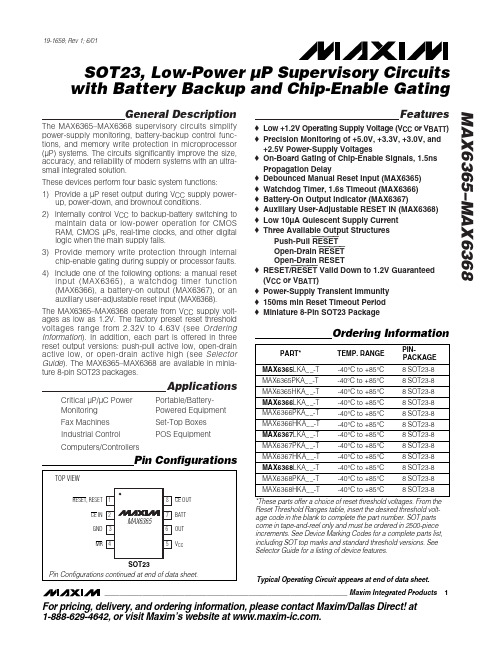
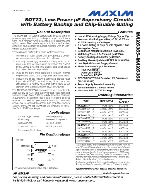
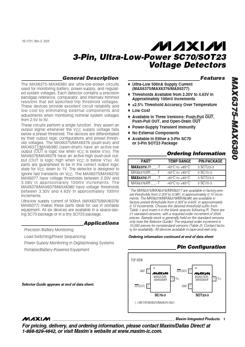
Pin Configurations
TOP VIEW
RESET, RESET 1 CE IN 2 GND 3 MR 4
MAX6365
8 CE OUT 7 BATT 6 OUT 5 VCC
Features
o Low +1.2V Operating Supply Voltage (VCC or VBATT) o Precision Monitoring of +5.0V, +3.3V, +3.0V, and
VCC, BATT, OUT.......................................................-0.3V to +6V RESET (open drain), RESET (open drain) ................-0.3V to +6V BATT ON, RESET (push-pull), RESET IN,
MAX6368LKA23-T中文资料

General DescriptionThe MAX6365–MAX6368 supervisory circuits simplify power-supply monitoring, battery-backup control func-tions, and memory write protection in microprocessor (µP) systems. The circuits significantly improve the size,accuracy, and reliability of modern systems with an ultra-small integrated solution.These devices perform four basic system functions:1) Provide a µP reset output during V CC supply power-up, power-down, and brownout conditions.2) Internally control V CC to backup-battery switching tomaintain data or low-power operation for CMOS RAM, CMOS µPs, real-time clocks, and other digital logic when the main supply fails.3) Provide memory write protection through internalchip-enable gating during supply or processor faults.4) Include one of the following options: a manual resetinput (MAX6365), a watchdog timer function (MAX6366), a battery-on output (MAX6367), or an auxiliary user-adjustable reset input (MAX6368).The MAX6365–MAX6368 operate from V CC supply volt-ages as low as 1.2V. The factory preset reset threshold voltages range from 2.32V to 4.63V (see Ordering Information ). In addition, each part is offered in three reset output versions: push-pull active low, open-drain active low, or open-drain active high (see Selector Guide ). The MAX6365–MAX6368 are available in minia-ture 8-pin SOT23 packages.ApplicationsCritical µP/µC Power Portable/Battery-Monitoring Powered Equipment Fax Machines Set-Top Boxes Industrial Control POS EquipmentComputers/ControllersFeatureso Low +1.2V Operating Supply Voltage (V CC or V BATT )o Precision Monitoring of +5.0V, +3.3V, +3.0V, and +2.5V Power-Supply Voltageso On-Board Gating of Chip-Enable Signals, 1.5ns Propagation Delayo Debounced Manual Reset Input (MAX6365)o Watchdog Timer, 1.6s Timeout (MAX6366)o Battery-On Output Indicator (MAX6367)o Auxiliary User-Adjustable RESET IN (MAX6368)o Low 10µA Quiescent Supply Current o Three Available Output StructuresPush-Pull RESET Open-Drain RESET Open-Drain RESETo RESET/RESET Valid Down to 1.2V Guaranteed (V CC or V BATT )o Power-Supply Transient Immunity o 150ms min Reset Timeout Period o Miniature 8-Pin SOT23 PackageMAX6365–MAX6368SOT23, Low-Power µP Supervisory Circuits with Battery Backup and Chip-Enable Gating________________________________________________________________Maxim Integrated Products1Pin Configurations19-1658; Rev 1; 6/01For pricing, delivery, and ordering information,please contact Maxim/Dallas Direct!at 1-888-629-4642, or visit Maxim’s website at .Ordering Information*These parts offer a choice of reset threshold voltages. From the Reset Threshold Ranges table, insert the desired threshold volt-age code in the blank to complete the part number. SOT parts come in tape-and-reel only and must be ordered in 2500-piece increments. See Device Marking Codes for a complete parts list,including SOT top marks and standard threshold versions. See Selector Guide for a listing of device features.Typical Operating Circuit appears at end of data sheet.M A X 6365–M A X 6368SOT23, Low-Power µP Supervisory Circuits with Battery Backup and Chip-Enable GatingABSOLUTE MAXIMUM RATINGSELECTRICAL CHARACTERISTICS(V = +2.4V to +5.5V, V = +3.0V, CE IN = V , reset not asserted, T = -40°C to +85°C. Typical values are at T = +25°C,Stresses beyond those listed under “Absolute Maximum Ratings” may cause permanent damage to the device. These are stress ratings only, and functional operation of the device at these or any other conditions beyond those indicated in the operational sections of the specifications is not implied. Exposure to absolute maximum rating conditions for extended periods may affect device reliability.Terminal Voltages (with respect to GND)V CC , BATT, OUT.......................................................-0.3V to +6V RESET (open drain), RESET (open drain)................-0.3V to +6V BATT ON, RESET (push-pull), RESET IN,WDI, CE IN, CE OUT...........................-0.3V to (V OUT + 0.3V)MR ..............................................................-0.3V to (V CC + 0.3V)Input CurrentV CC Peak ..............................................................................1A V CC Continuous.............................................................250mA BATT Peak.....................................................................250mA BATT Continuous.............................................................40mAGND...............................................................................75mA Output CurrentOUT...............................Short-Circuit Protected for up to 10s RESET, RESET , BATT ON, CE OUT...............................20mA Continuous Power Dissipation (T A = +70°C)8-Pin SOT23 (derate 8.75mW/°C above +70°C)........700mW Operating Temperature Range ...........................-40°C to +85°C Storage Temperature Range.............................-65°C to +150°C Junction Temperature .....................................................+150°C Lead Temperature (soldering, 10s).................................+300°CMAX6365–MAX6368SOT23, Low-Power µP Supervisory Circuits with Battery Backup and Chip-Enable Gating_______________________________________________________________________________________3ELECTRICAL CHARACTERISTICS (continued)(V CC = +2.4V to +5.5V, V BATT = +3.0V, CE IN = V CC , reset not asserted, T A = -40°C to +85°C. Typical values are at T A = +25°C,M A X 6365–M A X 6368SOT23, Low-Power µP Supervisory Circuits with Battery Backup and Chip-Enable Gating 4_______________________________________________________________________________________Typical Operating Characteristics(T A = +25°C, unless otherwise noted.)8109121115141316-400-2020406080SUPPLY CURRENTvs. TEMPERATURE (NO LOAD)TEMPERATURE (°C)S U P P L Y C U R R E N T (µA )0.20.60.40.81.01.2BATTERY SUPPLY CURRENT (BACKUP MODE) vs. TEMPERATURETEMPERATURE (°C)B A T T E R Y S U P P L YC U R R E N T (µA )-402040-200608021437658-40-2020406080BATT-TO-OUT ON-RESISTANCEvs. TEMPERATURETEMPERATURE (°C)B A T T -T O -O U T O N -R E S I S T A NC E (Ω)ELECTRICAL CHARACTERISTICS (continued)(V= +2.4V to +5.5V, V = +3.0V, CE IN = V , reset not asserted, T = -40°C to +85°C. Typical values are at T = +25°C,Note 2:V BATT can be 0 anytime, or V CC can go down to 0 if V BATT is active (except at startup).Note 3:RESET is pulled up to OUT. Specifications apply for OUT = V CC or OUT = BATT.Note 4:The chip-enable resistance is tested with V CC = V TH(MAX)and CE IN = V CC /2.MAX6365–MAX6368SOT23, Low-Power µP Supervisory Circuits with Battery Backup and Chip-Enable Gating_______________________________________________________________________________________5Typical Operating Characteristics (continued)(T A = +25°C, unless otherwise noted.)00.40.20.80.61.21.01.4-4020-20406080V CC TO OUT ON-RESISTANCEvs. TEMPERATURETEMPERATURE (°C)V C C T O O U T O N -R E S I S T A N C E (Ω)190195205200210RESET TIMEOUT PERIOD vs. TEMPERATUREM A X 6365/8-05TEMPERATURE (°C)R E S E T T I M E O U T P E R I O D (m s )-402040-206080301575604513512010590TEMPERATURE (°C)P R O P A G A T I O N D E L A Y (µs )-402040-206080V CC vs. TEMPERATURE2.03.02.55.04.54.03.5RESET THRESHOLD vs. TEMPERATURETEMPERATURE (°C)T H R E S H O L D (V )-402040-206080110010100010,000MAXIMUM TRANSIENT DURATION vs. RESET THRESHOLD OVERDRIVERESET THRESHOLD OVERDRIVE V TH - V CC (mV)M A X I M U M T R A N S I E N T D U R A T I O N (µs )40030035025020005015010003215498761000.5 1.0 1.5 2.0 2.5 3.0 3.5BATTERY SUPPLY CURRENT vs. SUPPLY VOLTAGEV CC (V)B A T T E R Y S U P P L YC U R R E N T (µA )M A X 6365–M A X 6368SOT23, Low-Power µP Supervisory Circuits with Battery Backup and Chip-Enable Gating 6_______________________________________________________________________________________1.2341.2351.236MAX6368RESET IN THRESHOLD vs. TEMPERATUREM A X 6365/8 -10TEMPERATURE (°C)V R T H (V )-402040-2060801.01.91.61.32.82.52.2MAX6368RESET IN TO RESET PROPAGATION DELAYvs. TEMPERATURETEMPERATURE (°C)P R O P A G A T I O N D E L A Y (µs )-402040-206080013245C LOAD (pF)P R O P A G A T I O N D E L A Y (n s )10050150200CHIP-ENABLE PROPAGATION DELAY vs. CE OUT LOAD CAPACITANCE515102025-40-2020406080TEMPERATURE (°C)C E I N T O C E O U T O N -R E S I S T A N C E (Ω)CE IN TO CE OUT ON-RESISTANCEvs. TEMPERATURE1.01.31.21.11.51.41.91.81.71.62.0-40-2020406080TEMPERATURE (°C)W A T C H D O G T I M E O U T P E R I O D (s )MAX6366WATCHDOG TIMEOUT PERIODvs. TEMPERATURETypical Operating Characteristics (continued)(T A = +25°C, unless otherwise noted.)MAX6365–MAX6368SOT23, Low-Power µP Supervisory Circuits with Battery Backup and Chip-Enable Gating_______________________________________________________________________________________7M A X 6365–M A X 6368SOT23, Low-Power µP Supervisory Circuits with Battery Backup and Chip-Enable Gating 8_______________________________________________________________________________________Detailed DescriptionThe Typical Operating Circuit shows a typical connec-tion for the MAX6365–MAX6368. OUT powers the static random-access memory (SRAM). If V CC is greater than the reset threshold (V TH ), or if V CC is lower than V TH but higher than V BATT , V CC is connected to OUT. If V CC is lower than V TH and V CC is less than V BATT ,BATT is connected to OUT. OUT supplies up to 150mA from V CC . In battery-backup mode, an internal MOSFET connects the backup battery to OUT. The on-resistance of the MOSFET is a function of backup-battery voltage and is shown in the BATT-to-OUT On-Resistance vs.Temperature graph in the T ypical Operating Char-acteristics .Chip-Enable Signal GatingThe MAX6365–MAX6368 provide internal gating of CE signals to prevent erroneous data from being written toCMOS RAM in the event of a power failure. During nor-mal operation, the CE gate is enabled and passes all CE transitions. When reset asserts, this path becomes disabled, preventing erroneous data from corrupting the CMOS RAM. All of these devices use a series trans-mission gate from CE IN to CE OUT. The 2ns propaga-tion delay from CE IN to CE OUT allows the devices to be used with most µPs and high-speed DSPs.During normal operation, CE IN is connected to CE OUT through a low on-resistance transmission gate.This is valid when reset is not asserted. If CE IN is high when reset is asserted, CE OUT remains high regard-less of any subsequent transitions on CE IN during the reset event.If CE IN is low when reset is asserted, CE OUT is held low for 12µs to allow completion of the read/write oper-ation (F igure 1). After the 12µs delay expires, the CEFunctional DiagramMAX6365–MAX6368SOT23, Low-Power µP Supervisory Circuits with Battery Backup and Chip-Enable Gating_______________________________________________________________________________________9OUT goes high and stays high regardless of any sub-sequent transitions on CE IN during the reset event.When CE OUT is disconnected from CE IN, CE OUT is actively pulled up to OUT.The propagation delay through the chip-enable circuit-ry depends on both the source impedance of the drive to CE IN and the capacitive loading at CE OUT. The chip-enable propagation delay is production tested from the 50% point of CE IN to the 50% point of CE OUT, using a 50Ωdriver and 50pF load capacitance.Minimize the capacitive load at CE OUT to minimize propagation delay, and use a low-output-impedance driver.Backup-Battery SwitchoverIn a brownout or power failure, it may be necessary to preserve the contents of the RAM. With a backup bat-tery installed at BATT, the MAX6365–MAX6368 auto-matically switch the RAM to backup power when V CC falls. The MAX6367 has a BATT ON output that goes high in battery-backup mode. These devices require two conditions before switching to battery-backup mode:1) V CC must be below the reset threshold.2) V CC must be below V BATT .Table 1 lists the status of the inputs and outputs in bat-tery-backup mode. The devices do not power up if theonly voltage source is on BATT. OUT only powers up from V CC at startup.Many µP-based products require manual reset capabili-ty, allowing the user or external logic circuitry to initiate a reset. For the MAX6365, a logic low on MR asserts reset.Reset remains asserted while MR is low and for a mini-mum of 150ms (t RP ) after it returns high. MR has an inter-nal 20k Ωpullup resistor to V CC . This input can be driven with TTL/CMOS logic levels or with open-drain/collector outputs. Connect a normally open momentary switch from MR to GND to create a manual reset function; exter-nal debounce circuitry is not required. If MR is driven from long cables or the device is used in a noisy environ-ment, connect a 0.1µF capacitor from MR to GND to pro-vide additional noise immunity.Figure 1. Reset and Chip-Enable TimingM A X 6365–M A X 6368SOT23, Low-Power µP Supervisory Circuits with Battery Backup and Chip-Enable Gating 10______________________________________________________________________________________Watchdog Input (MAX6366 Only)The watchdog monitors µP activity through the watch-dog input (WDI). If the µP becomes inactive, reset asserts. To use the watchdog function, connect WDI to a bus line or µP I/O line. A change of state (high to low,low to high, or a minimum 100ns pulse) resets the watchdog timer. If WDI remains high or low for longer than the watchdog timeout period (t WD ), the internal watchdog timer runs out and a reset pulse is triggered for the reset timeout period (t RP ). The internal watchdog timer clears whenever reset asserts or whenever WDI sees a rising or falling edge. If WDI remains in either a high or low state, a reset pulse asserts periodically after every t WD (F igure 2). Leave WDI unconnected to dis-able the watchdog function.BATT ON Indicator (MAX6367 Only)BATT ON is a push-pull output that drives high when in battery-backup mode. BATT ON typically sinks 3.2mA at 0.1V saturation voltage. In battery-backup mode, this terminal sources approximately 10µA from OUT. Use BATT ON to indicate battery-switchover status or to supply base drive to an external pass transistor for higher current applications (Figure 3).RESET IN Comparator (MAX6368 Only)RESET IN is compared to an internal 1.235V reference.If the voltage at RESET IN is less than 1.235V, reset asserts. Use the RESET IN comparator as an undervolt-age detector to signal a failing power supply or as a secondary power-supply reset monitor.To program the reset threshold (V RTH ) of the secondary power supply, use the following (see Typical Operating Circuit ):V RTH = V REF (R1 / R2 + 1)where V REF = 1.235V. To simplify the resistor selection,choose a value for R2 and calculate R1:R1 = R2 [(V RTH / V REF ) - 1]Since the input current at RESET IN is 25nA (max),large values (up to 1M Ω) can be used for R2 with no significant loss in accuracy. For example, in the Typical Operating Circuit , the MAX6368 monitors two supply voltages. To monitor the secondary 5V logic or analog supply with a 4.60V nominal programmed reset thresh-old, choose R2 = 100k Ω, and calculate R1 = 273k Ω.Reset OutputA µP ’s reset input starts the µP in a known state. The MAX6365–MAX6368 µP supervisory circuits assert a reset to prevent code-execution errors during power-up, power-down, and brownout conditions. RESET is guaranteed to be a logic low or logic high, depending on the device chosen (see Ordering Information ).RESET or RESET asserts when V CC is below the reset threshold and for at least 150ms (t RP ) after V CC rises above the reset threshold. RESET or RESET also asserts when MR is low (MAX6365) and when RESET IN is less than 1.235V (MAX6368). The MAX6366 watch-dog function will cause RESET (or RESET ) to assert in pulses following a watchdog timeout (Figure 2).Applications InformationOperation Withouta Backup Power SourceThe MAX6365–MAX6368 provide battery-backup func-tions. If a backup power source is not used, connect BATT to GND and OUT to V CC .Watchdog Software ConsiderationsOne way to help the watchdog timer monitor the soft-ware execution more closely is to set and reset the watchdog at different points in the program rather than pulsing the watchdog input periodically. F igure 4shows a flow diagram in which the I/O driving theFigure 2. MAX6366 Watchdog Timeout Period and Reset Active TimeMAX6365–MAX6368SOT23, Low-Power µP Supervisory Circuits with Battery Backup and Chip-Enable Gating______________________________________________________________________________________11watchdog is set low in the beginning of the program,set high at the beginning of every subroutine or loop,and set low again when the program returns to the beginning. If the program should hang in any subrou-tine, the problem would be quickly corrected.Replacing the Backup BatteryWhen V CC is above V TH , the backup power source can be removed without danger of triggering a reset pulse.The device does not enter battery-backup mode when V CC stays above the reset threshold voltage.Negative-Going V CC TransientsThese supervisors are relatively immune to short-dura-tion, negative-going V CC transients. Resetting the µP when V CC experiences only small glitches is usually not desirable.The T ypical Operating Characteristics section has a Maximum Transient Duration vs. Reset Threshold Overdrive graph for which reset is not asserted. The graph was produced using negative-going V CC pulses,starting at V CC and ending below the reset threshold by the magnitude indicated (reset threshold overdrive).The graph shows the maximum pulse width that a neg-ative-going V CC transient can typically have without triggering a reset pulse. As the amplitude of the tran-sient increases (i.e., goes further below the reset threshold), the maximum allowable pulse width decreases. Typically, a V CC transient that goes 100mV below the reset threshold and lasts for 30µs will not trig-ger a reset pulse.A 0.1µF bypass capacitor mounted close to the V CC pin provides additional transient immunity.M A X 6365–M A X 6368SOT23, Low-Power µP Supervisory Circuits with Battery Backup and Chip-Enable Gating 12______________________________________________________________________________________standard versions only. Contact factory for availability of nonstandard versions.MAX6365–MAX6368SOT23, Low-Power µP Supervisory Circuits with Battery Backup and Chip-Enable Gating______________________________________________________________________________________13Pin Configurations (continued)M A X 6365–M A X 6368SOT23, Low-Power µP Supervisory Circuits with Battery Backup and Chip-Enable Gating 14______________________________________________________________________________________Typical Operating CircuitChip InformationTRANSISTOR COUNT: 729PROCESS: CMOSSOT23, Low-Power µP Supervisory Circuitswith Battery Backup and Chip-Enable GatingMAX6365–MAX6368Maxim cannot assume responsibility for use of any circuitry other than circuitry entirely embodied in a Maxim product. No circuit patent licenses are implied. Maxim reserves the right to change the circuitry and specifications without notice at any time.Maxim Integrated Products, 120 San Gabriel Drive, Sunnyvale, CA 94086 408-737-7600 ____________________15©2001 Maxim Integrated Products Printed USAis a registered trademark of Maxim Integrated Products.Package Information。
AU6368中文资料

1D a t a B o o kAU6368USB2.0 Multiple SlotsFlash Memory Card Reader Technical Reference ManualP r o d u c t S p e c i f i c a t i o nOfficial ReleaseRevision 1.13WPublic Aug 2005Page 2 of 20AU6368 USB 2.0 Multiple Slots Flash Memory Card Reader V1.13WData sheet statusObjective specification This data sheet contains target or goal specifications for product development.Preliminary specification This data sheet contains preliminary data;supplementary data may be published later .Product specificationThis data sheet contains final product specifications.Revision HistoryDate Revision DescriptionMay 2005 1.11W/C31,C33, D31,D33 Removed the schematics.Please contact our sales if you need it. Aug 2005 1.12W/ C.D.E To modify “4.1 Pin Description” Pin- 12 Aug 20051.13W/ C.D.E1. To modify “5.2 Recommended OperatingConditions”2. Moved “3.0 Power Switch Feature” to “5.6Power Switch Feature”Page 3 of 20AU6368 USB 2.0 Multiple Slots Flash Memory Card Reader V1.13WCopyright NoticeCopyright 1997 - 2004 Alcor Micro Corp. All Rights Reserved.Trademark AcknowledgementsThe company and product names mentioned in this document may be the trademarks or registered trademarks of their manufacturers.DisclaimerAlcor Micro Corp. reserves the right to change this product without prior notice. Alcor Micro Corp. makes no warranty for the use of its products and bears noresponsibility for any error that appear in this document. Specifications are subject to change without prior notice.Contact Information:Web site: /TaiwanAlcor Micro Corp.4F , No 200 Kang Chien Rd., Nei Hu, Taipei, Taiwan, R.O.C. Phone: 886-2-8751-1984 Fax: 886-2-2659-7723Santa Clara Office Los Angeles Office 2901 Tasman Drive, Suite 206 9070 Rancho Park Court Santa Clara, CA 95054 Rancho Cucamonga, CA.91730USA USA Phone: (408) 845-9300 Phone: (909) 483-9900 Fax: (408) 845-9086 Fax: (909) 944-0464Table of Contents1 Introduction (6)1.1 Description (6)1.2 Features (6)2 Application Block Diagram (7)3 Pin Assignment (8)4 System Architecture and Reference Design (11)4.1 AU6368 Block Diagram (11)5 Electrical Characteristics (12)5.1 Absolute Maximum Ratings (12)5.2 Recommended Operating Conditions (12)5.3 General DC Characteristics (12)5.4 DC Electrical Characteristics for 5 volts operation (13)5.5 USB Transceiver Characteristics (14)5.6 Power Switch Feature (17)6 Mechanical Information (18)7 Abbreviations (19)Page 4 of 20 AU6368 USB 2.0 Multiple Slots Flash Memory Card Reader V1.13WOfficial Release_ PublicPage 5 of 20AU6368 USB 2.0 Multiple Slots Flash Memory Card Reader V1.13WOfficial Release_ PublicList of Figures2.1 Block Diagram ............................................................................................... 73.1 Pin Assignment Diagram ............................................................................. 84.1 AU6368 Block diagram .................................................................................115.1 Card Detect Power-on Timing .....................................................................176.1 Mechanical Information Diagram .. (18)List of Tables3.1 Pin Descriptions ........................................................................................ 95.1 Absolute Maximum Ratings ................................................................... 125.2 Recommended Operating Conditions .................................................. 125.3 General DC Characteristics .................................................................... 125.4 DC Electrical Characteristics of 3.3V I/O Cells ........................... 135.5 Recommended Operation Conditions .................................................. 145.6 Static characteristic :Digital in ........................................................... 145.7 Static characteristic :Analog I/O pins (DP/DM )..............................155.8 Dynamic characteristic :Analog I/O pins (DP/DM ) (16)Page 6 of 20AU6368 USB 2.0 Multiple Slots Flash Memory Card Reader V1.13WOfficial Release_ Public1.0 Introduction1.1 DescriptionThe AU6368 is an integrated single chip memory card reader controller specially designed for notebook, hand-held and other PC peripheral devices, which require fewer components for small PCB area. It supports a widely used flash memory card such as CF , MD, SMC, xD Picture Card, MS, MS Pro, MS Duo, SD and MMC. It can be used as removable storage disks in enormous data exchange applications between PC and PC or PC and various consumer electronic appliances.The AU6368 reads digital content saved on memory card that user captured with the portable device such as notebook, digital camera, MP3 player , PDA and mobile phone… etc. In addition, AU6368 allows user to transfer information such as data, graphics, texts or digital images from one electronic device to another quickly and easily. Furthermore, AU6368 integrates power switch function; manufacturers can use fewer components in their product design.With AU6368, user’s experience will be also further enhanced by the Plug-and-Play nature built into latest operation systems such as Windows 2000/XP and Mac OS X.1.2 FeaturesSupport USB v2.0 specification and USB Device Class Definition for MassStorage, Bulk-Transport v1.0Support CF/MD, SD/MMC, MS/MS PRO/MS ROM/MS Duo AND xD/SMCspecificationWork with default driver from Windows ME, Windows XP , and Mac OS X.Windows 98, Windows 2000 are supported by vendor AP (The AP included both win98 and 2000 driver) from Alcor .Ping-pong FIFO implementation for concurrent bus operation Support multiple sectors transfer optimize performance Support slot-to-slot read/write operation.Support auto-detecting slot with card inserted on Win 2000 without driver . Capable of handing 4 sets of built-in PID, VID and strings to minimizeinventory control and improve lead production lead-time. Support LED for bus activity indication.Each slot can be enables/disabled by 5 independent pins to fit all thedifferent card readers’ combination requirement. Runs at 30MHz, built-in 480 MHz PLL Built-in 3.3V to 2.5V regulatorPage 7 of 20AU6368 USB 2.0 Multiple Slots Flash Memory Card Reader V1.13WOfficial Release_ Public2.0 Application Block DiagramFollowing is the application diagram of a typical card reader product with AU6368. By connecting the card reader to a desktop or notebook PC through USB bus,AU6368 is implemented as a bus-powered, high speed USB card reader , which can be used as a bridge for data transfer between Desktop PC and Notebook PC.2.1 Block DiagramUSB 9-in-1 Flash MemoryCard ReaderSMC/SD/MMCPage 8 of 20AU6368 USB 2.0 Multiple Slots Flash Memory Card Reader V1.13WOfficial Release_ Public3.0 Pin AssignmentThe AU6368 is packed in 80pin-LQFP-form factor . The following figure shows signal name for each pin and the table in the following page describes each pin in detail.Figure 3.1 Pin Assignment DiagramGPI0SDDATA3SDDATA2SDDATA1SDDATA0SDWP SDCDN SDCLK SDCMD PWRLED X_IN X_OUTRREF AVSS PVDD GPON7RPU AVDDDP DM VDD25VPVSSVSSHVDD33VDDHCF_V33MS_VCCSD_VCCXD_V33MSDATA0MSCLKMSDATA2MSDATA3MSDATA1SMDATA6SMDATA5MSINSMSBSSMDATA7SMDATA3SMDATA1SMDATA0SMDATA2GND VDD XDCDN XDCEN XDWPN SMCEN SMWPN SMRBN SMWRN SMCDN SMALE SMRDN RSTN CFD7SMCLE CFD5CFD3CFD2CFD4CFD0CFD1CFWTNCFOENCFWEN CFAD0CFAD1RFU0CUSELCFCDNCFRDNCFWRNCFAD3CFAD2CFAD9SMDATA4CFD6GPI1Page 9 of 20AU6368 USB 2.0 Multiple Slots Flash Memory Card Reader V1.13WOfficial Release_ PublicTable 3.1 Pin DescriptionsPin #Pin NameI/ODescription1 GPI0I Slot Mode Select(GPI1, GPI0) = (0,0) : Reserved (GPI1, GPI0) = (0,1) : 2 Luns(GPI1, GPI0) = (1,0) : 4.5 Luns (GPI1, GPI0) = (1,1) : 1 Lun2 SDDATA3 I/O SD Data3 3 SDDATA2 I/O SD Data24 SDDATA1 I/O SD Data15 SDDATA0 I/O SD Data06 SDWP I SD Write Protect7 SDCDN I SD Card Detect8 SDCLK O SD CLK9 SDCMD I/O SD CMD 10 PWRLED O Power LED; (Normal:"0"; Suspend"1") 11 GPON7 O Card insert LED; (Card inserted:"0"; 12 RPU I Connected with an 1.5k pull up resistor to 3.3 VDD 13 AVDD I Analog Power 3.3V 14 DP I/O USB DP 15 DM I/O USB DM16 AVSS PWR Analog Ground 17 RREF I Connected an 1k resistor to GND for impedance match 18 PVDD I OSC Power 3.3V 19 X_IN I 12 MHz crystal input. 20 X_OUT O 12 MHz crystal output. 21 PVSS PWR OSC Ground 22 VDD25V O Core Power 2.5V 23 VDDH I IO Power 3.3V 24 VSSH PWR IO Ground 25 VDD33 I Switch Power 3.3V 26 CF_V33 O CF Card Power 27 XD_V33 O SMC and XD share XD_V33 Power 28 MS_VCC O MS Card Power 29 SD_VCC O SD Card Power 30 MSDATA3 I/O MS Data3 31 MSDATA2 I/O MS Data2 32 MSDATA1 I/O MS Data1 33 MSDATA0 I/O MS Data0 34 MSCLK O MS CLK 35 MSBS O MS BS 36 MSINS I MS INS 37 SMDATA7 I/O SMDATA7 38 SMDATA6 I/O SMDATA6 39 SMDATA5 I/O SMDATA5 40 SMDATA4 I/O SMDATA4 41 SMDATA3I/O SMDATA3Page 10 of 20AU6368 USB 2.0 Multiple Slots Flash Memory Card Reader V1.13WOfficial Release_ Public42 SMDATA2 I/O SMDATA2 43 SMDATA1 I/O SMDATA1 44 SMDATA0 I/O SMDATA045 VDD I Core power 2.5V 46 GND PWR Core Ground 47 XDWPN O XD WP 48 XDCDN I XD CD 49 XDCEN O XD CE 50 SMWPN I SMC WP 51 SMCEN O SMC CE 52 SMCDN I SMC CD53 SMRBN I SMC read/busy. External pull up with 470K to 3.3V . 54 SMWRN O SM WRN 55 SMRDN O SMRDN 56 SMALE O SM ALE 57 SMCLE O SM CLE58 RSTN I Chip Reset (Reset:"0"; Normal:"1"), pull up with RC 59 CFD7 I/O CF Data7 60 CFD6 I/O CF Data6 61 CFD5 I/O CF Data5 62 CFD4 I/O CF Data4 63 CFD3 I/O CF Data3 64 CFD2 I/O CF Data2 65 CFD1 I/O CF Data1 66 CFD0 I/O CF Data0 67 CFWEN O CF WEN 68 CFWTN I CF WAITN 69 CFOEN O CF OE70 CFWRN O CF IOWRN 71 CFRDN O CF IORDN 72 CFAD9 O CF Addr9 73 CFAD3 O CF Addr3 74 CFAD2 O CF Addr2 75 CFAD1 O CF Addr1 76 CFAD0 O CF Addr0 77 CFCDN I CF CD78 RFU0 I Always pull Low 79 CUSEL I Always pull High 80GPI1ISlot Mode Select(GPI1, GPI0) = (0,0) : Reserved(GPI1, GPI0) = (0,1) : 2 Luns (GPI1, GPI0) = (1,0) : 4.5 Luns (GPI1, GPI0) = (1,1) : 1 LunPage 11 of 204.0 System Architecture andReference Design4.1 AU6368 Block DiagramFigure 4.1 AU6368 Block DiagramCF MD SM SD MMC xD MSUSB Upstream PortPage 12 of 205.0 Electrical Characteristics5.1 Absolute Maximum RatingsTable 5.1 Absolute Maximum RatingsSYMBOLPARAMETER RATING UNITS V CC Power Supply -0.3 to V CC +0.3 V V IN Input Voltage -0.3 to 3.3 V V OUT Output Voltage -0.3 to V CC +0.3 VT STG Storage Temperature-40 to 150OC5.2 Recommended Operating ConditionsTable 5.2 Recommended Operating ConditionsSYMBOLPARAMETER MIN TYP MAX UNITS V CC Power Supply 3.0 3.3 3.6 V V IN Input Voltage 0 3.3 5.2 VT OPR Operating Temperature25125OC5.3 Leakage Current and CapacitanceTable 5.3 General DC CharacteristicsSYMBOLPARAMETER CONDITIONS MIN TYP MAX UNITS I IN Input current no pull-up or pull-down-10 ±1 10 µA I OZ Tri-state leakage current-10 ±1 10 µA C IN Input capacitance Pad Limit 2.8 ρF C OUT Output capacitance Pad Limit 2.8 ρF C BID Bi-directional buffercapacitancePad Limit2.8ρFPage 13 of 205.4 DC Electrical Characteristics of 3.3V I/O CellsTable 5.4 DC Electrical Characteristics of 3.3V I/O CellsLimitsSYMBOL PARAMETER CONDITIONSMIN TYP MAX UNIT V CC Power supply 3.3V I/O 3.0 3.3 3.6 V V il Input low voltage0.8 V V ih Input high voltage LVTTL2.0 V V ol Output low voltage ∣I ol ∣=2~16mA 0.4 V V oh Output high voltage ∣I oh ∣=2~16mA 2.4 V R pu Input pull-up resistancePU=high, PD=low40 75 190 K Ω R pd Input pull-down resistance PU=low, PD=high 40 75 190 K Ω I in Input leakage current V in = V CC or 0-10 ±1 10 μA I oz Tri-state output leakagecurrent-10±110μAPage 14 of 205.5 USB Transceiver CharacteristicsTable 5.5 Electrical characteristicsSymbol Parameter ConditionsMin. Typ. Max. Unit AVCC Analog supply current 3.0 3.3 3.6 V VCC Digital supply current2.252.52.75VI CCOperating supply currentHigh speed operatingat 480 MHz 73 mAI CC(susp) Suspend supply currentIn suspend mode, current with 1.5k Ωpull-up resistor on pin RPU disconnected 120 µATable 5.6 Static characteristic :Digital pinSymbolParameterConditions Min.Typ.Max.UnitInput levelsV IL Low-level input voltage 0.8 V V IH High-level input voltage2.0VOutput levelsV OL Low-level output voltage0.2 VV OH High-level output voltage VCC-0.2 VAVCC=3.0V~3.6V ;VCC=2.25V~2.75V ;Temp=0℃~115℃Table 5.7 Static characteristic:Analog I/O pins(DP/DM)Symbol Parameter Conditions Min. Typ. Max. UnitUSB2.0 Transceiver(HS)Input Levels(differential receiver)V HSDIFF High speed differentialinput sensitivity∣V I(DP)-V I(DM)∣measured at theconnection asapplication circuit300 mVV HSCM High speed data signalingcommon mode voltagerange-50 500mVSquelch detected 100 mVV HSSQ High speed squelchdetection threshold No squelch detected 150 mVDisconnectiondetected 625 mV V HSDSC High speed disconnectiondetection threshold Disconnection notdetected 525mVOutput LevelsV HSOI High speed idle leveloutputvoltage(differential)-10 10mVV HSOL High speed low leveloutputvoltage(differential)-10 10mVV HSOH High speed high leveloutputvoltage(differential)-360 400mVV CHIRPJ Chirp-J output voltage(differential)700 1100mVV CHIRPK Chirp-K output voltage(differential)-900 -500 mVResistanceEquivalent resistanceused as internal chiponly3 6 9R DRV Driver output impedanceOverall resistance including externalresistor 40.5 45 49.5ΩTerminationV TERM Termination voltage forpull-up resistor on pinRPU3.0 3.6V USB1.1 Transceiver(FS/LS)Input Levels(differential receiver)V DI Differential inputsensitivity ∣V I(DP)-V I(DM)∣0.2 VV CM Differential commonmode voltage 0.8 2.5V Input Levels(single-ended receivers)Page 15 of 20Page 16 of 20V SESingle ended receiverthreshold0.8 2.0 VOutput levelsV OL Low-level output voltage0.3 VV OH High-level output voltage 2.8 3.6 VAVCC=3.0V~3.6V ;VCC=2.25V~2.75V ;Temp=0℃~115℃Table 5.8 Dynamic characteristic :Analog I/O pins (DP/DM )SymbolParameterConditionsMin. Typ. Max. UnitDriver Characteristics High-Speed Modet HSR High-speed differentialrise time500 ps t HSFHigh-speed differentialfall time500 psFull-Speed Modet FR Rise timeCL=50pF ;10 to 90﹪of ∣V OH -V OL ∣; 4 20 ns t FF Fall timeCL=50pF ;90 to 10﹪of ∣V OH -V OL ∣; 4 20 ns t FRMA Differential rise/fall timematching (t FR / t FF )Excluding the firsttransition from idlemode90 110 % V CRS Output signal crossovervoltageExcluding the firsttransition from idlemode1.32.0 VLow-Speed Modet LR Rise time CL=200pF-600pF ;10 to 90﹪of∣V OH -V OL ∣; 75 300 nst LF Fall time CL=200pF-600pF ;90 to 10﹪of∣V OH -V OL ∣; 75 300 nst LRMA Differential rise/fall timematching (t LR / t LF )Excluding the firsttransition from idlemode80 125 % V CRS Output signal crossovervoltageExcluding the firsttransition from idlemode 1.3 2.0 VV OH High-level output voltage 2.8 3.6 VPage 17 of 205.6 Power Switch FeatureAU6368 integrates a 3.3V to 2.5V voltage regulator and power switch to replace all MOS chips for flash card power supply.Card Power Output Current RangeFor MS/SDMAX: 100mA For XD/SMCMAX: 70mA For CFMAX: 250mACard power output voltage rangeMS/XD/SD/SMC/CF: 3.3V ±0.3VAU6368 will turn off all of Card Power in suspend modeFigure 5.1 Card Detect Power-on Timing3.3V+/- 0.3V1ms to 10ms ( Depend Load Capacitor )CARD_POWERCARD_DETECT100ms + System Polling timingPage 18 of 206.0 Mechanical InformationFigure 6.1 Mechanical Information DiagramPage 19 of 207.0 AbbreviationsThis chapter lists and defines terms and abbreviations used throughout this specification.SIE Serial Interface Engine CF Compact Flash MD Micro Drive SMC SmartMedia Card MS Memory Stick SD Secure Digital MMC Multimedia CardUTMI USB Transceiver Macrocell InterfacePage 20 of 20【MEMO 】About Alcor Micro, CorpAlcor Micro, Corp. designs, develops and markets highly integrated and advanced peripheral semiconductor, and software driver solutions for the personal computer and consumer electronics markets worldwide. We specialize in USB solutions and focus on emerging technology such as USB and IEEE 1394. The company offers a range of semiconductors including controllers for USB hub, integratedkeyboard/USB hub and USB Flash memory card reader…etc. Alcor Micro, Corp. is based in Taipei, Taiwan, with sales offices in Taipei, Japan, Korea and California. Alcor Micro is distinguished by its ability to provide innovative solutions forspec-driven products. Innovations like single chip solutions for traditional multiple chip products and on-board voltage regulators enable the company to provide cost-efficiency solutions for the computer peripheral device OEM customers worldwide.。
MAX6368PKA46+T中文资料
VCC Peak ..............................................................................1A VCC Continuous .............................................................250mA BATT Peak .....................................................................250mA
MAX6368HKA_ _-T
-40°C to +85°C
8 SOT23-8
*These parts offer a choice of reset threshold voltages. From the Reset Threshold Ranges table, insert the desired threshold voltage code in the blank to complete the part number. SOT parts come in tape-and-reel only and must be ordered in 2500-piece increments. See Device Marking Codes for a complete parts list, including SOT top marks and standard threshold versions. See Selector Guide for a listing of device features.
MAX6378XR36-T中文资料
General DescriptionThe MAX6375–MAX6380 are ultra-low-power circuits used for monitoring battery, power-supply, and regulat-ed system voltages. Each detector contains a precision bandgap reference, comparator, and internally trimmed resistors that set specified trip threshold voltages.These devices provide excellent circuit reliability and low cost by eliminating external components and adjustments when monitoring nominal system voltages from 2.5V to 5V.These circuits perform a single function: they assert an output signal whenever the V CC supply voltage falls below a preset threshold. The devices are differentiated by their output logic configurations and preset thresh-old voltages. The MAX6375/MAX6378 (push-pull) and MAX6377/MAX6380 (open-drain) have an active-low output (OUT is logic low when V CC is below V TH ). The MAX6376/MAX6379 have an active-high push-pull out-put (OUT is logic high when V CC is below V TH ). All parts are guaranteed to be in the correct output logic state for V CC down to 1V. The detector is designed to ignore fast transients on V CC . The MAX6375/MAX6376/MAX6377 have voltage thresholds between 2.20V and 3.08V in approximately 100mV increments. The MAX6378/MAX6379/MAX6380 have voltage thresholds between 3.30V and 4.63V in approximately 100mV increments.Ultra-low supply current of 500nA (MAX6375/MAX6376/MAX6377) makes these parts ideal for use in portable equipment. All six devices are available in a space-sav-ing SC70 package or in a tiny SOT23 package.ApplicationsPrecision Battery Monitoring Load Switching/Power SequencingPower-Supply Monitoring in Digital/Analog Systems Portable/Battery-Powered EquipmentFeatureso Ultra-Low 500nA Supply Current (MAX6375/MAX6376/MAX6377)o Thresholds Available from 2.20V to 4.63V in Approximately 100mV Incrementso ±2.5% Threshold Accuracy Over Temperature o Low Costo Available in Three Versions: Push-Pull OUT ,Push-Pull OUT, and Open-Drain OUT o Power-Supply Transient Immunity o No External Components o Available in Either a 3-Pin SC70 or 3-Pin SOT23 PackageMAX6375–MAX63803-Pin, Ultra-Low-Power SC70/SOT23Voltage Detectors________________________________________________________________Maxim Integrated Products 1Pin Configuration19-1721; Rev 2; 2/03*The MAX6375/MAX6376/MAX6377 are available in factory-pre-set thresholds from 2.20V to 3.08V, in approximately 0.1V incre-ments. The MAX6378/MAX6379/MAX6380 are available infactory-preset thresholds from 3.30V to 4.63V, in approximately 0.1V increments. Choose the desired threshold suffix fromTable 1 and insert it in the blank spaces following R.There are 21 standard versions, with a required order increment of 2500pieces. Sample stock is generally held on the standard versions only (see the Selector Guide). The required order increment is 10,000 pieces for nonstandard versions (Table 2). Contact facto-ry for availability. All devices available in tape-and-reel only.Selector Guide appears at end of data sheet.For pricing, delivery, and ordering information,please contact Maxim/Dallas Direct!at 1-888-629-4642, or visit Maxim’s website at .Ordering information continued at end of data sheetM A X 6375–M A X 63803-Pin, Ultra-Low-Power SC70/SOT23Voltage Detectors 2_______________________________________________________________________________________ABSOLUTE MAXIMUM RATINGSELECTRICAL CHARACTERISTICS(V CC = full range, T A = -40°C to +85°C, unless otherwise noted. Typical values are at T A = +25°C and V CC = 3V.) (Note 1)Stresses beyond those listed under “Absolute Maximum Ratings” may cause permanent damage to the device. These are stress ratings only, and functional operation of the device at these or any other conditions beyond those indicated in the operational sections of the specifications is not implied. Exposure to absolute maximum rating conditions for extended periods may affect device reliability.Terminal Voltage (with respect to GND)V CC ...........................................................................-0.3V to +6V OUT, OUT (push-pull)................................-0.3V to (V CC + 0.3V)OUT (open-drain).....................................................-0.3V to +6V Input Current (V CC ).............................................................20mA Output Current (OUT, OUT )................................................20mAContinuous Power Dissipation (T A = +70°C)3-Pin SC70 (derate 2.17mW/°C above +70°C)...........174mW 3-Pin SOT23 (derate 4mW/°C above +70°C)..............320mW Operating Temperature Range ...........................-40°C to +85°C Storage Temperature Range.............................-65°C to +150°C Junction Temperature......................................................+150°C Lead Temperature (soldering, 10s).................................+300°CNote 1:Production tested at +25°C only. Overtemperature limits are guaranteed by design, not production tested.MAX6375–MAX63803-Pin, Ultra-Low-Power SC70/SOT23Voltage Detectors__________________________________________Typical Operating Characteristics(V CC = 5V, T A = +25°C, unless otherwise noted.)00.30.20.10.40.50.60.70.80.91.0-40-2020406080SUPPLY CURRENT vs. TEMPERATURETEMPERATURE (°C)S U P P L Y C U R R E N T (µA )050100150200-40-2020406080PROPAGATION DELAY (FALLING)vs. TEMPERATURETEMPERATURE (°C)P R O P A G A T I O N D E L A Y (µs )040208060120100140-4020-20406080PROPAGATION DELAY (RISING)vs. TEMPERATURETEMPERATURE (°C)P R O P A G A T I O N D E L A Y (µs )50011001000MAXIMUM TRANSIENT DURATION vs. THRESHOLD OVERDRIVE100300400200THRESHOLD OVERDRIVEV TH - V CC (mV)M A X I M U M T R A N S I E N T D U R A T I O N (µs )10Pin DescriptionM A X 6375–M A X 63803-Pin, Ultra-Low-Power SC70/SOT23Voltage Detectors____________Applications InformationInterfacing to Different Logic Voltage ComponentsThe MAX6377/MAX6380 have an active-low, open-drain output. This output structure sinks current when OUT is asserted. Connect a pullup resistor from OUT to any supply voltage up to 5.50V (Figure 1). Select a resistor value large enough to allow a valid logic low (see Electrical Characteristics ), and small enough to register a logic high while supplying all input current and leakage paths connected to the OUT line.Negative-Going V CC TransientsThese devices are relatively immune to short-duration,negative-going V CC transients (glitches). The Typical Operating Characteristics show the Maximum Transient Duration vs. Threshold Overdrive graph, for which out-put pulses are not generated. The graph shows the maximum pulse width that a negative-going V CC tran-sient may typically have before the devices issue out-put signals. As the amplitude of the transient increases,the maximum-allowable pulse width decreases.Figure 1. Interfacing to Different Logic Voltage ComponentsTable 1. Factory-Trimmed Reset Thresholds ‡3-Pin, Ultra-Low-Power SC70/SOT23Voltage Detectors_______________________________________________________________________________________5Table 2. Device Marking Codes and Minimum Order IncrementsMAX6375–MAX6380M A X 6375–M A X 63803-Pin, Ultra-Low-Power SC70/SOT23Voltage Detectors 6___________________Chip InformationTRANSISTOR COUNT: 419Selector Guide**S ample stock is generally held on all standard versions.Contact factory for availability of nonstandard versions.Maxim cannot assume responsibility for use of any circuitry other than circuitry entirely embodied in a Maxim product. No circuit patent licenses are implied. Maxim reserves the right to change the circuitry and specifications without notice at any time.Maxim Integrated Products, 120 San Gabriel Drive, Sunnyvale, CA 94086 408-737-7600_____________________7©2003 Maxim Integrated ProductsPrinted USAis a registered trademark of Maxim Integrated Products.3-Pin, Ultra-Low-Power SC70/SOT23Voltage DetectorsMAX6375–MAX6380Package Information(The package drawing(s) in this data sheet may not reflect the most current specifications. For the latest package outline information,go to /packages .)。
MAX3087ESA中文资料
375
256
MAX3084
Full
0.5
Yes
No
No
375
256
MAX3085
Half
0.5
Yes
Yes
Yes
375
256
MAX3086
Full
10
No
Yes
Yes
375
256
MAX3087
Full
10
No
No
No
375
256
MAX3088
Half
10
No
Yes
Yes
375
256
MAX3089 Selectable Selectable Selectable
These transceivers typically draw 375µA of supply current when unloaded, or when fully loaded with the drivers disabled.
All devices have a 1/8-unit-load receiver input impedance that allows up to 256 transceivers on the bus. The MAX3082/MAX3085/MAX3088 are intended for halfduplex communications, while the MAX3080/MAX3081/ MAX3083/MAX3084/MAX3086/MAX3087 are intended for full-duplex communications. The MAX3089 is selectable between half-duplex and full-duplex operation. It also features independently programmable receiver and transmitter output phase via separate pins.
MX636JH中文资料

General DescriptionThe MX536A and MX636 are true RMS-to-DC convert-ers. They feature low power and are designed to accept low-level input signals from 0 to 7V RMS for the MX536A and 0 to 200mV RMS for the MX636. Both devices accept complex input waveforms containing AC and DC com-ponents. They can be operated from either a single sup-ply or dual supplies. Both devices draw less than 1mA of quiescent supply current, making them ideal for bat-tery-powered applications.Input and output offset, positive and negative waveform symmetry (DC reversal), and full-scale accuracy are laser trimmed, so that no external trims are required to achieve full rated accuracy.________________________ApplicationsDigital MultimetersBattery-Powered Instruments Panel Meters Process Control____________________________Featureso True RMS-to-DC Conversiono Computes RMS of AC and DC Signals o Wide Response:2MHz Bandwidth for V RMS > 1V (MX536A)1MHz Bandwidth for V RMS > 100mV (MX636)o Auxiliary dB Output:60dB Range (MX536A)50dB Range (MX636)o Single- or Dual-Supply Operation o Low Power: 1.2mA typ (MX536A)800µA typ (MX636)MX536A/MX636True RMS-to-DC Converters________________________________________________________________Maxim Integrated Products1Pin Configurations_________Typical Operating Circuits19-0824; Rev 2; 3/96Ordering Information continued at end of data sheet.*Maxim reserves the right to ship ceramic packages in lieu of CERDIP packages.** Dice are specified at T A = +25°C.For free samples & the latest literature: , or phone 1-800-998-8800.For small orders, phone 408-737-7600 ext. 3468.M X 536A /M X 636True RMS-to-DC Converters 2_______________________________________________________________________________________ABSOLUTE MAXIMUM RATINGSELECTRICAL CHARACTERISTICS—MX536A(T A = +25°C, +V S = +15V, -V S = -15V, unless otherwise noted.)Stresses beyond those listed under “Absolute Maximum Ratings” may cause permanent damage to the device. These are stress ratings only, and functional operation of the device at these or any other conditions beyond those indicated in the operational sections of the specifications is not implied. Exposure to absolute maximum rating conditions for extended periods may affect device reliability.Supply Voltage:Dual Supplies (MX536A)............................±18V(MX636).............................±12VSingle Supply (MX536A)...........................+36V(MX636).............................+24VInput Voltage (MX536A).......................................................±25V(MX636).........................................................±12VPower Dissipation (Package)Plastic DIP (derate 12mW/°C above +75°C)...............450mW Small Outline (derate 10mW/°C above +75°C)............400mW Ceramic (derate 10mW/°C above +75°C)...................500mW TO-100 metal can (derate 7mW/°C above +75°C)......450mWOutput Short-Circuit Duration........................................Indefinite Operating Temperature RangesCommercial (J, K)...............................................0°C to +70°C Military (S)......................................................-55°C to +125°C Storage Temperature Range.............................-55°C to +150°C Lead Temperature (soldering, 10sec)................................300°CMX536A/MX636True RMS-to-DC Converters_______________________________________________________________________________________3ELECTRICAL CHARACTERISTICS—MX536A (continued)(T A = +25°C, +V S = +15V, -V S = -15V, unless otherwise noted.)M X 536A /M X 636True RMS-to-DC Converters 4_______________________________________________________________________________________ELECTRICAL CHARACTERISTICS—MX536A (continued)(T A = +25°C, +V S = +15V, -V S = -15V, unless otherwise noted.)ELECTRICAL CHARACTERISTICS—MX636(T A = +25°C, +V S = +3V, -V S = -5V, unless otherwise noted.)MX536A/MX636True RMS-to-DC Converters_______________________________________________________________________________________5ELECTRICAL CHARACTERISTICS—MX636 (continued)(T= +25°C, +V = +3V, -V = -5V, unless otherwise noted.)M X 536A /M X 636_______________Detailed DescriptionThe MX536A/MX636 uses an implicit method of RMS computation that overcomes the dynamic range as well as other limitations inherent in a straightforward compu-tation of the RMS. The actual computation performed by the MX536A/MX636 follows the equation:V RMS = Avg. [V IN 2/V RMS ]The input voltage, V IN , applied to the MX536A/MX636 is processed by an absolute-value/voltage to current con-verter that produces a unipolar current I 1(Figure 1).This current drives one input of a squarer/divider that produces a current I 4that has a transfer function:I 4= I 12I 3The current I 4drives the internal current mirror through a lowpass filter formed by R1 and an external capaci-tor, C AV . As long as the time constant of this filter is greater than the longest period of the input signal, I 4is averaged. The current mirror returns a current, I 3, to the square/divider to complete the circuit. The current I 4is then a function of the average of (I 12/I 4), which is equal to I 1RMS .The current mirror also produces a 2 · I 4output current,I OUT , that can be used directly or converted to a volt-age using resistor R2 and the internal buffer to provide a low-impedance voltage output. The transfer function for the MX536A/MX636 is:V OUT = 2 · R2 · I RMS = V INThe dB output is obtained by the voltage at the emitter of Q3, which is proportional to the -log V IN . The emitter follower Q5 buffers and level shifts this voltage so that the dB output is zero when the externally set emitter current for Q5 approximates I 3.Standard Connection(Figure 2)The standard RMS connection requires only one exter-nal component, C AV . In this configuration the MX536A/MX636 measures the RMS of the AC and DC levels present at the input, but shows an error for low-frequency inputs as a function of the C AV filter capaci-tor. Figure 3 gives practical values of C AV for various values of averaging error over frequency for the stan-dard RMS connections (no post filtering). If a 3µF capacitor is chosen, the additional error at 100Hz will be 1%. If the DC error can be rejected, a capacitor should be connected in series with the input, as would typically be the case in single-supply operation.The input and output signal ranges are a function of the supply voltages. Refer to the electrical characteristics for guaranteed performance. The buffer amplifier can be used either for lowering the output impedance of the cir-cuit, or for other applications such as buffering high-impedance input signals. The MX536A/MX636 can be used in current output mode by disconnecting the inter-nal load resistor, R L , from ground. The current output is available at pin 8 (pin 10 on the “H” package) with a nominal scale of 40µA/V RMS input for the MX536A and 100µA/V RMS input for the MX636. The output is positive.True RMS-to-DC Converters 6_______________________________________________________________________________________ELECTRICAL CHARACTERISTICS—MX636 (continued)(T= +25°C, +V = +3V, -V = -5V, unless otherwise noted.)Note 1:Accuracy is specified for 0 to 7V RMS , DC or 1kHz sine-wave input with the MX536A connected as in Figure 2.Note 2:Error vs. crest factor is specified as an additional error for 1V RMS rectangular pulse stream, pulse width = 200µs.Note 3:Input voltages are expressed in volts RMS, and error as % of reading.Note 4:With 2k Ωexternal pull-down resistor.Note 5:Accuracy is specified for 0 to 200mV, DC or 1kHz sine-wave input. Accuracy is degraded at higher RMS signal levels.Note 6:Measured at pin 8 of DIP and SO (I OUT ), with pin 9 tied to COMMON.Note 7:Error vs. crest factor is specified as an additional error for 200mV RMS rectangular pulse input, pulse width = 200µs.Note 8:Input voltages are expressed in volts RMS.Note 9:With 10k Ωexternal pull-down resistor from pin 6 (BUF OUT) to -V S .Note 10:With BUF input tied to COMMON.MX536A/MX636True RMS-to-DC Converters_______________________________________________________________________________________7Figure 1. MX536A Simplified SchematicFigure 2. MX536A/MX636 Standard RMS ConnectionM X 536A /M X 636High-Accuracy AdjustmentsThe accuracy of the MX536A/MX636 can be improved by the addition of external trims as shown in Figure 4.R4 trims the offset. The input should be grounded and R4 adjusted to give zero volts output from pin 6. R1 is trimmed to give the correct value for either a calibrated DC input or a calibrated AC signal. For example: 200mV DC input should give 200mV DC output; a ±200mV peak-to-peak sine-wave should give 141mV DC output.Single-Supply OperationBoth the MX536A and the MX636 can be used with a single supply down to +5V (Figure 5). The major limita-tion of this connection is that only AC signals can be measured, since the differential input stage must be biased off ground for proper operation. The load resis-tor is necessary to provide output sink current. The input signal is coupled through C2 and the value cho-sen so that the desired low-frequency break point is obtained with the input resistance of 16.7k Ωfor the MX536A and 6.7k Ωfor the MX636.Figure 5 shows how to bias pin 10 within the range of the supply voltage (pin 2 on “H” packages). It is critical that no extraneous signals are coupled into this pin. A capacitor connected between pin 10 and ground is recommended. The common pin requires less than 5µA of input current, and if the current flowing through resis-tors R1 and R2 is chosen to be approximately 10 times the common pin current, or 50µA, the resistor values can easily be calculated.Choosing the Averaging Time ConstantBoth the MX536A and MX636 compute the RMS value of AC and DC signals. At low frequencies and DC, the output tracks the input exactly; at higher frequencies,the average output approaches the RMS value of the input signal. The actual output differs from the ideal by an average (or DC) error plus some amount of ripple.The DC error term is a function of the value of C AV and the input signal frequency. The output ripple is inverse-True RMS-to-DC Converters 8_______________________________________________________________________________________Figure 3. Lower Frequency for Stated % of Reading Error and Settling Time for Circuit shown in Figure 2Figure 4. Optional External Gain and Output Offset TrimsFigure 5. Single-Supply Operationly proportional to the value of C AV . Waveforms with high crest factors, such as a pulse train with low duty cycle,should have an average time constant chosen to be at least ten times the signal period.Using a large value of C AV to remove the output ripple increases the settling time for a step change in the input signal level. Figure 3 shows the relationship between C AV and settling time, where 115ms settling equals 1µF of C AV . The settling time, or time for the RMS converter to settle to within a given percent of the change in RMS level, is set by the averaging time constant, which varies approximately 2:1 between increasing and decreasing input signals. For example, increasing input signals require 2.3 time constants to settle to within 1%, and 4.6time constants for decreasing signals levels.In addition, the settling time also varies with input signal levels, increasing as the input signal is reduced, and decreasing as the input is increased as shown in Figures 6a and 6b.Using Post FiltersA post filter allows a smaller value of C AV , and reduces ripple and improves the overall settling time. The value of C AV should be just large enough to give the maxi-mum DC error at the lowest frequency of interest. The post filter is used to remove excess output ripple.Figures 7, 8, and 9 give recommended filter connec-tions and values for both the MX536A and MX636.Table 1 lists the number of time constants required for the RMS section to settle to within different percentages of the final value for a step change in the input signal.Decibel Output (dB)The dB output of the MX536A/MX636 originates in the squarer/divider section and works well over a 60dB range. The connection for dB measurements is shown in Figure 10. The dB output has a temperature drift of 0.03dB/°C, and in some applications may need to be compensated. Figure 10 shows a compensation scheme. The amplifier can be used to scale the output for a particular application. The values used in Figure 10 give an output of +100mV/dB.MX536A/MX636True RMS-to-DC Converters_______________________________________________________________________________________910012.51m100m10157.5RMS INPUT LEVEL (V)S E T T L I N G T I M E R E L A T I V E T O 1V R M S I N P U T S E T T L I N G T I M E10mMX536AFigure 6a. MX536A Settling Time vs. Input Level 10012.51m100m157.5RMS INPUT LEVEL (V)S E T T L I N G T I M E R E L A T I V E T O 200m V R M S I N P U T S E T T L I N G T I M E10mMX636Figure 6b. MX636 Settling Time vs. Input LevelNote:(τ) Settling Times for Linear RC FilterM X 536A /M X 636Frequency ResponseThe MX536A/MX636 utilizes a logarithmic circuit in per-forming the RMS computation of the input signal. The bandwidth of the RMS converters is proportional to sig-nal level. Figures 11 and 12 represent the frequency response of the converters from 10mV to 7V RMS for the MX536A and 1mV to 1V for the MX636, respectively.The dashed lines indicate the upper frequency limits for 1%, 10%, and ±3dB of reading additional error.Caution must be used when designing RMS measuring systems so that overload does not occur. The input clipping level for the MX636 is ±12V, and for the MX536A it is ±20V. A 7V RMS signal with a crest factor of 3 has a peak input of 21V.Application in a Low-Cost DVMA low-cost digital voltmeter (DVM) using just two inte-grated circuits plus supporting circuitry and LCD dis-play is shown in Figure 13. The MAX130 is a 3 1/2 digit integrating A/D converter with precision bandgap refer-ence. The 10M Ωinput attenuator is AC coupled to pin 6 of the MX636 buffer amplifier. The output from the MX636 is connected to the MAX130 to give a direct reading to the LCD display.True RMS-to-DC Converters 10______________________________________________________________________________________Figure 7. MX536A/MX636 with a One-Pole Output FilterFigure 8. MX536A/MX636 with a Two-Pole Output FilterFigure 9. Performance Features of Various Filter Types for MX536A/MX636MX536A/MX636True RMS-to-DC Converters______________________________________________________________________________________11Figure 10. dB ConnectionFigure 12. MX636 High-Frequency ResponseFigure 11. MX536A High-Frequency Response*** Dice are specified at T A = +25°C.M X 536A /M X 636True RMS-to-DC Converters Pin Configurations (continued)Figure 13. Portable High-Z Input RMS DPM and dB MeterTypical Operating________________Circuits (continued)___________________________________________Ordering Information (continued)Maxim cannot assume responsibility for use of any circuitry other than circuitry entirely embodied in a Maxim product. No circuit patent licenses are implied. Maxim reserves the right to change the circuitry and specifications without notice at any time.12____________________Maxim Integrated Products, 120 San Gabriel Drive, Sunnyvale, CA 94086 408-737-7600©1998 Maxim Integrated ProductsPrinted USAis a registered trademark of Maxim Integrated Products.。
MAX6364PUT31-T中文资料

For free samples and the latest literature, visit or phone 1-800-998-8800.For small orders, phone 1-800-835-8769.General DescriptionThe MAX6361–MAX6364 supervisory circuits reduce the complexity and number of components required for power-supply monitoring and battery control functions in microprocessor (µP) systems. The circuits significantly improve system reliability and accuracy compared to that obtainable with separate ICs or discrete components.Their functions include µP reset, backup battery switchover, and power failure warning.The MAX6361–MAX6364 operate from supply voltages as low as +1.2V. The factory-preset reset threshold voltage ranges from 2.32V to 4.63V (see Ordering Information ).These devices provide a manual reset input (MAX6361),watchdog timer input (MAX6362), battery-on output (MAX6363), and an auxiliary adjustable reset input (MAX6364). In addition, each part type is offered in three reset output versions: an active-low open-drain reset, an active-low open-drain reset, and an active-high open-drain reset (see Selector Guide at end of data sheet).ApplicationsFeatures♦Low +1.2V Operating Supply Voltage (V CC or V BATT )♦Precision Monitoring of +5.0V, +3.3V, +3.0V, and +2.5V Power-Supply Voltages♦Debounced Manual Reset Input (MAX6361)♦Watchdog Timer with 1.6s Timeout Period (MAX6362)♦Battery-On Output Indicator (MAX6363)♦Auxiliary User-Adjustable RESET IN (MAX6364)♦Three Available Output StructuresPush-Pull RESET , Open-Drain RESET , Open-Drain RESET♦RESET/RESET Valid Down to 1.2V Guaranteed (V CC or V BATT )♦Power-Supply Transient Immunity ♦150ms (min) Reset Timeout Period ♦Small 6-Pin SOT23 PackageMAX6361–MAX6364SOT23, Low-Power µP Supervisory Circuitswith Battery Backup________________________________________________________________Maxim Integrated Products119-1615; Rev 3; 11/05Ordering InformationPin ConfigurationsFrom the table below, select the suffix corresponding to the desired threshold voltage and insert it into the part number to complete it. When ordering from the factory, there is a 2500-piece minimum on the SOT package (tape-and-reel only).Devices are available in both leaded and lead-free packaging.Specify lead-free by replacing "-T" with "+T" when ordering.Computers ControllersIntelligent Instruments Critical µP/µC Power MonitoringFax Machines Industrial Control POS EquipmentPortable/Battery-Powered EquipmentSelector Guide appears at end of data sheet.Typical Operating Circuit appears at end of data sheet.M A X 6361–M A X 6364SOT23, Low-Power µP Supervisory Circuits with Battery BackupABSOLUTE MAXIMUM RATINGSELECTRICAL CHARACTERISTICS(V CC = +2.4V to +5.5V, V BATT = 3V, T A = -40°C to +85°C, reset not asserted. Typical values are at T A = +25°C, unless otherwise noted.) (Note 1)Stresses beyond those listed under “Absolute Maximum Ratings” may cause permanent damage to the device. These are stress ratings only, and functional operation of the device at these or any other conditions beyond those indicated in the operational sections of the specifications is not implied. Exposure to absolute maximum rating conditions for extended periods may affect device reliability.Terminal Voltages (with respect to GND)V CC , BATT, OUT.......................................................-0.3V to +6V RESET (open drain), RESET (open drain)................-0.3V to +6V BATT ON, RESET (push-pull), RESET IN,WDI.......................................................-0.3V to (V OUT + 0.3V)MR .............................................................-0.3V to (V CC + 0.3V)Input CurrentV CC Peak ............................................................................1A V CC Continuous............................................................250mA BATT Peak....................................................................250mA BATT Continuous............................................................40mAGND................................................................................75mA Output CurrentOUT................................Short-Circuit Protection for up to 10s RESET, RESET , BATT ON ..............................................20mA Continuous Power Dissipation (T A = +70°C)6-Pin SOT23 (derate 8.70mW/°C above +70°C) .........696mW Operating Temperature Range ...........................-40°C to +85°C Junction Temperature......................................................+150°C Storage Temperature Range.............................-65°C to +150°C Lead Temperature (soldering, 10s).................................+300°CMAX6361–MAX6364SOT23, Low-Power µP Supervisory Circuitswith Battery Backup_______________________________________________________________________________________3ELECTRICAL CHARACTERISTICS (continued)(V CC = +2.4V to +5.5V, V BATT = 3V, T A = -40°C to +85°C, reset not asserted. Typical values are at T A = +25°C, unless otherwise noted.) (Note 1)Note 1:All devices are 100% production tested at T A = +25°C. Limits over temperature are guaranteed by design.Note 2:V BATT can be 0 anytime or V CC can go down to 0 if V BATT is active (except at startup).M A X 6361–M A X 6364SOT23, Low-Power µP Supervisory Circuits with Battery Backup 4_______________________________________________________________________________________Typical Operating Characteristics(T A = +25°C, unless otherwise noted.)1214161820SUPPLY CURRENT vs. TEMPERATURE(NO LOAD)TEMPERATURE (°C)S U P P L Y C U R R E N T (µA )-402040-2060800.20.60.40.81.01.2BATTERY SUPPLY CURRENT (BACKUP MODE) vs. TEMPERATURETEMPERATURE (°C)B A T T E R Y S U P P L Y C U R R E N T (µA )-402040-20060801432567BATTERY TO OUT ON-RESISTANCEvs. TEMPERATURETEMPERATURE (°C)B A T T T O O U T O N -R E S I S T A NC E (Ω)-402040-20608000.30.90.61.2V CC TO OUT ON-RESISTANCEvs. TEMPERATURETEMPERATURE (°C)V O U T T O O U T O N -R E S I S T A N C E (Ω)-402040-206080190195205200210RESET TIMEOUT PERIOD vs. TEMPERATUREM A X 6361 t o c 05TEMPERATURE (°C)R E S E T T I M E O U T P E R I O D (m s )-402040-206080301575604513512010590V CC TO RESET PROPAGATION DELAYvs. TEMPERATURETEMPERATURE (°C)P R O P A G A T I O N D E LA Y (µs )-402040-2060802.03.02.55.04.54.03.5RESET THRESHOLD vs. TEMPERATURETEMPERATURE (°C)T H R E S H O L D (V )-402040-2060801.21.41.31.61.51.91.81.72.0-40-2020406080MAX6362WATCHDOG TIMEOUT PERIODvs. TEMPERATUREM A X 6361t o c 06aTEMPERATURE (°C)W A T C H D O G T I M E O U T P E R I O D (s )1100101k10kMAXIMUM TRANSIENT DURATION vs. RESET THRESHOLD OVERDRIVERESET THRESHOLD OVERDRIVE V TH - V CC (mV)M A X I M U M T R A N S I E N T D U R A T I O N (µs )400300350250200050150100MAX6361–MAX6364SOT23, Low-Power µP Supervisory Circuitswith Battery Backup1.2341.2351.236MAX6364RESET IN THRESHOLD vs. TEMPERATUREM A X 6361 t o c 10TEMPERATURE (°C)T H R E S H O L D (V )-402040-206080Typical Operating Characteristics (continued)(T A = +25°C, unless otherwise noted.)1.01.91.61.32.82.52.2MAX6364RESET IN TO RESET PROPAGATION DELAYvs. TEMPERATURETEMPERATURE (°C)P R O P A G A T I O N D E L A Y (µs )-402040-206080Pin Description0321456789101234BATTERY SUPPLY CURRENT vs. SUPPLY VOLTAGEV CC (V)B A T T E R Y S U P P L YC U R R E N T (µA )M A X 6361–M A X 6364Detailed DescriptionThe Typical Operating Circuit shows a typical connection for the MAX6361–MAX6364 family. OUT powers the stat-ic random-access memory (SRAM). OUT is internally connected to V CC if V CC is greater than the reset thresh-old, or to the greater of V CC or V BATT when V CC is less than the reset threshold. OUT can supply up to 150mA from V CC . When V CC is higher than V BATT , the BATT ON (MAX6363) output is low. When V CC is lower than V BATT ,an internal MOSF ET connects the backup battery to OUT. The on-resistance of the MOSFET is a function of backup-battery voltage and is shown in the Battery to Out On-Resistance vs. Temperature graph in the Typical Operating Characteristics section.Backup-Battery SwitchoverIn a brownout or power failure, it may be necessary to preserve the contents of the RAM. With a backup bat-tery installed at BATT, the MAX6361–MAX6364 auto-matically switch the RAM to backup power when V CC falls. The MAX6363 has a BATT ON output that goes high when in battery-backup mode. These devices require two conditions before switching to battery-backup mode:1)V CC must be below the reset threshold.2)V CC must be below V BATT .Table 1 lists the status of the inputs and outputs in bat-tery-backup mode. The device will not power up if the only voltage source is on BATT. OUT will only power up from V CC at startup.Manual Reset Input (MAX6361 Only)Many µP-based products require manual reset capabili-ty, allowing the operator, a test technician, or external logic circuitry to initiate a reset. For the MAX6361, a logic low on MR asserts reset. Reset remains asserted while MR is low, and for a minimum of 150ms (t RP ) after it returns high. MR has an internal 20k Ωpull-up resistor to V CC . This input can be driven with TTL/CMOS logic lev-els or with open-drain/collector outputs. Connect a nor-mally open momentary switch from MR to GND to create a manual reset function; external debounce circuitry is not required. If MR is driven from long cables or the device is used in a noisy environment, connect a 0.1µF capacitor from MR to GND to provide additional noise immunity.Watchdog Input (MAX6362 Only)The watchdog monitors µP activity through the input WDI. If the µP becomes inactive, the reset output is asserted in pulses. To use the watchdog function, con-nect WDI to a bus line or µP I/O line. A change of state(high to low or low to high) within the watchdog timeout period (t WD ) with a 100ns minimum pulse width clears the watchdog timer. If WDI remains high or low for longer than the watchdog timeout period, the internal watchdog timer runs out and a reset pulse is triggered for the reset timeout period (t RP ). The internal watchdog timer clears whenever reset asserts or the WDI sees a rising or falling edge within the watchdog timeout period. If WDI remains in a high or low state for an extended period of time, a reset pulse asserts after every watchdog timeout period (t WD ) (Figure 1).Reset In (MAX6364 Only)RESET IN is compared to an internal 1.235V reference.If the voltage at RESET IN is less than 1.235V, reset is asserted. The RESET IN comparator may be used as an undervoltage detector to signal a failing power sup-ply. It can also be used as a secondary power-supply reset monitor.To program the reset threshold (V RTH ) of the secondary power supply, use the following equation (see Typical Operating Circuit ):where V REF = 1.235V. To simplify the resistor selection,choose a value for R2 and calculate R1:Since the input current at RESET IN is 25nA (max), large values (up to 1M Ω) can be used for R2 with no signifi-cant loss in accuracy. F or example, in the TypicalSOT23, Low-Power µP Supervisory Circuits with Battery Backup 6_______________________________________________________________________________________R R V V RTH REF 121 /=()−[]MAX6361–MAX6364SOT23, Low-Power µP Supervisory Circuitswith Battery Backup_______________________________________________________________________________________7Operating Circuit,the MAX6362 monitors two supply voltages. To monitor the secondary 5V logic or analog supply with a 4.60V nominal programmed reset thresh-old, choose R2 = 100k Ω, and calculate R1 = 273k Ω.Reset OutputA µP’s reset input starts the µP in a known state. The MAX6361–MAX6364 µP supervisory circuits assert a reset to prevent code-execution errors during power-up, power-down, and brownout conditions. RESET is guaranteed to be a logic low or high depending on the device chosen (see Ordering Information ). RESET or RESET asserts when V CC is below the reset threshold and for at least 150ms (t RP ) after V CC rises above the reset threshold. RESET or RESET also asserts when MR is low (MAX6361) and when RESET IN is less than 1.235V (MAX6364). The MAX6362 watchdog function will cause RESET (or RESET ) to assert in pulses follow-ing a watchdog timeout (Figure 1).Applications InformationOperation Without a BackupPower SourceThe MAX6361–MAX6364 were designed for battery-backed applications. If a backup battery is not used,connect V CC to OUT and connect BATT to GND.Replacing the Backup BatteryIf BATT is decoupled with a 0.1µF capacitor to ground,the backup power source can be removed while V CC remains valid without danger of triggering a reset pulse.The device does not enter battery-backup mode when V CC stays above the reset threshold voltage.Negative-Going V CC TransientsThese supervisors are relatively immune to short-dura-tion, negative-going V CC transients. Resetting the µPwhen V CC experiences only small glitches is usually not desirable.The Typical Operating Characteristics section shows a graph of Maximum Transient Duration vs. Reset Threshold Overdrive for which reset is not asserted.The graph was produced using negative-going V CC pulses, starting at V CC and ending below the reset threshold by the magnitude indicated (reset threshold overdrive). The graph shows the maximum pulse width that a negative-going V CC transient can typically have without triggering a reset pulse. As the amplitude of the transient increases (i.e., goes further below the reset threshold), the maximum allowable pulse width decreases. Typically, a V CC transient that goes 100mV below the reset threshold and lasts for 30µs will not trigger a reset pulse.A 0.1µF bypass capacitor mounted close to the V CC pin provides additional transient immunity.Figure 1. MAX6362 Watchdog Timeout Period and Reset Active TimeM A X 6361–M A X 6364Watchdog Software Considerations(MAX6362 Only)To help the watchdog timer monitor software execution more closely, set and reset the watchdog input at dif-ferent points in the program, rather than “pulsing” the watchdog input low-high-low. This technique avoids a “stuck” loop, in which the watchdog timer would contin-ue to be reset within the loop, keeping the watchdog from timing out. F igure 2 shows an example of a flow diagram where the I/O driving the WDI is set low at the beginning of the program, set high at the beginning of every subroutine or loop, then set low again when the program returns to the beginning. If the program should “hang” in any subroutine, the problem would quickly be corrected, since the I/O is continually set low and the watchdog timer is allowed to time out, trigger-ing a reset.SOT23, Low-Power µP Supervisory Circuits with Battery Backup 8_______________________________________________________________________________________Figure 2. Watchdog Flow DiagramMAX6361–MAX6364SOT23, Low-Power µP Supervisory Circuitswith Battery Backup_______________________________________________________________________________________9*Sample stock generally held on standard versions only. Contact factory for availability of nonstandard versions.Device Marking CodesSelector GuideM A X 6361–M A X 6364SOT23, Low-Power µP Supervisory Circuits with Battery Backup 10______________________________________________________________________________________Pin Configurations (continued)Typical Operating CircuitChip InformationTRANSISTOR COUNT: 720MAX6361–MAX6364SOT23, Low-Power µP Supervisory Circuits with Battery Backup______________________________________________________________________________________11Package InformationM A X 6361–M A X 6364SOT23, Low-Power µP Supervisory Circuits with Battery BackupMaxim cannot assume responsibility for use of any circuitry other than circuitry entirely embodied in a Maxim product. No circuit patent licenses are implied. Maxim reserves the right to change the circuitry and specifications without notice at any time.12____________________Maxim Integrated Products, 120 San Gabriel Drive, Sunnyvale, CA 94086 408-737-7600©2005 Maxim Integrated Products Printed USA is a registered trademark of Maxim Integrated Products, Inc.NOTES。
- 1、下载文档前请自行甄别文档内容的完整性,平台不提供额外的编辑、内容补充、找答案等附加服务。
- 2、"仅部分预览"的文档,不可在线预览部分如存在完整性等问题,可反馈申请退款(可完整预览的文档不适用该条件!)。
- 3、如文档侵犯您的权益,请联系客服反馈,我们会尽快为您处理(人工客服工作时间:9:00-18:30)。
General DescriptionThe MAX6375–MAX6380 are ultra-low-power circuits used for monitoring battery, power-supply, and regulat-ed system voltages. Each detector contains a precision bandgap reference, comparator, and internally trimmed resistors that set specified trip threshold voltages.These devices provide excellent circuit reliability and low cost by eliminating external components and adjustments when monitoring nominal system voltages from 2.5V to 5V.These circuits perform a single function: they assert an output signal whenever the V CC supply voltage falls below a preset threshold. The devices are differentiated by their output logic configurations and preset thresh-old voltages. The MAX6375/MAX6378 (push-pull) and MAX6377/MAX6380 (open-drain) have an active-low output (OUT is logic low when V CC is below V TH ). The MAX6376/MAX6379 have an active-high push-pull out-put (OUT is logic high when V CC is below V TH ). All parts are guaranteed to be in the correct output logic state for V CC down to 1V. The detector is designed to ignore fast transients on V CC . The MAX6375/MAX6376/MAX6377 have voltage thresholds between 2.20V and 3.08V in approximately 100mV increments. The MAX6378/MAX6379/MAX6380 have voltage thresholds between 3.30V and 4.63V in approximately 100mV increments.Ultra-low supply current of 500nA (MAX6375/MAX6376/MAX6377) makes these parts ideal for use in portable equipment. All six devices are available in a space-sav-ing SC70 package or in a tiny SOT23 package.ApplicationsPrecision Battery Monitoring Load Switching/Power SequencingPower-Supply Monitoring in Digital/Analog Systems Portable/Battery-Powered EquipmentFeatureso Ultra-Low 500nA Supply Current (MAX6375/MAX6376/MAX6377)o Thresholds Available from 2.20V to 4.63V in Approximately 100mV Incrementso ±2.5% Threshold Accuracy Over Temperature o Low Costo Available in Three Versions: Push-Pull OUT ,Push-Pull OUT, and Open-Drain OUT o Power-Supply Transient Immunity o No External Components o Available in Either a 3-Pin SC70 or 3-Pin SOT23 PackageMAX6375–MAX63803-Pin, Ultra-Low-Power SC70/SOT23Voltage Detectors________________________________________________________________Maxim Integrated Products 1Pin Configuration19-1721; Rev 2; 2/03*The MAX6375/MAX6376/MAX6377 are available in factory-pre-set thresholds from 2.20V to 3.08V, in approximately 0.1V incre-ments. The MAX6378/MAX6379/MAX6380 are available infactory-preset thresholds from 3.30V to 4.63V, in approximately 0.1V increments. Choose the desired threshold suffix fromTable 1 and insert it in the blank spaces following R.There are 21 standard versions, with a required order increment of 2500pieces. Sample stock is generally held on the standard versions only (see the Selector Guide). The required order increment is 10,000 pieces for nonstandard versions (Table 2). Contact facto-ry for availability. All devices available in tape-and-reel only.Selector Guide appears at end of data sheet.For pricing, delivery, and ordering information,please contact Maxim/Dallas Direct!at 1-888-629-4642, or visit Maxim’s website at .Ordering information continued at end of data sheetM A X 6375–M A X 63803-Pin, Ultra-Low-Power SC70/SOT23Voltage Detectors 2_______________________________________________________________________________________ABSOLUTE MAXIMUM RATINGSELECTRICAL CHARACTERISTICS(V CC = full range, T A = -40°C to +85°C, unless otherwise noted. Typical values are at T A = +25°C and V CC = 3V.) (Note 1)Stresses beyond those listed under “Absolute Maximum Ratings” may cause permanent damage to the device. These are stress ratings only, and functional operation of the device at these or any other conditions beyond those indicated in the operational sections of the specifications is not implied. Exposure to absolute maximum rating conditions for extended periods may affect device reliability.Terminal Voltage (with respect to GND)V CC ...........................................................................-0.3V to +6V OUT, OUT (push-pull)................................-0.3V to (V CC + 0.3V)OUT (open-drain).....................................................-0.3V to +6V Input Current (V CC ).............................................................20mA Output Current (OUT, OUT )................................................20mAContinuous Power Dissipation (T A = +70°C)3-Pin SC70 (derate 2.17mW/°C above +70°C)...........174mW 3-Pin SOT23 (derate 4mW/°C above +70°C)..............320mW Operating Temperature Range ...........................-40°C to +85°C Storage Temperature Range.............................-65°C to +150°C Junction Temperature......................................................+150°C Lead Temperature (soldering, 10s).................................+300°CNote 1:Production tested at +25°C only. Overtemperature limits are guaranteed by design, not production tested.MAX6375–MAX63803-Pin, Ultra-Low-Power SC70/SOT23Voltage Detectors__________________________________________Typical Operating Characteristics(V CC = 5V, T A = +25°C, unless otherwise noted.)00.30.20.10.40.50.60.70.80.91.0-40-2020406080SUPPLY CURRENT vs. TEMPERATURETEMPERATURE (°C)S U P P L Y C U R R E N T (µA )050100150200-40-2020406080PROPAGATION DELAY (FALLING)vs. TEMPERATURETEMPERATURE (°C)P R O P A G A T I O N D E L A Y (µs )040208060120100140-4020-20406080PROPAGATION DELAY (RISING)vs. TEMPERATURETEMPERATURE (°C)P R O P A G A T I O N D E L A Y (µs )50011001000MAXIMUM TRANSIENT DURATION vs. THRESHOLD OVERDRIVE100300400200THRESHOLD OVERDRIVEV TH - V CC (mV)M A X I M U M T R A N S I E N T D U R A T I O N (µs )10Pin DescriptionM A X 6375–M A X 63803-Pin, Ultra-Low-Power SC70/SOT23Voltage Detectors____________Applications InformationInterfacing to Different Logic Voltage ComponentsThe MAX6377/MAX6380 have an active-low, open-drain output. This output structure sinks current when OUT is asserted. Connect a pullup resistor from OUT to any supply voltage up to 5.50V (Figure 1). Select a resistor value large enough to allow a valid logic low (see Electrical Characteristics ), and small enough to register a logic high while supplying all input current and leakage paths connected to the OUT line.Negative-Going V CC TransientsThese devices are relatively immune to short-duration,negative-going V CC transients (glitches). The Typical Operating Characteristics show the Maximum Transient Duration vs. Threshold Overdrive graph, for which out-put pulses are not generated. The graph shows the maximum pulse width that a negative-going V CC tran-sient may typically have before the devices issue out-put signals. As the amplitude of the transient increases,the maximum-allowable pulse width decreases.Figure 1. Interfacing to Different Logic Voltage ComponentsTable 1. Factory-Trimmed Reset Thresholds ‡3-Pin, Ultra-Low-Power SC70/SOT23Voltage Detectors_______________________________________________________________________________________5Table 2. Device Marking Codes and Minimum Order IncrementsMAX6375–MAX6380M A X 6375–M A X 63803-Pin, Ultra-Low-Power SC70/SOT23Voltage Detectors 6___________________Chip InformationTRANSISTOR COUNT: 419Selector Guide**S ample stock is generally held on all standard versions.Contact factory for availability of nonstandard versions.Maxim cannot assume responsibility for use of any circuitry other than circuitry entirely embodied in a Maxim product. No circuit patent licenses are implied. Maxim reserves the right to change the circuitry and specifications without notice at any time.Maxim Integrated Products, 120 San Gabriel Drive, Sunnyvale, CA 94086 408-737-7600_____________________7©2003 Maxim Integrated ProductsPrinted USAis a registered trademark of Maxim Integrated Products.3-Pin, Ultra-Low-Power SC70/SOT23Voltage DetectorsMAX6375–MAX6380Package Information(The package drawing(s) in this data sheet may not reflect the most current specifications. For the latest package outline information,go to /packages .)。