HZM6.8MWA中文资料
ZXMN6A08E6TA中文资料(Diodes)中文数据手册「EasyDatasheet - 矽搜」

pF pF VDS = 40V, V GS = 0V
f = 1MHz pF
nC VGS = 4.5V
SD0.01
I
0.2 0.4 0.6 0.8 1.0 1.2
VSD 源极 - 漏极电压(V)
源漏二极管正向电压
TJ结温(℃)
典型的传输特性
归 一 化 曲 线 V温 度
(Ω)
3V
1 T = 25°C
3.5V 4V 4.5V VGS
漏源导通电阻
0.1
DS(on)0.1 R
1
ID 漏电流(A)
导 通 电 阻 V漏 极 电 流
5V
7V 10V
10
10 T = 150°C
1
反向0漏.1电流(A)
T = 25°C
VGS = 0V
1.6
和V 1.4
VGS = 10V ID = 4.8A
RDS (on)
1
DS(o1n.)2
1.0
漏电0.流1 (A)
D
T = 25°C
正常0化.8ř
0.6 0.4 0.2
VGS (th)
VGS = VDS ID = 250uA
I 0.01
0.0
2
3
4
5
-50
0
50
100
150
VGS 门源电压(V)
超前信息 应用
• DC-DC转换器 • 电源管理功能 • 断开开关 • 电机控制
海南曼姆全系产品介绍说明书
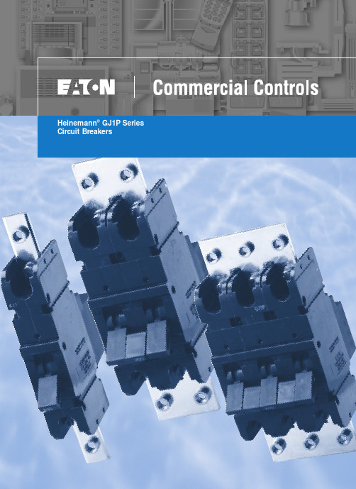
Heinemann®GJ1P Series Circuit BreakersDESCRIPTIONOptional Low-Voltage Shunt for Current MeteringEaton Corporation’s Cutler-Hammer series of Heinemann GJ1P breakers offer high quality circuit protection for DC applications from 100 to 1200 Amperes.Their precisely tailored time delays and ability to interrupt high currents makes them ideally suited for critical applications. On overloads exceeding 1000 – 1400% of rating, there is no intentional time delay and the breaker interrupts currents of as much as 25,000 A at 65V DC.An optional shunt (25 or 50millivolt full scale) permits metering of current. Since the shunt output is low voltage,light-gauge wiring can be used from shunt to meter.Indication may be displayed inpercent, watts, safe/danger or other dial calibrations. In addition, the busbar is available in two versions:Standard Size and Reduced Size. Contact your Eaton Sales Representative for more information.Precision Current Equalization (PCE) Circuit BreakersGJ1P breakers rated 250 to1200 A are built in parallel construction. Conventional parallel pole breakers can experience uneven current distribution because of variations in internalresistances. This condition can result in nuisance tripping since the higher current in one parallel branch has the same effect as an overload on the sensing element in that branch. Proprietary Precision Current Equalization (PCE)circuit breakers, on the other hand, allow for differences in internal resistances byautomatically distributing the current equally through the parallel current sensing elements, minimizing the danger of nuisance tripping.The UL listed series GJ1P (UL489) models are available in a choice of fast, medium or slow response times to accurately match load conditions. They can be ordered in “series trip ”, “mid-trip ” and “switch only ”constructions and are available front- or back-mounted, front- or back-connected, with optional auxiliary switches for signaling.HYDRAULIC-MAGNETIC BENEFITSThe magnetic/hydraulic load-sensing and time delaymechanisms used in GJ1P breakers are insensitive to changes in ambient or enclosure temperature.Therefore, GJ1P circuitbreakers are suited for service conditions encountered in telecommunications,transportation, air conditioning and other outdoor or “heat-loaded ” equipment.SPECIFICATIONSStandard Current Ratings:100, 125, 150, 175, 200, 225,250, 300, 350, 400, 450, 500,600, 700, 800, 900, 1000,1100, 1200 A.Standard Maximum Voltages:160V DC up to 700A65V DC from 701 to 1200A Breakers will be labeled with standard maximum (UL) voltage unless otherwise specified.Special Current Ratings:Any integral rating between 100and 1200 A DC. Consult factory for ordering information and metering shunt restrictions.Interrupting Capacities:UL Listed:10,000 A @ 160V DC 25,000 A @ 65V DC Non-UL:14,000 A @ 160V DC.Operating Temperature Range:-40°C to +85°C.Approximate Weight:1-pole (100-225A) 1.13kg (2.5lbs)2-pole (250-400A) 2.27kg (5lbs)3-pole (450-700A) 3.40kg (7.5lbs)4-pole (701-800A) 4.54kg (10lbs)5-pole (801-1000A) 5.67kg (12.5lbs)6-pole (1001-1200A) 6.80kg (15lbs)Weight may vary based on shunt and busbar.APPROVALSUL Listing:GJ1P breakers are UL listed per UL489. For CSA certification,consult application engineering.Description . . . . . . . . . . . . . .2Specifications . . . . . . . . . . . .2Approvals . . . . . . . . . . . . . . .2Time Delay Characteristics . . .3Dimensions . . . . . . . . . . . .4-5How to Order . . . . . . . . . . .6-7Additional Products. . . . . . . . .8TABLE OF CONTENTS PageHEINEMANN ®CIRCUIT BREAKERSGJ1P Series Circuit Breakers(100-1200 Amperes DC)2Heinemann is a registered trademark of the Eaton Corporation, Commercial Controls Business Unit.100150.01.001.1110100100010,000200300400500600700800900100011001200125C u rv e 1C u rv e 2C u rv e 3Current – Percent of Ampere RatingT r i p T i m e – S e c o n d sDC CURVES100150.01.001.1110100100010,000200300400500600700800900100011001200125Current – Percent of Ampere RatingT r i p T i m e – S e c o n d sINSTANT DELAY DC CURVE PPERCENT OF RATED CURRENT VS. TRIP DELAY AT 25ºCTIME DELAYCHARACTERISTICSTime delay, in all models,is inversely proportional to the magnitude of the overload, adjusting automatically to limit transient power to the load. On overloads exceeding 1,000 –1,400%, the circuit breaker trips without any deliberately imposed delay.Curve 1.Standard time delayis furnished unlessanother optional delay is specified. It is thepreferred characteristic for use where the load is composed of both resistive and inductive components.Curve 2.Medium time delayis for general usein mixed (inductive and resistive) circuits where the breaker rating is matched to the current carrying capacity of the mains.Curve 3.Short time delaypermits a very brief delay period before tripping.Curve P .Non-time delay breakersare available forapplications which cannot tolerate even brief transient overloads.These breakers have no time delay mechanism other than that imposed by the coil self-inductance and the inertia of the mechanism.Tripping specificationsThe time delay curves depict breaker response time vs. percent of rated load with no preloading.The function is plotted at an ambient temperature of 77°F (25°C) with the breaker in a vertical or wall-mounted position.Series GJ1P circuitbreakers will carry 100%of rated load continuously.Both time delay and non-time delay breakers may trip between 101%and 125% of rated load,and must trip at 125%and above.3% (sec)Delay 100%125%200%400%600%800%1000%Delay Max.1no trip 1100150206 1.7.065Delay Min.1no trip 110224 1.1.01.008Delay Max.2no trip 110153.8.28.055Delay Min.2no trip 12 2.5.5.18.01.008Delay Max.3no trip 10.8.19.08.047.038Delay Min.3no trip.44.13.03.015.01.008STANDARD FRONT-CONNECTED CONSTRUCTIONWire Range #6 to 250 MCM74.59(2.938)76.20(3.000)Aux. Terminals, Male Type Molex 02-09-2101, Model 1190-T(See Illustrations for Combinations)Shunt Terminals, Female TypeMolex 02-09-1101, Model 1189-T37.69(1.484)42.84(1.687)0.99 (0.390)71.42(2.812)#10-32 Inserts (4 Places)38.10(1.500)19.05(0.750)19.05(0.750)6.35 ± 0.38(0.250 ± 0.156)6.35 ± 0.38(0.250 ± 0.156)Panel Mounting Hole Distance for #10-32LINELOAD 75.38(2.968)5.53(0.218)59.91(2.359)32.13(1.266)5.53(0.219)“D ” Type Terminals as Shown180.97(7.125)41.27(1.625)4.74(0.188)58.67(2.313)41.27(1.625)41.27(1.625)263.52(10.375)29.36(1.156)7.14(0.281)78.56(3.094)59.13(2.328)28°±5°32°±5°ONOFFSee Optional Terminal ConfigurationWire Range #6to 250 MCM41.27(1.625)36.49(1.437)38.10(1.500)100 – 22 A250 – 400Width dimensions are as follows:100 – 225 38.1 (1.5)250 – 400 A 76.2 (3.0)450 – 700 A 114.3 (4.5)701 – 800A 142.4 (6.0)801 – 1000A 190.5 (7.5)1001 – 1200A228.6 (9.0)28.95(1.141)46.40(1.828)22.22(0.875)Fastener Mounted ThisSide of Bus Plate,Terminals are Front-Connected and Unit is Rear-Mounted.Fastener Mounted This Side of Bus Plate, Terminalsare Back-Connected and Unit is Panel-Mounted.60.32(2.375)7.92(0.312)3/8-16UNC -2B (4 per Unit)38.10(1.500)225.43 (8.875)Center to CenterOptional Terminal ConfigurationsHEINEMANN ®CIRCUIT BREAKERSGJ1P Series Circuit BreakersDIMENSIONSDimensions are given here only as a preliminary guide to specifying. Final engineeringdrawings should be made from the latest Heinemann drawings. Contact Customer Service Center.Tolerance:±0.79 (0.031) except where noted. For metric threads, contact Customer Service Center.DIMENSIONS APPROXIMATE IN MM (INCHES)431.75(1.250) Min.41.65(1.641) Max.19.05(0.750)7.51(0.297)7.51(0.297)7.51(0.297)16.66(0.656)Typ.29.36(1.156)29.36(1.156)48.41(1.906)48.41(1.906)67.46(2.656)67.46(2.656)38.10(1.500)38.10(1.500)38.10(1.500)38.10(1.500)19.05(0.750)19.05(0.750)19.05(0.750)22.23(0.875) Min.321.31(12.65) Max.78.96(3.109)Min. Typ.5.15(0.203)Dia. Typ.C100 – 225 A Ratings 226 – 400 A Ratings401 – 700 150A RatingsBA106.75(4.203)Typ.C LC L C L FRONT MOUNTING PANEL AND SUPPORT BRACKET115.08(4.531)76.98(3.031)38.1(1.500)38.1(1.500)71.42(2.912)5.94(0.234)Ref.5.15(0.203)Typ. Dia.65.02(2.562)59.13(2.328)(3-Pole)3PoleC L C L C L Holes Required When Breaker Is Front-Mounted2Pole1PoleAB C (2-Pole)(1-Pole)38.88(1.531)19.43(0.765)Mounting kits containing clips, brackets and necessary hardware and instructions are available (consult factory).009-18234 100 – 225 A 1.5 (1-pole wide)009-18235 250 – 400 A 3 (2-pole wide)009-18232 450 – 700 A 4.5 (3-pole wide)For 701-1200A devices, contact your Eaton Sales Representative for mounting kit part numbers.See Step (2)See Step (5)BACK MOUNTING CIRCUIT BREAKERBack mounting circuit breaker mounting instructions 1. Position circuit breaker to support brackets.2. Place mounting bracket in recess on front top portion of circuit breaker.3. Install four (4) #10-32 by 3-1/4" long screws through holes in mounting bracket and support structure.4. Install lock washer and nut on each of the screws and tighten.5. Place mounting bracket on front lower portion of circuit breaker.6. Install two (2) #10-32 by 5/8" screws through holes in mounting bracket and support structure.7. Repeat step 4.5DIMENSIONS APPROXIMATE IN MM (INCHES)NOTE: Standard size busbar is shown above. For the reduced size busbar, contact your Eaton Sales Representative for mounting dimensions.Series PrefixGJ1PSwitch (No Coil)Series Trip w/SPDT Aux. SwitchSeries Trip Series Trip and Mid-Trip Series Trip, Mid-Trip and SPST Alarm SwitchTerminal Location Back FrontInternal Circuit Metering ShuntNo Shunts Metering Shunt Metering ShuntB HCodeLocationInternal CircuitCodeDescriptionShuntCode—25mV 50mVP M N0-2-3-98-99-Series Prefix GJ1PTerminal LocationBInternal Circuit3-Metering ShuntPAdd each appropriate Number or Letter …HEINEMANN ®CIRCUIT BREAKERSGJ1P Series Circuit BreakersHOW TO ORDER — Series GJ1PTo determine your Complete Catalog Number , you must start with appropriate Series Prefix and add the appropriate Code Letters and/or Numbers as in the example below:SELECTION TABLE61Multi-pole construction – Consult factory.An auxiliary switch, if supplied, will be located in the right pole space. If the auxiliary switch is supplied in a breaker which has a metering shunt, it will be single-pole single throw (SPST). The single-pole double throw (SPDT) auxiliary switch can be supplied only in a breaker without a metering shunt.2Cannot be used on breaker containing metering shunt.3Only for breakers rated in excess of 250 A. Breakers up to 250 A without meteringshunt are available as standard GJ1 type breakers. Please consult Series GJ catalog.MarketUL-489TerminalsSolderless Connector Bus Bar ConnectionStandard Current Ratings 1AmpereTrip Curve 1123P0 – 1200(Add 0 before amp rating if less than 1000A.Example: 0700)-01-02-03-0PDescriptionCodeDEDUStandardCodeCurveCodeComplete Catalog Number: GJ1PB3-PEDU0700-02Terminal ConfigurationEUS/European ApprovalDUStandard Current Ratings 10700Trip Curves 1-024Add 0 before amp rating if less than 1000. For example: a 700A rating would bedesignated as 0700.The width of the breaker is determined by the current rating:100 – 225 A 1.5” (1-pole wide)250 – 400 A 3” (2-pole wide)450 – 700 A 4.5” (3-pole wide)701 – 800A 6” (4-pole wide)801 – 1000A 7.5” (5-pole wide)1001 – 1200A 9” (6-pole wide)5See page 3 for time delay characteristics and trip curve information.7© 2001 Eaton Corporation All Rights Reserved Printed in USAForm No. BR5401SE0002A / CSS 65322June 2001Commercial ControlsFor the Widest Selection of Circuit Protection, from 0.01 to 1200 Amperes, Look to Eaton.。
EMZ6.8E中文资料
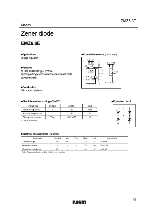
The products listed in this document are designed to be used with ordinary electronic equipment or devices (such as audio visual equipment, office-automation equipment, communications devices, electrical appliances and electronic toys). Should you intend to use these products with equipment or devices which require an extremely high level of reliability and the malfunction of with would directly endanger human life (such as medical instruments, transportation equipment, aerospace machinery, nuclear-reactor controllers, fuel controllers and other safety devices), please be sure to consult with our sales representative in advance. About Export Control Order in Japan Products described herein are the objects of controlled goods in Annex 1 (Item 16) of Export Trade Control Order in Japan. In case of export from Japan, please confirm if it applies to "objective" criteria or an "informed" (by MITI clause) on the basis of "catch all controls for Non-Proliferation of Weapons of Mass Destruction.
AM FM 海洋无线电台说明书
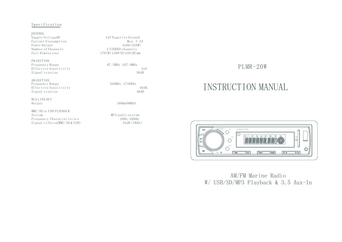
INSTRUCTION MANUALAM/FM Marine RadioW/USB/SD/MP3Playback & 3.5Aux-InPLMR-20WSpecificationGENERALFM SECTIONAM SECTIONRCA LINE OUT MMC/SD or USB PLAYBACK Supply VoltageDC 12V Negative GroundCurrent Consumption Max.7.5A Power Output4x60240W ()Number of Channels 2STEREO channels Unit Dimensions 178(W)x108(D)x50(H)mmFrequency Range87.5MHz 107.9MHzEffective Sensitivity 3uV.Signal to noise 50dBFrequency Range530KHz 1710KHzEffective Sensitivity 40dB.Output1000mV@MAX.SystemMP3audio systemFrequency 20Hz-20KHz Signal to Noise55dB (1KHz)Signal to noise 40dBCharacteristics(MMC/SD &USB)Page 2Page 1OPERATING THE UIIT1.-RESET BUTTON The unit must be reset under the following conditions:A)Prior to using this unit for the first time after installation.B)If the unit fails to operate properly,press the RESET with a pen tip or other pointed instrument.2.-SEL &VOL CONTROL BUTTONA)Press the SEL repeatedly to select VOLUME -BASS -TREBLE -BALANCE -FADER.B)Press and hold the SEL to select EQ(JASS -ROCK -POPS -CLASS -OFF)and LOUD(ON/OFF).3.-POWER ON/OFF AND MUTEPress the POWER to turn on this unit.To turn off theunit,press and hold this button unit it off.During playing,press this to mute the sound.9.-CLOCK BUTTON Press the CLK to show the time.To adjust the time,press and hold the CLK until flashing and change HOUR or MINUTE by rotate the >>I or I<<button.10-15.-PRESET STATIONS MEMORY AND >II,INT,RPT,RDM BUTTONS A)Radio mode Press the 1-6buttons to select the preset stations.Press and hold the 1-6buttons to store the station that currently listening.B)SD/MMC,and USB modePress the >II to pause or resume playing.Press the INT to play the first 10seconds of the tracks.Press again to off this function and the current track will keep playing.Press the RPT once to repeat plays the current track.Press the RPT twice to repeat plays the current folder.Press the RDM to turn random play on or off.Press the 5/6to move up or down 10tracks at a time (Note:when the remaining tracks less than 10,this function is invalid)WIRES CONNECTIONISO SOCKETANTENNA JACK ISO SOCKETSKETCHCONNECTOR B 1.VIOLET R.R SP(+)2.VIOLET BLACK R.R SP(-)3.GREY F.R SP(+)4.GREY BLACK F .R SP(-)57.GREEN R.L SP(+)8.GREEN BLACK R.L SP(-).WHITE F .L SP(+)6.WHITE BLACK F.L SP(-)INSTALLATION METHOD16.-AUX INPUT JACK (3.5MM STEREO JACK)Press the MODE to select auxiliary input playing mode when connecting with external audio device.17.-SD/MMC CARD SLOTWhen SD/MMC card is inserted,the unit isautomatically switched to SD/MMC mode.(Note:if both USB storage device and SD/MMC cardinserted,the system will switch to the mode of thelatest connected.)18.-USB PORTWhen USB storage device is connected,the unit is automatically switched to USB mode.4.-LCD DISPLAY5.-MODE BUTTONPress the MODE to select RADIO/CARD(SD/MMCcard inserted)/USB(flash driver inserted)/AUX mode.SD/MMC,and USB modePress and hold this button to activate TRACK SEARCHand play the select track automatically.6&7.-TUNE,SEEK,TRACK,SKIP UP/DOWN BUTTONSA)Radio modePress the>>I or I<<to perform manual seek tuning.Press and hold the >>I or I<<to perform automatictuning.The unit will tune to the station with strong signal.B)SD/MMC,and USB modePress the >>I or I<<to play the next or previous track.8.-BAND BUTTONPress the BND to select radio band as follow:FM1->FM2->FM3->AM1->AM2Press and hold the BND button to activate the auto storage function.The unit scans and preset thestations with strongest signal.(18stations in FM and 12stations in AM )CONNECTOR A 1.2.3.4.YELLOW MEMORY +12V5.BLUE AUTO ANTENNA B+6.7.RED POWER B+8.BLACK GROUND。
VMZ6.8N中文资料

ROHM : VMD3 EIAJ : − JEDEC : −
Absolute maximum ratings (Ta=25°C)
Parameter Power dissipation∗ Junction temperature Storage temperature Symbol
P
0.2±0.1
0.32±0.05
1.2±0.1
0∼0.1
0.13±0.05
Equivalent circuit
1/2
元器件交易网
VMZ6.8N
Diodes
Electrical characteristic curves (Ta=25°C)
CAPACITANCE BETWEEN TERMINALS : CT (pF)
6C
(3)
Features 1) Ultra small mold type. (VMD3) 2) Composite type with two anode common elements. 3) High reliability.
0.4
0.4
0.5±0.05
0.22±0.05
(2) (1)
0.8±0.1
Others
Parameter Device configuration IEC61000-4-2 Charge / discharge capacitance : 150pF Discharge resistance 10 repetitions Judgment contents No malfunction Contact Suspended : ±8kV : ±15kV : 330Ω
Appendix1-Rev1.0
REVERSE VOLTAGE : VR (V)
HZM96A仪表说明书-推荐下载

状态正式发布编号HN/QF.13-P029-003密级HZM96A型多功能电力数显仪表技术说明书A 版编制:张锦赵红梅校核:审定:批准:长沙华能自控集团说明本公司保留对此技术说明书所描述的产品规格进行修改的权利,恕不另行通知,不便之处敬请谅解。
订货前,请垂询本公司()或当地代理商以获悉本产品最新规格。
本产品的使用者应具备基本的电力常识。
在试图安装、操作或维护此设备之前,请仔细阅读本说明书。
在维护和检修之前,设备必须断电。
维护工作须由有资质的人员执行。
本说明书不适用于未受训者,在其正常使用范围之外所引起的问题,本公司概不负责。
目录说明 (1)一、产品介绍 (3)1简介 (3)2技术规格参数 (3)2.1 工作电源 (3)2.2 输入回路额定参数 (4)2.3 测量精度 (4)2.4 通讯 (4)2.5 绝缘性能 (4)2.6 抗电气干扰性 (5)2.7 环境条件 (5)二、安装指南 (6)1安装与接线 (6)1.1 盘面固定方法 (6)1.2 安装尺寸 (6)1.3 安装方法 (6)1.4外部接线说明 (7)1.5 接线方式 (8)2注意事项 (9)2.1 电压输入信号 (9)2.2 电流输入信号 (9)2.3 通讯接线 (9)3装置通电前检查 (10)4参数设置 (10)三、操作指南 (11)1显示介绍 (11)2操作说明 (11)3系统设置字符说明 (13)4系统及输入模式设置 (13)4.1 BUS状态设置 (13)4.2用户操作流程 (15)四、通信规约 (16)1通讯数据的类型与格式 (16)2通讯信息传输过程 (16)3功能码介绍 (17)3.1 功能码03 HEX:读取单路或多路寄存器数据 (17)4CRC校验 (18)5通讯错误信息及数据的处理 (19)6HZM96A仪表参量地址表 (19)一、产品介绍1 简介HZM96A仪表面向的用户群体广泛,适用于火电、热电、水电、电网、变电站(所)、泵站、水利枢纽等方面的电力自动控制和进行遥控遥测的电力调度远动系统,以及众多企事业单位用电、配电设备的现场电量监控等。
ZXMN6A08GTA;中文规格书,Datasheet资料

ZXMN6A08G60V SOT223 N-channel enhancement mode MOSFETSummaryDescriptionThis new generation trench MOSFET from Zetex features a unique structure combining the benefits of low on-resistance and fast switching, making it ideal for high efficiency power management applications.Features•Low on-resistance •Fast switching speed •Low threshold •Low gate drive •SOT223 packageApplications•DC-DC converters•Power management functions •Disconnect switches •Motor controlOrdering informationDevice markingZXMN 6A08V (BR)DSS R DS(on) (⍀)I D (A)600.080 @ V GS = 10V 5.30.150 @ V GS = 4.5V2.8DeviceReel size (inches)Tape width (mm)Quantity perreelZXMN6A08GTA 7121,000ZXMN6A08GTC13124,000Absolute maximum ratingsNOTES:(a)For a device surface mounted on 25mm x 25mm FR4 PCB with high coverage of single sided 1oz copper, in still air conditions.(b)For a device surface mounted on FR4 PCB measured at t Յ10 sec.(c)Repetitive rating - 25mm x 25mm FR4 PCB, D=0.02, pulse width 300s - pulse width limited by maximum junction temperature.ParameterSymbol Limit Unit Drain-source voltage V DSS 60V Gate-source voltage V GS ± 20V Continuous drain current@ V GS = 10V; T amb = 25°C (b)I D5.3A@ V GS = 10V; T amb = 70°C (b) 4.2@ V GS = 10V; T amb = 25°C (a)3.8Pulsed drain current (c)I DM 20A Continuous source current (body diode)(b)I S 2.1A Pulsed source current (body diode)(c)I SM 20A Power dissipation at T amb = 25°C (a) P D 2W Linear derating factor16mW/°C Power dissipation at T amb = 25°C (b) P D 3.9W Linear derating factor31mW/°C Operating and storage temperature rangeT j , T stg -55 to +150°C Thermal resistanceParameterSymbol Limit Unit Junction to ambient (a)R ⍜JA 62.5°C/W Junction to ambient (b)R ⍜JA32°C/WTypical characteristicsElectrical characteristics (at T amb = 25°C unless otherwise stated)Parameter SymbolMin.Typ.Max.UnitConditionsStaticDrain-source breakdown voltageV (BR)DSS 60V I D = 250A, V GS =0V Zero gate voltage drain currentI DSS 0.5A V DS = 60V, V GS =0V Gate-body leakage I GSS 100nA V GS =±20V, V DS =0V Gate-source threshold voltageV GS(th)1V I D = 250A, V DS =V GS Static drain-source on-state resistance (*)R DS(on)0.080⍀V GS = 10V, I D = 4.8A 0.150⍀V GS = 4.5V, I D = 4.2A Forward transconductance (*) (‡)NOTES:(*)Measured under pulsed conditions. Pulse width Յ300s; duty cycle Յ2%.g fs6.6SV DS = 15V, I D = 4.8ADynamic (‡)Input capacitance C iss 459pF V DS = 40V, V GS =0V f=1MHzOutput capacitanceC oss 44.2pF Reverse transfer capacitance C rss24.1pFSwitching (†) (‡)(†)Switching characteristics are independent of operating junction temperature.(‡)For design aid only, not subject to production testing.Turn-on delay time t d(on) 2.6ns V DD = 30V, I D = 1.5A R G ≅6.0⍀, V GS = 10VRise timet r 2.1ns Turn-off delay time t d(off)12.3ns Fall time t f 4.6ns Gate charge Q g 4.0nC V DS = 30V, V GS = 5V I D = 1.4ATotal gate charge Q g 5.8nC V DS = 30V, V GS = 10V I D = 1.4AGate-source charge Q gs 1.4nC Gate drain charge Q gd1.9nCSource-drain diode Diode forward voltage (*)V SD 0.88 1.2V T j =25°C, I S = 4A, V GS =0VReverse recovery time (‡)t rr 19.2ns Tj=25°C, I S = 1.4A,di/dt=100A/sReverse recovery charge (‡)Q rr30.3nCTypical characteristicsTypical characteristicsIntentionally left blankFor international sales offices visit /officesZetex products are distributed worldwide. For details, see /salesnetworkThis publication is issued to provide outline information only which (unless agreed by the company in writing) may not be used, applied or reproduced for any purpose or form part of any order or contact or be regarded as a representation relating to the products or services concerned.The company reserves the right to alter without notice the specification, design, price or conditions of supply of any product or service.EuropeZetex GmbHStreitfeldstraße 19D-81673 München GermanyTelefon: (49) 89 45 49 49 0Fax: (49) 89 45 49 49 49europe.sales@AmericasZetex Inc700 Veterans Memorial Highway Hauppauge, NY 11788USATelephone: (1) 631 360 2222Fax: (1) 631 360 8222usa.sales@Asia PacificZetex (Asia Ltd)3701-04 Metroplaza Tower 1Hing Fong Road, Kwai Fong Hong KongTelephone: (852) 26100 611Fax: (852) 24250 494asia.sales@Corporate HeadquartersZetex Semiconductors plcZetex Technology Park, Chadderton Oldham, OL9 9LL United KingdomTelephone: (44) 161 622 4444Fax: (44) 161 622 4446hq@Package outline - SOT223Note: Controlling dimensions are in millimeters. Approximate dimensions are provided in inchesDIM Millimeters Inches DIM Millimeters Inches Min Max Min Max MinMaxMinMaxA - 1.80-0.071e 2.30 BSC 0.0905 BSC A10.020.100.00080.004e1 4.60 BSC 0.181 BSC b 0.660.840.0260.033E 6.707.300.2640.287b2 2.90 3.100.1140.122E1 3.30 3.700.1300.146C 0.230.330.0090.013L 0.90-0.355-D6.306.700.2480.264-----分销商库存信息: DIODESZXMN6A08GTA。
FMAM

•
• 调频就是用调制信号x去控制高频载波信号的频率。
常用的是线性调频,即让调频信号的频率按调制信 号x的线性函数变化。调频信号us的一般表达式可写 为: 式中 Wc ── 载波信号的角频率; Um ── 调频信号中载波信号的幅度; m ── 调制度。 图X3-2绘出了这种调频信号的波形。图a为调制信 号x的波形,它可以按任意规律变化; 下图为调频信号 的波形.
• 收音机的基本工作原理
•
2. 在接收到我们所需收听的电台高频电波后,下 一步就是把“搭载”在电波上的声音信息取下来,这 个“搭载”过程叫调制,那么现在把声音信号取下来 则称为解调。解调是通过特别设计的电子线路来完成 的。调制的方式有调幅,调频,调相,相对应的,解调 的方式或采用的电子线路也是不相同的。从天线上直 接接收到的无线电信号是非常微弱的,在通过调谐电 路后还需经过放大电路放大到一定幅度才能送往解调 电路。 3. 从无线电波上解调出来的声音信息此时还是一 种幅度很低的电信号,我们人耳是听不到的,还需用 功率放大电路将其放大,再通过喇叭或耳机才能还原 成我们真正能听到的声音。
• •
通常无线电波所指的是从极低频3Hz到极超 高频的顶点30GHz(Giga Hertz), 国际短波广播波段 无线电广播和电视无线电波传播 AM: 中波广播使用的频段大致为526.5--1606.5kHz 短波广播使用的频段约为2.3--26.1MHz FM: 频率约为87--108MHz
调频(FM)与调幅(AM)
• 信号的调制
在信号调制中常以一个高频正弦信号作为载波信号。一 个正弦信号有幅值、频率、相位三个参数,可以对这三个 参数进行调制,分别称为调幅、调频和调相。也可以用脉 冲信号作载波信号。可以对脉冲信号的不同特征参数作调 制,最常用的是对脉冲的宽度进行调制,称为脉冲调宽。
- 1、下载文档前请自行甄别文档内容的完整性,平台不提供额外的编辑、内容补充、找答案等附加服务。
- 2、"仅部分预览"的文档,不可在线预览部分如存在完整性等问题,可反馈申请退款(可完整预览的文档不适用该条件!)。
- 3、如文档侵犯您的权益,请联系客服反馈,我们会尽快为您处理(人工客服工作时间:9:00-18:30)。
HZM6.8MWA
Silicon Planar Zener Diode for Surge Absorb
REJ03G1210-0200
(Previous: ADE-208-851A)
Rev.2.00
Jun 13, 2005 Features
• HZM6.8MWA has two devices in a monolithic, and can absorb surge.
• MPAK Package is suitable for high density surface mounting and high speed assembly.
Ordering Information
Type No. Laser Mark Package Name
Package Code (Previous Code)
HZM6.8MWA 68M MPAK PLSP0003ZC-A
(MPAK) Pin Arrangement
Absolute Maximum Ratings
(Ta = 25°C)
Value
Unit Item Symbol
Power dissipation Pd *1 200 mW
Junction temperature Tj 150 °C
Storage temperature Tstg −55 to +150 °C
Note: 1. Two device total, See Fig.2.
Electrical Characteristics *1
(Ta = 25°C)
Unit Test
Condition
Max
Typ
Item Symbol
Min
V
I Z = 5 mA, 40 ms pulse
7.0
—
Zener voltage V Z 6.47
µA V R = 3.5 V
2
—
Reverse current I R —
V R = 0 V, f = 1 MHz
130
pF
—
Capacitance C —
ΩI Z = 5 mA
30
Dynamic resistance r d —
—
ESD-Capability *2, *3 — 30 — — kV C = 150 pF, R = 330 Ω, Both forward
and reverse direction 10 pulse
Notes: 1. Per one device
2. Failure criterion ; I R > 2 µA at V R =
3.5 V.
Main Characteristic
Package Dimensions
RENESAS SALES OFFICES
Refer to "/en/network" for the latest and detailed information.
Renesas Technology America, Inc.
450 Holger Way, San Jose, CA 95134-1368, U.S.A
Tel: <1> (408) 382-7500, Fax: <1> (408) 382-7501
Renesas Technology Europe Limited
Dukes Meadow, Millboard Road, Bourne End, Buckinghamshire, SL8 5FH, U.K.
Tel: <44> (1628) 585-100, Fax: <44> (1628) 585-900
Renesas Technology Hong Kong Ltd.
7th Floor, North Tower, World Finance Centre, Harbour City, 1 Canton Road, Tsimshatsui, Kowloon, Hong Kong
Tel: <852> 2265-6688, Fax: <852> 2730-6071
Renesas Technology Taiwan Co., Ltd.
10th Floor, No.99, Fushing North Road, Taipei, Taiwan
Tel: <886> (2) 2715-2888, Fax: <886> (2) 2713-2999
Renesas Technology (Shanghai) Co., Ltd.
Unit2607 Ruijing Building, No.205 Maoming Road (S), Shanghai 200020, China
Tel: <86> (21) 6472-1001, Fax: <86> (21) 6415-2952
Renesas Technology Singapore Pte. Ltd.
1 Harbour Front Avenue, #06-10, Keppel Bay Tower, Singapore 098632
Tel: <65> 6213-0200, Fax: <65> 6278-8001。