asr01-intro
飞行伙伴LED闪光灯产品说明书

f l a s h l igh tU S E R M A N U A LUSERMANUALFLIGHTOUTFITTERS.COMfor more information and video demo:Th i sp r odu c t i sgua r an t eedaga i n s ta l lde f e c t s i nwo r kman s h i pandma t e r i a l sf o rt heo r i g i na lowne rf o roneyea r f r omt heda t eo fpu r c ha s e.Fo ranyadd i t i ona l i n f o rma t i on:Ca l lu sa t513-688-730,o rEma i lu sa the l p@F l i gh tOu tt t e r s.comYou’r enowwe l lequ i ppedt ohand l ea l lo fyou rc oc kp i t l i gh t i ngneed s.P l ea s er e f e r t ot hef o l l ow i ngmanua l f o ru s e r i n s t r u c t i on s.U.S.Pa t en t:D659.869STHANKYOUFORYOURPURCHASE!WARRANTYINFORMAT IONFLASHLIGHT OVERVIEW4X ADJUSTABLE ZOOM & STEALTH RINGLIGHT MODES & SPECIFICATIONSCONVEX LENSTACTICAL EDGEfive light modesS - STROBE H - HIGH M - MEDIUM L - LOWSL - STEALTH LIGHTORANGESTEALTH RINGANODIZED AIRCRAFT GRADE ALUMINUM; WATER ANDIMPACT-RESISTANT STEEL CLIPUSB IN/OUT PORTSMART SELECT DIALPOWERFULMAGNETIC BASEGLOW-IN-THE-DARK BUTTON WITH BATTERYINDICATORANTI-ROLL TACTICAL GRIP RING 4X ADJUSTABLEZOOM HEAT-SINK BEZEL The BUSH PILOT FLASHLIGHT is equipped with a Smart Select Dial to easily navigate the 5 lighting modes. Simply turn dial to align the arrow with the desired light mode. Light modes can be changed while light is ON or OFF.CHARGING YOUR USB MOBILE DEVICESTROBE HIGH MEDIUM LOW STEALTH LIGHT 2.5 hrs. 2.5 hrs. 4.5 hrs. 13 hrs. 120 hrs.120 meters 120 meters 85 meters 40 meters 4 metersstrobe: For emergency situations and distresssignaling, provides 2.5 hours of continuous use.stealth light: Provides low signature GREEN lightfrom the power button for low-pro le, stealth mode.short-range: Turn thehead of the ashlightclockwise for oodlight, perfect for short-rangelighting.usb power bank: Connect a compatible USB cable from your device to the USB port on ashlight.power bank status: When 1 steady RED LED & 1 GREEN blinking LED shows, this indicates that ashlight battery level is 25% or less. This allows you to decide to keep charging your device or maintain 25% power in the ashlight. Flashlight turns OFF at 10% to protect the battery from over draining.to use light when charging: Before connecting USB cable, turn select dial to “L” to activate LOW mode. Turn the dial to any other light mode to deactivate the light. Only LOW mode can be accessed during charging.long-range: Turn the head of the ashlight counter-clockwise for spotlight, perfect forfocusing light up to 120 meters.12run time & distance ratings+the ht, e he head of -clockwise for 20 meters.The BUSH PILOT FLASHLIGHT is equipped with a 4xadjustable zoom that changes from spotlight to oodlight with a simple twist of the bezel.focusing light up to 120 me 20 me The BUSH PILOT FLASHLIGHT isequipped with the signature orange ring, that will illuminate the four different light modes. To conceal this orange ring, turn the stealth ring clockwise and vice versa to reveal.CHARGING THE FLASHLIGHTTO REVEAL or TO HIDE THE USB CHARGING PORT:turn the Anti-Roll Tactical ring clockwise/counter-clockwiseconnect the supplied usbcable: One end into any USBport and the other end intothe USB port of the ashlight.charging mode: Whilecharging, a steady BLUE LED will come ON in the power button, to indicate ashlight is charging.charge completed: Once ashlight isfully charged (approx. 6.5 hrs), BLUE LED will turn OFF.to use light when charging: Before connecting USBcable, turn select dial to “L” to activate LOW mode. Turn the dial to any other light mode to deactivate the light. Only LOW mode can be accessed during charging.1234charging your flashlight b B ht.D will on, to ghtt..w ill ld with aing modes. Sim esired light mode. ght is ON or OFF.and distress us use.ht BATTERY CARE & REPLACEMENTTo open battery compartment, unscrew(counter-clockwise) the end cap where thebutton and magnetic base are located.Remove old battery, containing (1) pre-installed 18650Li-ion battery.Battery is designed for 500 life cycles. Before replacingwith new battery, make sure current battery is no longer holding charge. Remove and dispose of battery properly.Insert new battery (NEBO 6698BAT) as indicated by arrow. Make sure battery is facing the correct direction (arrow pointing towards the front). Reattach end cap by turning clockwise.battery assembly1234Note: Use only recommended battery type (NEBO 6698BAT).TO REVEAL or TO HIDE THE USB CHARGING PORT: turn the Anti-Roll Tactical ring clockwise/counter-clockwise to activate power bank: Hold ashlight power buttonfor 3 seconds to activate. 2 GREEN blinking LEDs in the power button will con rm charge mode.It b tt (NEBO 6698BAT)i di t d b AN G L R L G。
钬斺

• 如是后驱动的车辆容易甩尾,如是前驱动 的车辆容易方向失控。有ASR时,汽车在 加速时就不会有或能够减轻这种现象。在 转弯时,如果发生驱动轮打滑会导致整个 车辆向一侧偏移,当有ASR时就会使车辆 沿着正确的路线转向;最重要的是车辆转弯 时,一旦驱动轮打滑就会全车一侧偏移, 这在山路上极度危险的,有ASR的车辆一 般不会发生这种现象。
自动语音识别技术
• 自动语音识别技术(Automatic Speech Recognition)是一种将人的语音转换为文 本的技术。语音识别是一个多学科交叉的 领域,它与声学、语音学、语言学、数字 信号处理理论、信息论、计算机科学等众 多学科紧密相连。由于语音信号的多样性 和复杂性,目前的语音识别系统只能在一 定的限制条件下获得满意的性能,或者说 只能应用于某些特定的场合。
ASR的原理
• ASR是ABS的升级版,它在ABS上加装可膨胀液 压装置、增压泵、液压压力筒、第四个车轮速度 传感器,复杂的电子系统和带有其自身控制器的 电子加速系统。 • 在驱动轮打滑时ASR通过对比各轮子转速, 电子系统判断出驱动轮打滑,自动立刻减少节气 门进气量,降低引擎转速,从而减少动力输出, 对打滑的驱动轮进行制动。 • 减少打滑并保持轮胎与地面抓地力的最合适 的动力输出,这时候无论你怎么给油,在ASR介 入下,会输出最适合的动力。
ASR 恢复选项
• ASR 备份和 ASR 还原。您可以通过“备份” 实用程序中的“自动系统故障恢复准备向 导”来使用备份功能。“自动系统故障恢 复准备向导”能够备份系统状态数据、系 统服务、以及所有与操作系统组件相关的 磁盘。同时向导还会创建一张软盘,其中 包含有关备份、磁盘配置(包含基本卷和 动态卷)以及如何执行还原的信息。
标准I型遥控器灵敏度.doc说明书

安培特声磁eas标准I型操作灵敏度手册
进入系统
按PSW会显示0-100,按▲去键把它调到0-108(系统进入密码108),再按CON键后就已经进入系统.
怎样看系统里面的数据:
MIN对应数值查看:
按MIN键就会显示1-14数值,可查看调整,调整按▲(上下),调整范围是0-200之间,系统默认为40,数值越小越灵敏,按CON键可退出。
GN对应数值查看:
按GN键就会显示R-1数值,可查看调整,调整按▲(上下),调整范围是0-1之间,系统默认为1,数值是1灵敏度最高,按CON键可退出。
RE对应数值查看:
按RE键就会显示L-8数值,可查看调整,调整按▲(上下),调整范围是0-14之间,系统默认为4,数值越小灵敏度越高,按CON键可退出。
怎样看系统噪声值
系统共分两组噪声值,分别是D-1和D-2
进入系统以后,按NSE键后会出现D-0,按▲键把D-0调到D-1,再按CON键,就会出现第一组噪声值,噪声值越大环境干扰越大,容易出现误报。
同按以上操作把D-0调到D-2再按CON键,就会出现第二组噪声值。
灵敏度调整及噪声值降低方法
灵敏度跟系统噪声值是相反的,灵敏度越高噪声值越低,调整灵敏度方法:
1、首先将设备线路接好,接通电源查看系统噪声值,参考噪声值的说明,数值越接近
0越好,如果数值偏大,请查看设备周围环境干扰(包括接入电源是否唯一供给此
设备、周围是否有大的磁场、日光灯、有镇流器的设备)逐一排除。
2、灵敏度的增加和减少方法要分别调整GN ,RE,MIN三个对应数值,其中RE,MIN两
个数值越小灵敏度越高,GN数值为1灵敏度高。
安科ASR医疗器械产品
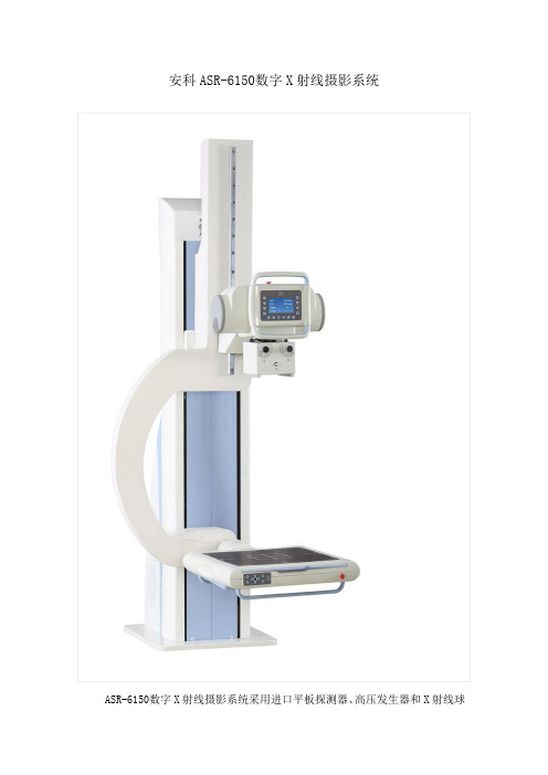
安科ASR-6150数字X射线摄影系统
ASR-6150数字X射线摄影系统采用进口平板探测器、高压发生器和X射线球
管,图像清晰细腻,成像快速;自动曝光系统,大大减少了患者的X射线吸收率;自主研发的操作软件界面清晰明了,操作简单,是一款顺应市场需求、性价比高的X射线摄影系统。
安科ASR-9150数字X射线摄影系统
ASR-9150精巧的U型臂CCD探测器与球管支撑系统,可以进行立位,卧位,坐姿和多种特殊投照角度的摄影,满足临床绝大部分的摄片要求; 高质量X线球管具有超高灵敏度和极高的可靠性、超长使用寿命等特点; 一体化控制台,提供DICOM标准接口,是性能价格比很高的多用途摄影系统,产品的各项技术性能达到国际先进水平。
安科移动式CT
移动CT一体化智能手术系统是国内首套移动CT图像和全身手术导航完美结合的综合性解决方案。
利用安科公司20多年的放射产品经验,国内领先的手术导航技术及深厚的医学领域积淀,将全身手术实时导航与术中即时影像一体化整合,创造了可靠的影像导航一体化复合手术系统,无缝集成了多种手术和诊断工具。
利用自由移动CT扫描获取图像,手术导航实时定位,彻底解决导航漂移问题,从而帮助医生实现病人精准手术,使手术计划更全面,操作更方便,效率更强大。
---弗锐达医疗器械咨询网。
微尔西半导体1微秒微电子公司2014年产品说明书
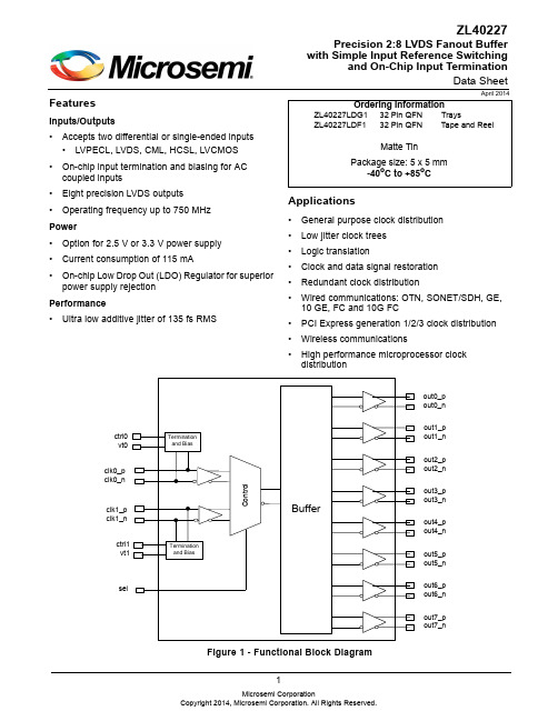
1FeaturesInputs/Outputs •Accepts two differential or single-ended inputs •LVPECL, LVDS, CML, HCSL, LVCMOS •On-chip input termination and biasing for AC coupled inputs•Eight precision LVDS outputs •Operating frequency up to 750 MHzPower •Option for 2.5 V or 3.3 V power supply •Current consumption of 115 mA•On-chip Low Drop Out (LDO) Regulator for superior power supply rejectionPerformance •Ultra low additive jitter of 135 fs RMSApplications•General purpose clock distribution •Low jitter clock trees •Logic translation•Clock and data signal restoration •Redundant clock distribution•Wired communications: OTN, SONET/SDH, GE, 10 GE, FC and 10G FC•PCI Express generation 1/2/3 clock distribution •Wireless communications•High performance microprocessor clock distributionApril 2014Figure 1 - Functional Block DiagramZL40227Precision 2:8 LVDS Fanout Buffer with Simple Input Reference Switchingand On-Chip Input TerminationData SheetOrdering InformationZL40227LDG1 32 Pin QFN TraysZL40227LDF132 Pin QFNTape and ReelMatte TinPackage size: 5 x 5 mm-40o C to +85o CTable of ContentsFeatures . . . . . . . . . . . . . . . . . . . . . . . . . . . . . . . . . . . . . . . . . . . . . . . . . . . . . . . . . . . . . . . . . . . . . . . . . . . . . . . . . 1 Applications . . . . . . . . . . . . . . . . . . . . . . . . . . . . . . . . . . . . . . . . . . . . . . . . . . . . . . . . . . . . . . . . . . . . . . . . . . . . . 1 Change Summary . . . . . . . . . . . . . . . . . . . . . . . . . . . . . . . . . . . . . . . . . . . . . . . . . . . . . . . . . . . . . . . . . . . . . . . . . 41.0 Package Description . . . . . . . . . . . . . . . . . . . . . . . . . . . . . . . . . . . . . . . . . . . . . . . . . . . . . . . . . . . . . . . . . . . .52.0 Pin Description. . . . . . . . . . . . . . . . . . . . . . . . . . . . . . . . . . . . . . . . . . . . . . . . . . . . . . . . . . . . . . . . . . . . . . . . .63.0 Functional Description . . . . . . . . . . . . . . . . . . . . . . . . . . . . . . . . . . . . . . . . . . . . . . . . . . . . . . . . . . . . . . . . . .73.1 Clock Inputs. . . . . . . . . . . . . . . . . . . . . . . . . . . . . . . . . . . . . . . . . . . . . . . . . . . . . . . . . . . . . . . . . . . . . . . . .73.1.1 Clock Input Selection. . . . . . . . . . . . . . . . . . . . . . . . . . . . . . . . . . . . . . . . . . . . . . . . . . . . . . . . . . . . .73.1.2 Clock Input Terminations. . . . . . . . . . . . . . . . . . . . . . . . . . . . . . . . . . . . . . . . . . . . . . . . . . . . . . . . . .73.2 Clock Outputs . . . . . . . . . . . . . . . . . . . . . . . . . . . . . . . . . . . . . . . . . . . . . . . . . . . . . . . . . . . . . . . . . . . . . .123.3 Device Additive Jitter. . . . . . . . . . . . . . . . . . . . . . . . . . . . . . . . . . . . . . . . . . . . . . . . . . . . . . . . . . . . . . . . .153.4 Power Supply . . . . . . . . . . . . . . . . . . . . . . . . . . . . . . . . . . . . . . . . . . . . . . . . . . . . . . . . . . . . . . . . . . . . . .163.4.1 Sensitivity to power supply noise. . . . . . . . . . . . . . . . . . . . . . . . . . . . . . . . . . . . . . . . . . . . . . . . . . .163.4.2 Power supply filtering. . . . . . . . . . . . . . . . . . . . . . . . . . . . . . . . . . . . . . . . . . . . . . . . . . . . . . . . . . . .163.4.3 PCB layout considerations. . . . . . . . . . . . . . . . . . . . . . . . . . . . . . . . . . . . . . . . . . . . . . . . . . . . . . . .164.0 AC and DC Electrical Characteristics . . . . . . . . . . . . . . . . . . . . . . . . . . . . . . . . . . . . . . . . . . . . . . . . . . . . .175.0 Performance Characterization . . . . . . . . . . . . . . . . . . . . . . . . . . . . . . . . . . . . . . . . . . . . . . . . . . . . . . . . . . .196.0 Typical Behavior . . . . . . . . . . . . . . . . . . . . . . . . . . . . . . . . . . . . . . . . . . . . . . . . . . . . . . . . . . . . . . . . . . . . . .207.0 Package Characteristics. . . . . . . . . . . . . . . . . . . . . . . . . . . . . . . . . . . . . . . . . . . . . . . . . . . . . . . . . . . . . . . .218.0 Mechanical Drawing . . . . . . . . . . . . . . . . . . . . . . . . . . . . . . . . . . . . . . . . . . . . . . . . . . . . . . . . . . . . . . . . . . .22List of FiguresFigure 1 - Functional Block Diagram . . . . . . . . . . . . . . . . . . . . . . . . . . . . . . . . . . . . . . . . . . . . . . . . . . . . . . . . . . . . 1 Figure 2 - Pin Connections . . . . . . . . . . . . . . . . . . . . . . . . . . . . . . . . . . . . . . . . . . . . . . . . . . . . . . . . . . . . . . . . . . . 5 Figure 3 - Simplified Diagram of Input Stage. . . . . . . . . . . . . . . . . . . . . . . . . . . . . . . . . . . . . . . . . . . . . . . . . . . . . . 7 Figure 4 - Clock Input - LVPECL - DC Coupled. . . . . . . . . . . . . . . . . . . . . . . . . . . . . . . . . . . . . . . . . . . . . . . . . . . . 8 Figure 5 - Clock Input - LVPECL - AC Coupled. . . . . . . . . . . . . . . . . . . . . . . . . . . . . . . . . . . . . . . . . . . . . . . . . . . . 8 Figure 6 - Clock Input - LVDS - DC Coupled . . . . . . . . . . . . . . . . . . . . . . . . . . . . . . . . . . . . . . . . . . . . . . . . . . . . . . 9 Figure 7 - Clock Input - LVDS - AC Coupled . . . . . . . . . . . . . . . . . . . . . . . . . . . . . . . . . . . . . . . . . . . . . . . . . . . . . . 9 Figure 8 - Clock Input - CML- AC Coupled . . . . . . . . . . . . . . . . . . . . . . . . . . . . . . . . . . . . . . . . . . . . . . . . . . . . . . 10 Figure 9 - Clock Input - HCSL- AC Coupled . . . . . . . . . . . . . . . . . . . . . . . . . . . . . . . . . . . . . . . . . . . . . . . . . . . . . 10 Figure 10 - Clock Input - AC-coupled Single-Ended . . . . . . . . . . . . . . . . . . . . . . . . . . . . . . . . . . . . . . . . . . . . . . . 11 Figure 11 - Clock Input - DC-coupled 3.3V CMOS. . . . . . . . . . . . . . . . . . . . . . . . . . . . . . . . . . . . . . . . . . . . . . . . . 11 Figure 12 - Simplified LVDS Output Driver. . . . . . . . . . . . . . . . . . . . . . . . . . . . . . . . . . . . . . . . . . . . . . . . . . . . . . . 12 Figure 13 - LVDS DC Coupled Termination (Internal Receiver Termination). . . . . . . . . . . . . . . . . . . . . . . . . . . . . 12 Figure 14 - LVDS DC Coupled Termination (External Receiver Termination) . . . . . . . . . . . . . . . . . . . . . . . . . . . . 13 Figure 15 - LVDS AC Coupled Termination . . . . . . . . . . . . . . . . . . . . . . . . . . . . . . . . . . . . . . . . . . . . . . . . . . . . . . 13 Figure 16 - LVDS AC Output Termination for CML Inputs . . . . . . . . . . . . . . . . . . . . . . . . . . . . . . . . . . . . . . . . . . . 14 Figure 17 - Additive Jitter. . . . . . . . . . . . . . . . . . . . . . . . . . . . . . . . . . . . . . . . . . . . . . . . . . . . . . . . . . . . . . . . . . . . 15 Figure 18 - Decoupling Connections for Power Pins. . . . . . . . . . . . . . . . . . . . . . . . . . . . . . . . . . . . . . . . . . . . . . . 16 Figure 19 - Differential Voltage Parameter. . . . . . . . . . . . . . . . . . . . . . . . . . . . . . . . . . . . . . . . . . . . . . . . . . . . . . . 18 Figure 20 - Input To Output Timing . . . . . . . . . . . . . . . . . . . . . . . . . . . . . . . . . . . . . . . . . . . . . . . . . . . . . . . . . . . . 18Change SummaryBelow are the changes from the February 2013 issue to the April 2014 issue:Page Item Change1Applications Added PCI Express clock distribution.6Pin Description Added exposed pad to Pin Description.8Figure 4 and Figure 5Removed 22 Ohm series resistors from Figure 4 and 5. Theseresistors are not required; however there is no impact toperformance if the resistors are included.18Figure 19Clarification of V ID and V OD.Below are the changes from the November 2012 issue to the February 2013 issue:Page Item Change8Figure 4Changed text to indicate the circuit is not recommended forVDD_driver=2.5V.12Figure 12Changed gate values to +/+ on the left and -/- on the right.1.0 Package DescriptionThe device is packaged in a 32 pin QFNFigure 2 - Pin Connections2.0 Pin DescriptionPin DescriptionPin # Name Description1,3, 6, 8clk0_p, clk0_n,clk1_p, clk1_nDifferential Input (Analog Input). Differential input signals.30, 29, 28, 27, 26, 25, 24, 23, 18, 17, 16, 15, 14, 13, 12, 11 out0_p, out0_nout1_p, out1_nout2_p, out2_nout3_p, out3_nout4_p, out4_nout5_p, out5_nout6_p, out6_nout7_p, out7_nDifferential Output (Analog Output). Differential outputs.9, 19,22, 32vdd Positive Supply Voltage. 2.5V DC or 3.3 V DC nominal.20, 21gnd Ground. 0 V.2, 7vt0, vt1On-Chip Input Termination Node (Analog).Center tap between internal 50 Ohmtermination resistors.For a DC coupled LVPECL input connect this pin through a resistor to ground; 50 Ohmsfor 3.3V LVPECL or 20 Ohms for 2.5V LVPECL.For a DC coupled LVDS input or for an AC coupled differential input, leave this pinunconnected.4, 5ctrl0, ctrl1Digital Control for On-Chip Input Termination (Input). Selects differential input mode;0: DC coupled LVPECL or LVDS modes1: AC coupled differential modesThese pins are internally pulled down to GND.10NC No Connection. Leave unconnected.31sel Input Select (Input). Selects the reference input that is buffered;0: clk01: clk1This pin is internally pulled down to GND.Exposed Pad Device GND.3.0 Functional DescriptionThe ZL40227 is an LVDS clock fanout buffer with eight output clock drivers capable of operating at frequencies up to 750 MHz.The ZL40227 provides an internal input termination network for DC and AC coupled inputs; optional input biasing for AC coupled inputs is also provided. The ZL40227 can accept DC coupled LVPECL or LVDS and AC coupled LVPECL and LVDS input signals, AC coupled CML or HCSL input signals, and single ended signals. A pin compatible device with external termination is also available.The ZL40227 is designed to fan out low-jitter reference clocks for wired or optical communications applications while adding minimal jitter to the clock signal. An internal linear power supply regulator and bulk capacitors minimize additive jitter due to power supply noise. The device operates from 2.5V+/-5% or 3.3V+/-5% supply. Its operation is guaranteed over the industrial temperature range -40°C to +85°C.The device block diagram is shown in Figure 1; its operation is described in the following sections.3.1 Clock InputsThe device has a differential input equipped with two on-chip 50 Ohm termination resistors arranged in series with a center tap. The input can accept many differential and single-ended signals with AC or DC coupling as appropriate. A control pin is available to enable internal biasing for AC coupled inputs. A block diagram of the input stage is in Figure 3.Receiverclk_n 50clk_pVt 50BiasctrlFigure 3 - Simplified Diagram of Input Stage3.1.1 Clock Input SelectionThe select line chooses which input clock is routed to the outputs.Table 1 - Input SelectionSel Active Input0 clk01clk13.1.2 Clock Input TerminationsThis following figures give the components values and configuration for the various circuits compatible with the input stage and the use of the Vt and ctrl pins in each case.In the following diagrams where the ctrl pin is "1" and the Vt pin is not connected, the Vt pin can be instead connected to V DD with a capacitor. A capacitor can also help in Figure 4 between Vt and V DD. This capacitor will minimize the noise at the point between the two internal termination resistors and improve the overall performance of the device.Figure 4 - Clock Input - LVPECL - DC CoupledFigure 5 - Clock Input - LVPECL - AC CoupledFigure 6 - Clock Input - LVDS - DC CoupledFigure 7 - Clock Input - LVDS - AC CoupledFigure 8 - Clock Input - CML- AC CoupledFigure 9 - Clock Input - HCSL- AC CoupledFigure 10 - Clock Input - AC-coupled Single-EndedFigure 11 - Clock Input - DC-coupled 3.3V CMOS3.2 Clock OutputsLVDS has lower signal swing than LVPECL which results in a low power consumption. A simplified diagram for the LVDS output stage is shown in Figure 12.Figure 12 - Simplified LVDS Output DriverThe methods to terminate the ZL40227 drivers are shown in the following figures.Figure 15 - LVDS AC Coupled TerminationFigure 16 - LVDS AC Output Termination for CML Inputs3.3 Device Additive JitterThe ZL40227 clock fanout buffer is not intended to filter clock jitter. The jitter performance of this type of device is characterized by its additive jitter. Additive jitter is the jitter the device would add to a hypothetical jitter-free clock as it passes through the device. The additive jitter of the ZL40227 is random and as such it is not correlated to the jitter of the input clock signal.The square of the resultant random RMS jitter at the output of the ZL40227 is equal to the sum of the squares of the various random RMS jitter sources including: input clock jitter; additive jitter of the buffer; and additive jitter due to power supply noise. There may be additional deterministic jitter sources, but they are not shown in Figure 17.Figure 17 - Additive Jitter3.4 Power SupplyThis device operates with either a 2.5V supply or 3.3V supply.3.4.1 Sensitivity to power supply noisePower supply noise from sources such as switching power supplies and high-power digital components such as FPGAs can induce additive jitter on clock buffer outputs. The ZL40227 is equipped with a low drop out (LDO) linear power regulator and on-chip bulk capacitors to minimize additive jitter due to power supply noise. The on-chip regulation, recommended power supply filtering, and good PCB layout all work together to minimize the additive jitter from power supply noise.3.4.2 Power supply filteringFor optimal jitter performance, the ZL40227 should be isolated from the power planes connected to its power supply pins as shown in Figure 18.•10 µF capacitors should be size 0603 or size 0805 X5R or X7R ceramic, 6.3 V minimum rating•0.1 µF capacitors should be size 0402 X5R ceramic, 6.3 V minimum rating•Capacitors should be placed next to the connected device power pinsFigure 18 - Decoupling Connections for Power Pins3.4.3 PCB layout considerationsThe power supply filtering shown in Figure 18 can be implemented either as a plane island, or as a routed power topology with the same performance.4.0 AC and DC Electrical CharacteristicsAbsolute Maximum Ratings*Parameter Sym.Min.Max.Units 1Supply voltage V DD_R-0.5 4.6V 2Voltage on any digital pin V PIN-0.5V DD V 4LVPECL output current I out30mA 5Soldering temperature T260 °C 6Storage temperature T ST-55125 °C 7Junction temperature T j125 °C 8Voltage on input pin V input V DD V 9Input capacitance each pin C p500fF * Exceeding these values may cause permanent damage. Functional operation under these conditions is not implied.* Voltages are with respect to ground (GND) unless otherwise statedRecommended Operating Conditions*Characteristics Sym.Min.Typ.Max.Units1Supply voltage 2.5 V mode V DD25 2.375 2.5 2.625V2Supply voltage 3.3 V mode V DD33 3.135 3.3 3.465V3Operating temperature T A-402585°C* Voltages are with respect to ground (GND) unless otherwise statedDC Electrical Characteristics - Current ConsumptionCharacteristics Sym.Min.Typ.Max.Units Notes 1Supply current LVDS drivers - loadedI dd_load115mA(all outputs are active)DC Electrical Characteristics - Inputs and Outputs - for 2.5/3.3 V SupplyCharacteristics Sym.Min.Typ.Max.Units Notes1CMOS control logic high-level inputV CIH0.7*V DD V voltageV CIL0.3*V DD V2CMOS control logic low-level inputvoltage3CMOS control logic Input leakageI IL1µA V I = V DD or 0 Vcurrent4Differential input common modeV ICM 1.1 1.6V for 2.5 voltageV ICM 1.1 2.0V for 3.35Differential input common modevoltage* The VOD parameter was measured from 125 MHz to 750 MHz.Figure 19 - Differential Voltage Parameter* Supply voltage and operating temperature are as per Recommended Operating ConditionsInputt Pt PWLt pdt PWHOutputFigure 20 - Input To Output Timing6Differential input voltage difference V ID 0.251V 7Differential input resistance V IR 80100120ohm 8LVDS output differential voltage*V OD 0.250.300.40V 9LVDS output common mode voltageV CM1.11.25 1.375VAC Electrical Characteristics* - Inputs and Outputs (see Figure 20) - for 2.5/3.3 V Supply.CharacteristicsSym.Min.Typ.Max.Units Notes1Maximum Operating Frequency 1/t p 750MHz 2Input to output clock propagation delay t pd 012ns 3Output to output skew t out2out 80150ps 4Part to part output skewt part2part 120300ps 5Output clock Duty Cycle degradation t PWH / t PWL-55Percent 6LVDS Output slew rate r sl 0.55V/ns 7Reference transition timet switch23usDC Electrical Characteristics - Inputs and Outputs - for 2.5/3.3 V SupplyCharacteristicsSym.Min.Typ.Max.Units NotesAdditive Jitter at 2.5 V*Output Frequency (MHz)Jitter MeasurementFilterTypical RMS (fs)Notes112512 kHz - 20 MHz 1842212.512 kHz - 20 MHz 1743311.0412 kHz - 20 MHz 157442512 kHz - 20 MHz 152550012 kHz - 20 MHz 1396622.0812 kHz - 20 MHz 138775012 kHz - 20 MHz135Additive Jitter at 3.3 V*Output Frequency (MHz)Jitter MeasurementFilterTypical RMS (fs)Notes112512 kHz - 20 MHz 1872212.512 kHz - 20 MHz 1763311.0412 kHz - 20 MHz 156442512 kHz - 20 MHz 153550012 kHz - 20 MHz 1406622.0812 kHz - 20 MHz 139775012 kHz - 20 MHz1375.0 Performance Characterization*The values in this table were taken with an approximate slew rate of 0.8 V/ns*The values in this table were taken with an approximate slew rate of 0.8 V/nsAdditive Jitter from a Power Supply Tone*Carrier frequencyParameterTypicalUnitsNotes125MHz 25 mV at 100 kHz 33fs RMS 750MHz25 mV at 100 kHz33fs RMS* The values in this table are the additive periodic jitter caused by an interfering tone typically caused by a switching power supply. For this test, measurements were taken over the full temperature and voltage range for V DD = 3.3 V. The magnitude of the interfering tone is measured at the DUT.6.0 Typical BehaviorTypical Waveform at 155.52 MHzV OD vs FrequencyPower Supply Tone Frequency versus PSRRPower Supply Tone Magnitude versus PSRRPropagation Delay versus TemperatureNote:This is for a single device. For more details, see thecharacterization section.7.0 Package CharacteristicsThermal DataParameter Symbol Test Condition Value UnitJunction to Ambient Thermal Resistance ΘJA Still Air1 m/s2 m/s 37.433.131.5o C/WJunction to Case Thermal Resistance ΘJC24.4o C/W Junction to Board Thermal Resistance ΘJB19.5o C/W Maximum Junction Temperature*T jmax125o C Maximum Ambient Temperature T A85o C© 2014 Microsemi Corporation. All rights reserved. Microsemi and the Microsemi logo are trademarks of Microsemi Corporation. All other trademarks and service marks are the property of their respective owners.Microsemi Corporation (NASDAQ: MSCC) offers a comprehensive portfolio of semiconductor and system solutions for communications, defense and security, aerospace and industrial markets. Products include high-performance and radiation-hardened analog mixed-signal integrated circuits, FPGAs, SoCs and ASICs; power management products; timing and synchronization devices and precise time solutions, setting the world’s standard for time; voice processing devices; RF solutions; discrete components; security technologies and scalable anti-tamper products; Power-over-Ethernet ICs and midspans; as well as custom design capabilities and services. Microsemi is headquartered in Aliso Viejo, Calif. and has approximately 3,400 employees globally. Learn more at .Microsemi Corporate Headquarters One One Enterprise, Aliso Viejo CA 92656 USA Within the USA: +1 (800) 713-4113Outside the USA: +1 (949) 380-6100Sales: +1 (949) 380-6136Fax: +1 (949) 215-4996E-mail: ***************************Information relating to products and services furnished herein by Microsemi Corporation or its subsidiaries (collectively “Microsemi”) is believed to be reliable. However, Microsemi assumes no liability for errors that may appear in this publication, or for liability otherwise arising from the application or use of any such information, product or service or for any infringement of patents or other intellectual property rights owned by third parties which may result from such application or use. Neither the supply of such information or purchase of product or service conveys any license, either express or implied, under patents or other intellectual property rights owned by Microsemi or licensed from third parties by Microsemi, whatsoever. Purchasers of products are also hereby notified that the use of product in certain ways or in combination with Microsemi, or non-Microsemi furnished goods or services may infringe patents or other intellectual property rights owned by Microsemi.This publication is issued to provide information only and (unless agreed by Microsemi in writing) may not be used, applied or reproduced for any purpose nor form part of any order or contract nor to be regarded as a representation relating to the products or services concerned. The products, their specifications, services and other information appearing in this publication are subject to change by Microsemi without notice. No warranty or guarantee express or implied is made regarding the capability, performance or suitability of any product or service. Information concerning possible methods of use is provided as a guide only and does not constitute any guarantee that such methods of use will be satisfactory in a specific piece of equipment. It is the user’s responsibility to fully determine the performance and suitability of any equipment using such information and to ensure that any publication or data used is up to date and has not been superseded. Manufacturing does not necessarily include testing of all functions or parameters. These products are not suitable for use in any medical and other products whose failure to perform may result in significant injury or death to the user. All products and materials are sold and services provided subject to Microsemi’s conditions of sale which are available on request.For more information about all Microsemi productsvisit our website at TECHNICAL DOCUMENTATION – NOT FOR RESALE。
Ra-01S规格书说明书
Ra-01S规格书版本V1.0版权©2020免责申明和版权公告本文中的信息,包括供参考的URL地址,如有变更,恕不另行通知。
文档“按现状”提供,不负任何担保责任,包括对适销性、适用于特定用途或非侵权性的任何担保,和任何提案、规格或样品在他处提到的任何担保。
本文档不负任何责任,包括使用本文档内信息产生的侵犯任何专利权行为的责任。
本文档在此未以禁止反言或其他方式授予任何知识产权使用许可,不管是明示许可还是暗示许可。
文中所得测试数据均为安信可实验室测试所得,实际结果可能略有差异。
文中提到的所有商标名称、商标和注册商标均属其各自所有者的财产,特此声明。
最终解释权归深圳市安信可科技有限公司所有。
注意由于产品版本升级或其他原因,本手册内容有可能变更。
深圳市安信可科技有限公司保留在没有任何通知或者提示的情况下对本手册的内容进行修改的权利。
本手册仅作为使用指导,深圳市安信可科技有限公司尽全力在本手册中提供准确的信息,但是深圳市安信可科技有限公司并不确保手册内容完全没有错误,本手册中的所有陈述、信息和建议也不构成任何明示或暗示的担保。
文件制定/修订/废止履历表版本日期制定/修订内容制定核准V1.02020.8.12首版徐目录一、产品概述 (5)二、电气参数 (7)三、外观尺寸 (9)四、管脚定义 (10)五、原理图 (11)六、设计指导 (12)七、回流焊曲线图 (14)八、包装信息 (15)九、联系我们 (15)一、产品概述安信可LoRa系列模块(Ra-01S)由安信可科技设计开发。
该模组用于超长距离扩频通信,其射频芯片SX1268主要采用LoRa™远程调制解调器,用于超长距离扩频通信,抗干扰性强,能够最大限度降低电流消耗。
借助SEMTECH的LoRa™专利调制技术,SX1268具有超过-148dBm的高灵敏度,+22dBm的功率输出,传输距离远,可靠性高。
同时,相对传统调制技术,LoRa™调制技术在抗阻塞和选择方面也具有明显优势,解决了传统设计方案无法同时兼顾距离、抗干扰和功耗的问题。
Microelectronics
RDA5802ES INGLE -C HIP B ROADCAST FM R ADIO T UNER Rev.1.7–Jun.20091 General DescriptionThe RDA5802Esingle-chip broadcast decoder. The tuner support The RDA5802E can frequency band.1.1Featuresl l Ø power supplyl Ø 65 -108 MHz l Digital low-IF tunerØ Image-reject down-converter Ø High performance A/D converter Ø IF selectivity performed internally l Fully integrated digital frequency synthesizerØ Fully integrated on-chip RF and IF VCO Ø Fully integrated on-chip loop filter l Autonomous search tuning l Support 32.768KHz crystal oscillator l Digital auto gain control (AGC) l Digital adaptive noise cancellationØ Mono/stereo switch Ø Soft mutel Line-level analog output voltagel 32.768 KHz 12M,24M,13M,26M,19.2M,38.4MHzReference clockl 2-wire and 3-wire serial control bus interface l Directly support 32Ω resistance loading l Integrated LDO regulatorØ 1.8 to 5.5 V operation voltage l 4X4mm 24 pin QFN package 1.2Applicationsl Cellular handsets l MP3, MP4 playersl Portable radios ,PDAs, NotebookFigure 1-1. RDA5802E Top View2 Table of Contents1General Description (1)1.1 Features (1)1.2Applications (1)2Table of Contents (2)3Functional Description (3)3.1 FM Receiver (3)3.2 Synthesizer (3)3.3 Power Supply (3)3.4 RESET and Control Interface select (4)3.5 Control Interface (4)3.6 I2S Audio Data Interface (4)3.7 GPIO Outputs (4)4Electrical Characteristics (5)5Receiver Characteristics (6)6Serial Interface (7)6.1 Three-wire Interface Timing (7)6.2 I2C Interface Timing (8)7Register Definition (9)8 Pins Description (13)9Application Diagram (15)9.1 Audio Loading Resistance Larger than 32Ω & TCXO Application: (15)9.1.1 Bill of Materials: (15)9.2 Audio Loading Resistance Lower than 32Ω & DCXO Application: (16)9.2.1 Bill of Materials: (16)10Package Physical Dimension (17)11PCB Land Pattern (18)12Change List (21)13Notes: (21)14RDA5802E与RDA5802对比 (22)15Contact Information (23)3Functional Descriptionconverters (ADCs), an audio DSP and a high- fidelity digital-to-analog converters (DACs). The LNA has differential input ports (LNAP and LNAN) and supports any input port by set according registers bits (LNA_PORT_SEL[1:0]). It default input common mode voltage is GND. The limiter prevents overloading and limits the amount of intermodulation products created by strong adjacent channels.The quadrature mixer down converts the LNA output differential RF signal to low-IF, it also has image-reject function.The PGA amplifies the mixer output IF signal and then digitized with ADCs.3.2SynthesizerThe frequency synthesizer generates the local oscillator signal which divide to quadrature, then be used to downconvert the RF input to a constant low intermediate frequency (IF). The synthesizer reference clock is 32.768 KHz. The synthesizer frequency is defined by bits CHAN[9:0] with the range from 65MHz to 108MHz. 3.3Power SupplyThe RDA5802E integrated one LDO which supplies power to the chip. The external supplyvoltage range is 1.8-5.5 V. 3.4RESET and Control Interface selectThe RDA5802E is RESET itself When VIO is Power up. And also support soft reset by trigger 02H BIT1 from 0 to 1. The control interface is select by MODE Pin. The MODE Pin is low ,I2C Interface is select. The MODE Pin is set to VIO, SPI Interface is select. 3.5Control InterfaceThe RDA5802E supports three- wire and I 2C control interface. User could select either of them to program the chip.The three-wireinterface. It includes 4-bit high register at posedge of SCLK. (MSB is the first bit) around cycle between and data from The I 2C interface SDIO. A I 2a 7-bit chip address The ACK (or NACK) is always sent out by receiver. When in write transfer, data bytes is written out from MCU, and when in read transfer, data bytes is read out from RDA5802E. There is no visible register address in I 2C interface transfers. The I 2C interface has a fixed start register address (0x02h for write transfer and 0x0Ah for read transfer), and an internal incremental address counter. If register address meets the end of register file, 0x3Ah, register address will wrap back to 0x00h. For writetransfer, MCU programs registers from register 0x02h high byte, then register 0x02h low byte, then register 0x03h high byte, till the last register. RDA5802E always gives out ACK after every byte, and MCU gives out STOP condition when register programming is finished. For read transfer, after command byte from MCU, RDA5802E sends out register 0x0Ah high byte, then register 0x0Ah low byte, then register 0x0Bh high byte, till receives NACK from MCU. MCU gives out ACK for data bytes besides last data byte. MCU gives out NACK for last data byte, and then RDA5802E will return the bus to MCU, and MCU will give out STOP condition.Details refer to RDA5802E Programming Guide . 2is fully compliant as I 2S master and rate is 48Kbps ,also support as . with bits GPIO1[1:0], pins could be and stereo indicator with bits GPIO1[1:0], GPIO2[1:0], GPIO3[1:0]. GPIO2 could be programmed to output a low interrupt (interrupt will be generated only with interrupt enable bit STCIEN is set to high) when seek/tune process completes. GPIO3 could be programmed to output stereo indicator bit ST. Constant low, high or high-Z functionality is available regardless of the state of VA and VD supplies or the ENABLE bit.Figure 3-2. I2S Digital Audio Format4 Electrical CharacteristicsTable 4-1DC Electrical Specification (Recommended Operation Conditions):1. For Pin: SCLK, SDIO, SEN, MODETable 4-3 Power Consumption Specification(VDD = 1.8 to 5.5 V, T A = -25 to 85 ℃, unless otherwise specified)SYMBOLDESCRIPTIONCONDITIONTYP UNIT I A Analog Supply Current ENABLE=1 18 mA I D Digital Supply Current ENABLE=13mA I VIO Interface Supply Current SCLK and RCLK inactive 90 µA I APD Analog Powerdown Current ENABLE=0 2 µA I DPD Digital Powerdown Current ENABLE=0 2 µA I VIOInterface Powerdown CurrentENABLE=010µASCK5 Receiver CharacteristicsTable 5-1 Receiver Characteristics(VDD = 2.7 to 5.5 V, T A = -25 to 85 °C, unless otherwise specified)Notes:1. F in=65 to 108MHz; F mod=1KHz; de-emphasis=75µs; MONO=1; L=R unless noted otherwise;2. ∆f=22.5KHz;3. B AF = 300Hz to 15KHz, RBW <=10Hz;4. |f2-f1|>1MHz, f0=2xf1-f2, AGC disable, F in=76 to 108MHz;5. P RF=60dB U V;6. ∆f=75KHz.7. Measured at V EMF = 1 m V, f RF = 65 to 108MHz8. At LOUT and ROUT pins6 Serial Interface6.1 Three-wire Interface TimingTable 6-1 Three-wire Interface Timing Characteristics(VDD = 2.7 to 5.5 V, T A = -25 to 85 °C, unless otherwise specified)Figure 6-2. Three-wire Interface Read Timing Diagram6.2 I2C Interface TimingTable 6-2 I2C Interface Timing Characteristics(VDD = 2.7 to 5.5 V, T A = -25 to 85 °C, unless otherwise specified)Figure 6-3. I2C Interface Write Timing DiagramFigure 6-4. I2C Interface Read Timing Diagram7 Register Definition8 Pins DescriptionN DCCP I O 1P I O 2P I O 3Table 8-2 Internal Pin Configuration9 Application Diagram9.1 Audio Loading Resistance Larger than 32Ω & TCXO Application:Ω Resistance1—I2C,VIO—SPI);7COMPONENT VALUE DESCRIPTION SUPPLIERU1 RDA5802E Broadcast FM Radio Tuner RDAJ1 Common 32Ω Resistance HeadphoneC2 100pF Couple CAP MurataL3/C3 100nH/24pF LC Chock for LNA Input MurataC4,C5 125µF Audio AC Couple Capacitors MurataC6 24nF Power Supply Bypass Capacitor MurataF1/F2 1.5K@100MHz FM Band Ferrite Murata9.2 Audio Loading Resistance Lower than 32Ω & DCXO Application:1310 Package Physical DimensionFigure 10-1illustrates the package details for the RDA5802E. The package is lead-free and RoHS-compliant.Figure 10-2. 24-Pin 4x4 Quad Flat No-Lead (QFN)11 PCB Land PatternTable-I Classification Reflow ProfilesPackage Thickness Volume mm3<350Volume mm3≥350<2.5mm 240 + 0/-5 o C 225 + 0/-5 o C≥2.5mm225 + 0/-5 o C225 + 0/-5 o CTable – II SnPb Eutectic Process – Package Peak Reflow Temperaturesthickness and volume. The use of convection reflow processes reduces the thermal gradients between packages. However, thermal gradients due to differences in thermal mass of SMD package may sill exist.Note 5: Components intended for use in a “lead-free” assembly process shall be evaluated using the “lead free”classification temperatures and profiles defined in Table-I II III whether or not lead free.RoHS CompliantThe product does not contain lead, mercury, cadmium, hexavalent chromium, polybrominated biphenyls (PBB) or polybrominated diphenyl ethers (PBDE), and are therefore considered RoHS compliant.ESD SensitivityIntegrated circuits are ESD sensitive and can be damaged by static electricity. Proper ESD techniques should be used when handling these devices.12 Change ListREV DATE AUTHER CHANGE DESCRIPTION V1.0 2009-03-03 ChunZhao Original Draft.13 Notes:1: 通过硬件电路设置芯片工作总线控制模式,详细电路如下图:14 RDA5802E与RDA5802对比1、5802E的0x0Ch=5803、0x0Dh=5804,可以通过读这两个寄存器的缺省值来区别5800、5802和5802E;2、FM天线尽量用第4脚(LNAP),不要用第2脚(LNAN)。
3512B 培训

HongKong
Taipei
LSHM CEL CML ECIM WesTrac
卡特彼勒公司的代理制 Our Dealers
中国区代理
LSHM (利星行机械): 江、浙、沪,鄂、豫、皖,鲁 CEL (信昌机器): 粤、闽、赣,湘、桂、疆,海南 WesTrac(威斯特): 京、津、冀,辽、吉、黑,晋、蒙 ECIM (易初明通): 云、贵、川,陕、甘、青,宁、藏 CML (中华机械): 台湾
电控调速、监控、报警、保护。 D=170,S=190,Vh=4.31L/缸(Vtot=51.8L),
SAE标准旋向,
发火序与各缸的识别。 系列机型参数见Front and TMI engine test result 3) 零部件, 系统结构和功能
Engine Division Facilitie主要发动机生产工厂
Cat China Rep Office
Shunde Guangzhou MaK Diesel Engine Co., Ltd.
Yunnan
Guizhou
Hunan
Jiangxi Fujian
Guangxi
Guangdong
Kunshan Lei Shing Hong Machinery
Cat China Training Center Taiwan
• 目前的多元化产品结 构,有17大类数百品种, 涵盖工程,建筑,矿山, 道路与非道路运输,林 业,石油,农机等行业.
• 发动机产业占1/3强.
• 目前3500B已成为卡 特彼勒公司柴油机的 主力机型
卡特彼勒发动机简介
• 1。CAT发动机
• 卡特彼勒公司不仅是世界最大的工程机械制造公司而且是最大的多用途发动机制造公 司,自1925年成立起,就自给自用发动机;
- 1、下载文档前请自行甄别文档内容的完整性,平台不提供额外的编辑、内容补充、找答案等附加服务。
- 2、"仅部分预览"的文档,不可在线预览部分如存在完整性等问题,可反馈申请退款(可完整预览的文档不适用该条件!)。
- 3、如文档侵犯您的权益,请联系客服反馈,我们会尽快为您处理(人工客服工作时间:9:00-18:30)。
ASR Lecture 1
Automatic Speech Recognition: Introduction
7
Variability in speech recognition
Several sources of variation Size Number of word types in vocabulary, perplexity Speaker Tuned for a particular speaker, or speaker-independent? Adaptation to speaker characteristics and accent Acoustic environment Noise, competing speakers, channel conditions (microphone, phone line, room acoustics) Style Continuously spoken or isolated? Planned monologue or spontaneous conversation?
Exam in April or May (worth 70%) Coursework (worth 30%, building on the lab sessions): out on 13 February; in by 8 March
People:
Lecturers: Steve Renals, Hiroshi Shimodaira TA: Joachim Fainberg Lab demonstrator: Ondrej Klejch
ASR Lecture 1
Automatic Speech Recognition: Introduction
5
Why is speech recognition difficult?
ASR Lecture 1
n: Introduction
6
Variability in speech recognition
Automatic Speech Recognition: Introduction
Steve Renals & Hiroshi Shimodaira
Automatic Speech Recognition— ASR Lecture 1 16 January 2017
ASR Lecture 1
Automatic Speech Recognition: Introduction
ASR Lecture 1
Automatic Speech Recognition: Introduction
3
Labs
Series of weekly labs using Kaldi. Choose one of
Tuesdays 10–11am Wednesdays 3-4pm
Select your lab time on doodle: /poll/cseti6wr95e86ac5 Labs will be in Forrest Hill, room 3.D01 Labs start week 2 (next week) Note: Training speech recognisers can take time
NO n oh
HMM
Acoustics X
ASR Lecture 1
Automatic Speech Recognition: Introduction
8
“Fundamental Equation of Statistical Speech Recognition”
If X is the sequence of acoustic feature vectors (observations) and W denotes a word sequence, the most likely word sequence W∗ is given by
ASR Lecture 1
Automatic Speech Recognition: Introduction
7
Variability in speech recognition
Several sources of variation Size Number of word types in vocabulary, perplexity Speaker Tuned for a particular speaker, or speaker-independent? Adaptation to speaker characteristics and accent Acoustic environment Noise, competing speakers, channel conditions (microphone, phone line, room acoustics)
W∗ = arg max P (W | X)
W
Applying Bayes’ Theorem: P (W | X) = p (X | W)P (W) p (X) ∝ p (X | W)P (W)
W
W∗ = arg max p (X | W) Acoustic model
ASR Lecture 1
P (W ) Language model
Several sources of variation Size Number of word types in vocabulary, perplexity
ASR Lecture 1
Automatic Speech Recognition: Introduction
7
Variability in speech recognition
Perfect!
either of (MLPR or MLP) but not Speech Processing
You’ll require some speech background:
A couple of the lectures will cover material that was in Speech Processing Some additional background study (including material from Speech Processing)
ASR Lecture 1
Automatic Speech Recognition: Introduction
4
What is speech recognition?
Speech-to-text transcription Transform recorded audio into a sequence of words Just the words, no meaning.... But do need to deal with acoustic ambiguity: “Recognise speech?” or “Wreck a nice beach?” Speaker diarization: Who spoke when? Speech recognition: what did they say? Paralinguistic aspects: how did they say it? (timing, intonation, voice quality) Speech understanding: what does it mean?
/teaching/courses/asr/
ASR Lecture 1 Automatic Speech Recognition: Introduction 2
Your background
If you have taken: Speech Processing and either of (MLPR or MLP)
1
Automatic Speech Recognition — ASR
Course details Lectures: About 18 lectures, plus a couple of extra lectures on basic introduction to neural networks Labs: Weekly lab sessions – using Kaldi () to build speech recognition systems. Assessment:
ASR Lecture 1
Automatic Speech Recognition: Introduction
8
Hierarchical modelling of speech
Generative Model "No right" RIGHT r ai t Utterance W Word Subword
Several sources of variation Size Number of word types in vocabulary, perplexity Speaker Tuned for a particular speaker, or speaker-independent? Adaptation to speaker characteristics and accent
9
Automatic Speech Recognition: Introduction
Speech Recognition Components
W∗ = arg max p (X | W)P (W)
W
Use an acoustic model, language model, and lexicon to obtain the most probable word sequence W∗ given the observed acoustics X