Valence band electronic structure of Pr1
紫外可见漫反射求带隙宽度
紫外可见漫反射求带隙宽度1. 引言紫外可见漫反射(UV-Vis diffuse reflectance spectroscopy)是一种常用的光谱分析技术,用于研究材料的光学性质。
在材料科学和化学领域,紫外可见漫反射可以用来确定材料的带隙宽度。
带隙宽度是指能带结构中价带(valence band)和导带(conduction band)之间的能级差。
它是一个重要的材料参数,对于了解材料的电子结构和光学性质具有重要意义。
本文将详细介绍紫外可见漫反射原理、带隙宽度的计算方法以及实际应用。
2. 紫外可见漫反射原理紫外可见漫反射是一种非常灵敏的光谱测量技术,通过测量样品对入射光的反射率来获取信息。
在紫外可见光谱范围内,材料的反射率与能带结构和电子能级密切相关。
当光线照射到材料表面时,一部分光被吸收,一部分光被反射。
被吸收的光能量会激发材料中的电子,使其从价带跃迁到导带。
根据库仑定律,当光通过材料时,电子会发生振荡,产生漫反射。
漫反射光的强度与材料的能带结构和电子态密度有关。
通过测量样品对入射光的漫反射光强度,可以得到材料的光谱信息。
3. 带隙宽度的计算方法带隙宽度可以通过紫外可见漫反射光谱的分析来计算。
在紫外可见光谱范围内,材料的反射率与波长有关,可以通过绘制反射率-波长曲线来分析材料的光学性质。
3.1 Kubelka-Munk理论Kubelka-Munk理论是一种常用的分析紫外可见漫反射光谱的方法。
该理论假设材料的吸收和散射是独立的。
根据Kubelka-Munk理论,漫反射光强度(R)与样品的吸收系数(α)和散射系数(S)之间存在以下关系:R = (1 - R∞)^2 / (2 * S * α)其中,R∞为样品的透射率。
3.2 Tauc方程Tauc方程是根据材料的能带结构推导出来的,用于计算带隙宽度。
根据Tauc方程,材料的吸收系数与入射光的能量之间存在以下关系:αhν = A(hν - Eg)^n其中,α为吸收系数,hν为入射光的能量,Eg为带隙宽度,A为常数,n为指数。
半导体物理器件与工艺英文原版
半导体物理器件与工艺英文原版Semiconductor Physics, Devices, and Fabrication.Introduction.Semiconductors are materials with electricalconductivity between that of conductors and insulators.This unique property makes them essential for a wide rangeof electronic devices, including transistors, diodes, and solar cells.Semiconductor Physics.The electrical properties of semiconductors are determined by their electronic band structure. In an insulator, the valence band (the band of electrons that are tightly bound to the atoms) is filled, and the conduction band (the band of electrons that are free to move) is empty. In a conductor, the conduction band is partially filled. In a semiconductor, the conduction band is empty and thevalence band is filled, but there is a small energy gap between the two bands.When a semiconductor is exposed to light or heat, electrons can be excited from the valence band to the conduction band. These electrons are then free to move, and the semiconductor becomes more conductive. This phenomenon is known as intrinsic conduction.Semiconductors can also be doped with impurities to increase their conductivity. Donor impurities add electrons to the semiconductor, while acceptor impurities remove electrons. Doped semiconductors are used to create transistors, diodes, and other electronic devices.Semiconductor Devices.Transistors are the basic building blocks of electronic circuits. They can be used to amplify signals, switch currents, and store data. Transistors are made from three layers of semiconductor material: the emitter, the base, and the collector.Diodes are another important type of semiconductor device. They allow current to flow in one direction but not the other. Diodes are used in a variety of applications, including rectifying AC currents and protecting circuits from overvoltage.Solar cells are semiconductor devices that convertlight into electricity. Solar cells are made from photovoltaic materials, which are materials that generate an electrical current when exposed to light. Solar cells are used to power a variety of devices, including calculators, watches, and satellites.Semiconductor Fabrication.Semiconductors are fabricated using a variety of processes, including lithography, etching, and deposition.Lithography is the process of creating patterns in semiconductor materials. Lithography is used to create the features of transistors, diodes, and other electronicdevices.Etching is the process of removing material from semiconductor wafers. Etching is used to create the trenches and vias that connect the different layers of a semiconductor device.Deposition is the process of adding material to semiconductor wafers. Deposition is used to create the metal layers that connect the different parts of a semiconductor device.Semiconductor fabrication is a complex and precise process. The quality of the final product depends on the accuracy of each step in the fabrication process.Conclusion.Semiconductors are essential for a wide range of electronic devices. The physics of semiconductors and the processes used to fabricate semiconductor devices are complex and challenging, but they are also essential forthe development of new and innovative electronic technologies.。
半导体基础

2. 复合与非平衡载流子寿命τ
复合是指电子与空穴相遇时,成对消失,以热或 发光方式释放出多余的能量。 非平衡载流子寿命τ:非平衡载流子从产生到复合 之前的平均存在时间。 它表征复合的强弱,τ小表示复合快,τ大表示复 合慢。它决定了光电器件的时间特性,采用光激 发方式的光生载流子寿命与光电转换的效果有直 接关系。τ的大小与材料的微观复合结构、掺杂、 缺陷有关。
本征吸收与非本征吸收:
本征吸收: 半导体吸收光子的能量使价带中的电子激发到导带,在价 带中留下空穴,产生等量的电子与空穴,这种吸收过程叫 本征吸收。 产生本征吸收的条件:入射光子的能量(hν)至少要等于 材料的禁带宽度Eg。即 hν≥Eg 从而有 ν0≥Eg/h λ0≤hc/Eg=1.24μm·eV/Eg h:普朗克常数;c:光速; ν0:材料的频率阈值;λ0:材料的波长阈值。
电子共有化,能级扩展为能带示意图 a) 单个原子 b) N个原子
禁带(Forbidden Band): 允许被电子占据的能带称为允许带,允许带之间的范 围是不允许电子占据的,此范围称为禁带。 原子壳层中的内层允许带总是被电子先占满,然后再 占据能量更高的外面一层的允许带。被电子占满的允 许带称为满带,每一个能级上都没有电子的能带称为 空带。 价带(Valence Band):原子中最外层的电子称为 价电子,与价电子能级相对应的能带称为价带。 导带(Conduction Band):价带以上能量最低的 允许带称为导带。 导带的底能级表示为Ec,价带的顶能级表示为Ev,Ec 与Ev之间的能量间隔称为禁带Eg。
0.92 0.55
非本征吸收:
非本征吸收包括杂质吸收、自由载流子吸收、激 子吸收和晶格吸收等。 杂质吸收:杂质能级上的电子(或空穴)吸收光 子能量从杂质能级跃迁到导带(空穴跃迁到价 带),这种吸收称为杂质吸收。杂质吸收的波长 阈值多在红外区或远红外区。 自由载流子吸收:导带内的电子或价带内的空穴 也能吸收光子能量,使它在本能带内由低能级迁 移到高能级,这种吸收称为自由载流子吸收,表 现为红外吸收。
(2021年整理)材料专业常用术语英语单词表

材料专业常用术语英语单词表编辑整理:尊敬的读者朋友们:这里是精品文档编辑中心,本文档内容是由我和我的同事精心编辑整理后发布的,发布之前我们对文中内容进行仔细校对,但是难免会有疏漏的地方,但是任然希望(材料专业常用术语英语单词表)的内容能够给您的工作和学习带来便利。
同时也真诚的希望收到您的建议和反馈,这将是我们进步的源泉,前进的动力。
本文可编辑可修改,如果觉得对您有帮助请收藏以便随时查阅,最后祝您生活愉快业绩进步,以下为材料专业常用术语英语单词表的全部内容。
Unit 1property (材料的)性质heat treatment 热处理metal 金属glass 玻璃plastics 塑料fiber 纤维electronic devices 电子器件component 组元,组分semiconducting materials 半导体材料materials science and engineering 材料科学与工程materials science 材料科学materials engineering 材料工程materials scientist 材料科学家materials engineer 材料工程师synthesize 合成synthesissubatomic structure 亚原子结构electron 电子atom 原子nuclei 原子核nucleusmolecule 分子microscopic 微观的microscope 显微镜naked eye 裸眼macroscopic 宏观的specimen 试样deformation 变形polished 抛光的reflect 反射magnitude 量级solid materials 固体材料mechanical properties 力学性质force 力elastic modulus 弹性模量strength 强度electrical properties 电学性质electrical conductivity 导电性dielectric constant 介电常数electric field 电场thermal behavior 热学行为heat capacity 热容thermal conductivity 热传导(导热性)magnetic properties 磁学性质magnetic field 磁场optical properties 光学性质electromagnetic radiation 电磁辐射light radiation 光辐射index of refraction 折射率reflectivity 反射率deteriorative characteristics 劣化特性processing 加工performance 性能linear 线性的integrated circuit chip 集成电路芯片strength 强度ductility 延展性deterioration 恶化,劣化mechanical strength 机械强度elevated temperature 高温corrosive 腐蚀性的fabrication 制造Unit 2chemical makeup 化学组成atomic structure 原子结构advanced materials 先进材料high-technology 高技术smart materials 智能材料nanoengineered materials 纳米工程材料metallic materials 金属材料nonlocalized electrons 游离电子conductor 导体electricity 电heat 热transparent 透明的visible light 可见光polished 抛光的surface 表面lustrous 有光泽的aluminum 铝silicon 硅alumina 氧化铝silica 二氧化硅oxide 氧化物carbide 碳化物nitride 氮化物dioxide 二氧化物clay minerals 黏土矿物porcelain 瓷器cement 水泥mechanical behavior 力学行为ceramic materials 陶瓷材料stiffness 劲度strength 强度hard 坚硬brittle 脆的fracture 破裂insulative 绝缘的resistant 耐……的resistance 耐力,阻力,电阻molecular structures 分子结构chain-like 链状backbone 骨架carbon atoms 碳原子low densities 低密度mechanical characteristics 力学特性inert 隋性synthetic (人工)合成的fiberglass 玻璃纤维polymeric 聚合物的epoxy 环氧树脂polyester 聚酯纤维carbon fiber—reinforced polymer composite 碳纤维增强聚合物复合材料glass fiber-reinforced materials 玻璃纤维增强材料high-strength, low-density structural materials 高强度低密度结构材料solar cell 太阳能电池hydrogen fuel cell 氢燃料电池catalyst 催化剂nonrenewable resource 不可再生资源Unit 3periodic table (元素)周期表atomic structure 原子结构magnetic 磁学的optical 光学的microstructure 微观结构macrostructure 宏观结构positively charged nucleus 带正电的原子核atomic number 原子序数proton 质子atomic weight 原子量neutron 中子negatively charged electrons 带负电的电子shell 壳层magnesium 镁chemical bonds 化学键partially-filled electron shells 未满电子壳层bond 成键metallic bond 金属键nonmetal atoms 非金属原子covalent bond 共价键ionic bond 离子键Unit 4physical properties 物理性质chemical properties 化学性质flammability 易燃性corrosion 腐蚀oxidation 氧化oxidation resistance 抗氧化性vapor (vapour)蒸汽,蒸气,汽melt 熔化solidify 凝固vaporize 汽化,蒸发condense 凝聚sublime 升华state 态plasma 等离子体phase transformation temperatures 相变温度density 密度specific gravity 比重thermal conductivity 热导linear coefficient of thermal expansion 线性热膨胀系数electrical conductivity and resistivity 电导和电阻corrosion resistance 抗腐蚀性magnetic permeability 磁导率phase transformations 相变phase transitions 相变crystal forms 晶型melting point 熔点boiling point 沸腾点vapor pressure 蒸气压atm 大气压glass transition temperature 玻璃化转变温度mass 质量volume 体积per unit of volume 每单位体积the acceleration of gravity 重力加速度temperature dependent 随温度而变的,与温度有关的grams/cubic centimeter 克每立方厘米kilograms/cubic meter 千克每立方米grams/milliliter 克每毫升grams/liter 克每升pounds per cubic inch 磅每立方英寸pounds per cubic foot 磅每立方英尺alcohol 酒精benzene 苯magnetize 磁化magnetic induction 磁感应强度magnetic field intensity 磁场强度constant 常数vacuum 真空magnetic flux density 磁通密度diamagnetic 反磁性的factor 因数paramagnetic 顺磁性的ferromagnetic 铁磁性的non-ferrous metals 非铁金属,有色金属brass 黄铜ferrous 含铁的ferrous metals 含铁金属,黑色金属relative permeability 相对磁导率transformer 变压器,变换器eddy current probe 涡流探针Unit 5hardness 硬度impact resistance 耐冲击性fracture toughness 断裂韧度,断裂韧性structural materials 结构材料anisotropic 各向异性orientation 取向texture 织构fiber reinforcement 纤维增强longitudinal 纵向transverse direction 横向short transverse direction 短横向a function of temperature 温度的函数,温度条件room temperature 室温elongation 伸长率tension 张力,拉力compression 压缩bending 弯曲shear 剪切torsion 扭转static loading 静负荷dynamic loading 动态载荷cyclic loading 循环载荷,周期载荷cross-sectional area 横截面stress 应力stress distribution 应力分布strain 应变engineering strain 工程应变perpendicular 垂直normal axis 垂直轴elastic deformation 弹性形变plastic deformation 塑性形变quality control 质量控制nondestructive tests 无损检测tensile property 抗张性能,拉伸性能Unit 6lattice 晶格positive ions 正离子a cloud of delocalized electrons 离域电子云ionization 电离,离子化metalloid 准金属,类金属nonmetal 非金属diagonal line 对角线polonium 钋semi—metal 半金属lower left 左下方upper right 右上方conduction band 导带valence band 价带electronic structure 电子结构synthetic materials (人工)合成材料oxygen 氧oxide 氧化物rust 生锈potassium 钾alkali metals 碱金属alkaline earth metals 碱土金属volatile 活泼的transition metals 过渡金属oxidize 氧化barrier layer 阻挡层basic 碱性的acidic 酸性的electrochemical series 电化序electrochemical cell 电化电池cleave 解理,劈开elemental 元素的,单质的metallic form 金属形态tightly-packed crystal lattice 密排晶格,密堆积晶格atomic radius 原子半径nuclear charge 核电荷number of bonding orbitals 成键轨道数overlap of orbital energies 轨道能重叠crystal form 晶型planes of atoms 原子面a gas of nearly free electrons 近自由电子气free electron model 自由电子模型an electron gas 电子气band structure 能带结构binding energy 键能positive potential 正势periodic potential 周期性势能band gap 能隙Brillouin zone 布里渊区nearly-free electron model 近自由电子模型solid solution 固溶体pure metals 纯金属duralumin 硬铝,杜拉铝Unit 9purification 提纯,净化raw materials 原材料discrete 离散的,分散的iodine 碘long—chain 长链alkane 烷烃,链烃oxide 氧化物nitride 氮化物carbide 碳化物diamond 金刚石graphite 石墨inorganic 无机的mixed ionic—covalent bonding 离子-共价混合键constituent atoms 组成原子conduction mechanism 传导机制phonon 声子photon 光子sapphire 蓝宝石visible light 可见光computer-assisted process control 计算机辅助过程控制solid—oxide fuel cell 固体氧化物燃料电池spark plug insulator 火花塞绝缘材料capacitor 电容electrode 电极electrolyte 电解质electron microscope 电子显微镜surface analytical methods 表面分析方法Unit 12macromolecule 高分子repeating structural units 重复结构单元covalent bond 共价键polymer chemistry 高分子化学polymer physics 高分子物理polymer science 高分子科学molecular structure 分子结构molecular weights 分子量long chains 长链chain—like structure 链状结构monomer 单体plastics 塑料rubbers 橡胶thermoplastic 热塑性thermoset 热固性vulcanized rubbers 硫化橡胶thermoplastic elastomer 热塑弹性体natural rubbers 天然橡胶synthetic rubbers 合成橡胶thermoplastic 热塑性thermoset 热固性resin 树脂polyethylene 聚乙烯polypropylene 聚丙烯polystyrene 聚苯乙烯polyvinyl—chloride 聚氯乙烯polyvinyl 聚乙烯的chloride 氯化物polyester 聚酯polyurethane 聚氨酯polycarbonate 聚碳酸酯nylon 尼龙acrylics 丙烯酸树脂acrylonitrile-butadiene—styrene ABS树脂polymerization 聚合(作用)condensation polymerization 缩聚addition polymerization 加聚homopolymer 均聚物copolymer 共聚物chemical modification 化学改性terminology 术语nomenclature 命名法chemist 化学家the Noble Prize in Chemistry 诺贝尔化学奖catalyst 催化剂atomic force microscope 原子力显微镜(AFM) Unit 15composite 复合材料multiphase 多相bulk phase 体相matrix 基体matrix material 基质材料reinforcement 增强体reinforcing phase 增强相reinforcing material 加强材料metal—matrix composite 金属基复合材料ceramic—matrix composite 陶瓷基复合材料resin—matrix composite 树脂基复合材料strengthening mechanism 增强机理dispersion strengthened composite 弥散强化复合材料particle reinforced composites 颗粒增强复合材料fiber—reinforced composites 纤维增强复合材料Unit 18nanotechnology 纳米技术nanostructured materials 纳米结构材料nanometer 纳米nanoscale 纳米尺度nanoparticle 纳米颗粒nanotube 纳米管nanowire 纳米线nanorod 纳米棒nanoonion 纳米葱nanobulb 纳米泡fullerene 富勒烯size parameters 尺寸参数size effect 尺寸效应critical length 临界长度mesoscopic 介观的quantum mechanics 量子力学quantum effects 量子效应surface area per unit mass 单位质量的表面积surface physics and chemistry 表面物理化学substrate 衬底,基底graphene 石墨烯chemical analysis 化学分析chemical composition 化学成分analytical techniques 分析技术scanning tunneling microscope 扫描隧道显微镜spatial resolution 空间分辨率de Brogile wavelength 德布罗意波长mean free path of electrons (电子)平均自由程quantum dot 量子点band gap 带隙continuous density of states 连续态密度discrete energy level 离散能级absorption 吸收infrared 红外ultraviolet 紫外visible 可见quantum confinement (effect) 量子限域效应quantum well 量子势阱optoelectronic device 光电子器件energy spectrum 能谱electron mean free path 电子平均自由程spin relaxation length 自旋弛豫长度Unit 21biomaterial 生物材料implant materials 植入材料biocompatibility 生物相容性in vivo 在活体内in vitro 在活体外organ transplant 器管移植calcium phosphate 磷酸钙hydroxyapatite 羟基磷灰石research and development 研发 R&D Preparation & Characterizationprocessing techniques 加工技术casting 铸造rolling 轧制,压延welding 焊接ion implantation 离子注入thin—film deposition 薄膜沉积crystal growth 晶体生长sintering 烧结glassblowing 玻璃吹制analytical techniques 分析技术characterization techniques 表征技术electron microscopy 电子显微术X—ray diffraction X射线衍射calorimetry 量热法Rutherford backscattering 卢瑟福背散射neutron diffraction 中子衍射nuclear microscopy 核子微探针。
半导体集成电路术语解释
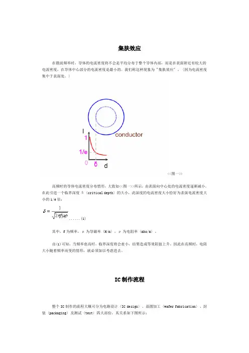
集肤效应在微波频率时,导体的电流密度将不会是平均分布于整个导体内部,而是在表面附近有较大的电流密度,在导体中心部分的电流密度是最小的。
我们称这种现象为〝集肤效应〞。
〈因为电流密度集中于表面处。
〉<<图一>>高频时的导体电流密度分布情形,大致如<<图一>>所示,由表面向中心处的电流密度逐渐减小。
在此引进一个临界深度δ〈critical depth〉的大小,此深度的电流密度大小恰好为表面电流密度大小的1/e倍: (1)其中,f为频率,μ为导磁率〈H/m〉,ρ为电阻率〈mho/m〉。
由(1)可知,当频率愈高时,临界深度将会愈小,结果造成等效阻值上升。
因此在高频时,电阻大小随着频率而变的情形,就必须加以考虑进去。
IC制作流程整个IC制作的流程大概可分为电路设计〈IC design〉、晶圆加工〈wafer fabrication〉、封装〈packaging〉及测试〈test〉四大部份,其关系如下图所示:当我们决定好对一个IC所要求的功能及其工作规格后,便开始着手电路设计。
电路设计的主要目的在产生布局图〈layout〉,它能定义出晶圆加工制程中所需要的各层图案〈pattern〉。
藉由布局图,可做成晶圆加工制程中所需要的各道光罩〈mask or reticle〉。
接下来的晶圆加工制程,可以说是整个IC制作流程中最复杂、资金及技术最密集的一部份。
这个部份就是要将上一个设计程序所设计出来的电路及电子组件,能在晶圆上加以实现。
而电路上所用到的电子组件〈晶体管、电阻、电容、电感...〉及其间的联机〈interconnection〉,则必须靠各单元制程〈氧化、黄光微影、薄膜沉积、蚀刻、参杂...〉间的反复配合才能完成。
光罩在此的功用在于能定义出各层薄膜的图案、组件区域,或组件间的联机情形,以达所要的电路功能及规格。
所谓的〝晶圆代工〞厂,就是专门将别家公司所设计出的电路,以该公司晶圆加工制造厂〈Fab.〉现有的技术能力及仪器设备,完成其晶圆加工制程之意。
太阳能电池专业英语
A1.中文:暗饱和电流英文:Dark Saturation Current解释:没有光照的条件下,将PN结反偏达到饱和时的电流。
降低暗饱和电流利于提高电池品质在以下的理想二极管公式中,I =流过二极管的总电流; I0 = “暗饱和电流”, V = 加在二极管两端的电压B1.中文:包装密度英文:Packing density解释:组件中被太阳能电池覆盖的面积对比于整个组件的面积。
它影响了组件的输出功率及工作温度2.中文:背电场英文:Back Surface Field解释:在电池背面由于重掺杂引起的电场。
该电场会排斥少数载流子以使它们远离高复合率的背表面3.中文:背面反射/底面反射英文:Rear Surface Reflection解释:穿过电池而未被吸收的长波光会被电池背面的金属或染料反射回电池,增大吸收概率4.中文:本底掺杂英文:Background Doping解释:电池衬底的掺杂浓度5.中文:表面制绒英文:Surface Texturing解释:用物理或化学的方法将平滑的硅电池表面变得粗糙,增大光捕获,减小反射6.中文:并网系统英文:Grid-connected Systems解释:并网系统指由光伏组件供电的,接入公用电网的光伏系统。
这类系统无须蓄电池7.中文:薄膜太阳能电池英文:Thin-film Solar Cells解释:薄膜太阳能电池是通过在衬底上镀光伏材料薄层制成的,厚度从几微米到几十微米不等。
成本较低但效率普遍较低8.中文:复合英文:Recommbination解释:又称为载流子复合,是指半导体中的载流子(电子和空穴)成对消失的过程。
9.中文:表面复合速率英文:Surface Recombination Velocity解释:当少子在表面消失时,由于浓度梯度,少子会从电池体流向表面。
表面复合速度表征表面复合的强弱。
C1.中文:掺杂英文:Doping解释:在本征半导体里加入施主或受主杂质(通常是磷或硼)使半导体内自由载流子浓度变高并使其具有p型或n型半导体的性质2.中文:串联电阻英文:Series Resistance解释:由电池体、电极接触等产生的分压电阻。
半导体器件中英名词解释
built-in electric field: An electric field due to the separation of positive and negative space charge densities in the depletion region.
increase, showing breakdown, called tunneling breakdown, also known as Zener breakdown.
隧道击穿/齐纳击穿: 对重掺杂pn结, 随着反偏电压增大, 可能使p区价带顶高于n区导带底, p区价带的电子可以通过隧道效应直接穿过禁带到达n区导带, 成为导带载流子。 当结上反偏 电压增大到一定程度,将使隧穿电流急剧增加,呈现击穿现象,称为隧道击穿,又称为齐纳 击穿。
critical electric field: The peak electric field in the space charge region at breakdown.
临界电场:发生击穿时pn结空间电荷区的最大电场强度。
varactor diode: A diode whose reactance can be varied in a controlled manner with bias voltage.
abrupt junction approximation: The assumption that there is an abrupt discontinuity in space charge density between the space charge region and the neutral semiconductor region.
金红石型二氧化钛的价带电子结构表征(110)-(1 - 2)
Valence band electronic structure characterization of the rutile TiO 2(110)-(1×2)reconstructed surfaceC.Sánchez-Sánchez a ,b ,M.G.Garnier c ,P.Aebi c ,M.Blanco-Rey d ,P.L.de Andres a ,d ,J.A.Martín-Gago a ,e ,M.F.López a ,⁎aInstituto Ciencia de Materiales de Madrid (ICMM-CSIC),C/Sor Juana Inés de la Cruz 3,28049-Madrid,Spain bInstituto de Ciencia de Materiales de Sevilla (ICMSE-CSIC),Américo Vespucio 49,41092-Sevilla,Spain cDépartement de Physique and Fribourg Center for Nanomaterials,Universitéde Fribourg,CH-1700Fribourg,Switzerland dDonostia International Physics Center,Universidad del País Vasco UPV/EHU,Paseo Manuel de Lardizábal 4,20018Donostia-San Sebastián,Spain eCentro de Astrobiologia (CSIC-INTA),28850Madrid,Spaina b s t r a c ta r t i c l e i n f o Article history:Received 31May 2012Accepted 28September 2012Available online 6October 2012Keywords:Titanium oxideElectronic structure ARUPS DefectsThe electronic structure of the TiO 2(110)-(1×2)surface has been studied by means of angular resolved ultraviolet photoemission spectroscopy (ARUPS).The valence band dispersion along the high symmetry sur-face directions,[001]and [1–10],has been recorded.The experimental data show no dispersion of the band-gap Ti 3d states.However,the existence of dispersive bands along the [001]direction located at about 7eV below the Fermi level is reported.The existence of two different contributions in the emission from the defects-related state located in the gap of the surface is univocally shown for the first time.©2012Elsevier B.V.All rights reserved.1.IntroductionMetal oxides are of great importance due to their use in several technological applications such as heterogeneous catalysis,photo-chemistry,sensors,and composite materials [1].Among all of them,titanium dioxide has become the prototype for surface science studies due to its ordered structure and its capability of conduction upon re-duction.One of the main areas of application of TiO 2is the field of ca-talysis,being nowadays one of the more widely used materials for catalytic supports.In order to better understand and improve its cat-alytic properties,a detailed knowledge of its electronic structure is of crucial importance.The rutile TiO 2(110)is the most stable face and,in this work,we shall focus on its electronic properties.This surface,upon sputtering and annealing under ultra-high vacuum (UHV)con-ditions,presents the well-known (1×1)structure corresponding to the bulk truncated structure,modi fied by simple but relevant surface relaxations [2].The stable (1×1)surface transforms into a long range ordered structure with (1×2)symmetry upon further reduction of the sub-strate [3].The quality of this new surface depends on the reduction level of the TiO 2crystal,on the annealing temperature achieved dur-ing sample preparation,and on the duration of the annealing.This surface reconstruction has been the subject of many investigations during the last years.Most of the scienti fic efforts have been devotedtowards the determination of the geometrical disposition of atoms.This has been a matter of controversy,as several atomic models have been proposed based on different experimental techniques and theoretical calculations [4–9].In a previous work carried out by our group,the (1×2)structure was elucidated from density functional theory (DFT)calculations and quantitative low-energy electron diffraction experiments [LEED-I(V)][10,11].Similar to Onishi's proposal,a Ti 2O 3stoichiometry on the sur-face was favored,although some structural differences between these two models were reported.Surprisingly,not many investigations have focused on the electronic structure of the (1×2)surface reconstruction.One signi ficant issue in the study of TiO 2is the presence of defects of different nature,which are typical of this kind of substrates.Its importance arises from the fact that the presence of these defects,hy-droxyl impurities,oxygen atom vacancies and interstitials Ti atoms,confer unusual properties to this material.The local character of these defects makes near-field scanning probe microscopy a crucial technique for their study,although its assignation is not always clear and straightforward [12–18],not only regarding the surface to-pography but also from the electronic point of view.Depending on the amount of defects,some can be also detectable by spectroscopic techniques.The oxidation state of titanium cations in stoichiometric (110)TiO 2corresponds nominally to Ti 4+.However,an important contribution of defects will be originated when the surface is reduced by annealing and/or ion bombardment.The presence of these defects,not only mainly oxygen vacancies but also,in a lower amount,inter-stitials Ti 3+atoms,on the TiO 2(110)surface will lead to an excess ofSurface Science 608(2013)92–96⁎Corresponding author.Tel.:+34913349081;fax:+34913720623.E-mail address:m flopez@icmm.csic.es (M.F.López).0039-6028/$–see front matter ©2012Elsevier B.V.All rights reserved./10.1016/j.susc.2012.09.019Contents lists available at SciVerse ScienceDirectSurface Sciencej o u r na l h o me p a g e :ww w.e l s e v i e r.c o m /l o c a t e /s u s celectrons at these specific sites.This residual charge is expected to be transferred to the Ti atoms located close to defects[19–21].Consequently,the trapped electron will partially populate the Ti3d orbitals and will change the oxidation state of the adjacent Ti cations from4+to3+.For this reason,when the defects contribu-tion is high,a new electronic state appears in the gap region below EF. This state is referred in ultraviolet photoemission spectra as band-gap or defects-related state and it has been the subject of many spec-troscopic studies[22,23].Since the TiO2(110)-(1×2)surface recon-struction is obtained from the(1×1)surface by annealing at high temperature,a significant amount of defects are originated in this process.Thus,a clear enhancement of the Ti3+band-gap state is expected for the(1×2)reconstruction[24].Additionally,the presence of surface Ti2O3rows where the Ti cations have a nominal 3+oxidation state will contribute to enhance the emission at the band-gap state.In this paper,the valence band electronic structure of the rutile TiO2(110)-(1×2)surface is investigated by angular resolved ultra-violet photoemission spectroscopy(ARUPS).Special effort has been made to understand the origin of the band-gap state that appears at a binding energy(BE)of approximately0.9eV.We will show that for the(1×2)reconstruction this peak presents a double contribution, one associated to the Ti3+in the Ti2O3rows of the(1×2)reconstruc-tion,and a different one related to the defective Ti3+atoms present throughout the crystal bulk.We also report the presence of a disper-sive band at a BE of about7eV and k//=0.35Å−1.2.Material and methodsExperiments have been carried out in two different ultra-high vacu-um(UHV)chambers,both of them with a base pressure better than 1·10−10mbar.In both cases,a commercial rutile TiO2(110)sample (Mateck)was prepared through repeated cycles of sputtering and annealing at1150K until a sharp(1×1)or(1×2)LEED pattern was obtained.The(1×1)surface is characteristic of a stoichiometric sample or a poorly reduced bulk,while the(1×2)reconstruction is typical of heavily reduced substrates.For the UPS band-gap peak study,three dif-ferent substrates were considered:low,medium and heavily reduced. The criteria used to discern among these three cases have been the color of the sample and the surface structure.In this way,for example, low reduced sample presents a light blue color and a(1×1)surface structure(as observed by STM and LEED).Medium reduced sample is dark blue but still with a(1×1)surface structure.Finally,heavily re-duced sample is almost black and presents a(1×2)surface termination. In all cases the same sample was used,and the degree of reduction was increased by controlling the annealing temperature and the cycle dura-tion.ARUPS measurements were performed using monochromatized He-I radiation from a He discharge lamp in combination with a VG EscaLab Mk II photoelectron spectrometer(20meV resolution),and a sample goniometer for full hemispherical Angular Resolved Photoemis-sion Spectroscopy(ARPES)[25].The angular acceptance and resolution is1°full-cone.Therefore,this corresponds to an approximate kII inte-gration of the Brillouin zone of less than0.04Å−1.Measurements of the band-gap state were done at the UHV chamber located at Centro de Astrobiología(CSIC-INTA),equipped with a hemispherical electron analyzer and a He-I lamp.To perform the ultraviolet photoemission spectroscopy(UPS)analysis the spectra werefitted to a least squares combination of Gaussian components.The background selected for thefitting procedure of the UPS spectra was a linear one as it is the typ-ical used for inelastic backgrounds without a stepwise change in inten-sity,as it was our case.All spectra were recorded at room temperature.The(1×2)reconstructed Ti2O3surface structure was determined from DFT and dynamical LEED in a previous work[10],and the surface model in the present paper has been constructed accordingly.The (1×2)supercell lattice dimensions are a=13.22Å,b=2.99Å,and c=3a,containing a slab of70atoms mirror-symmetric about its middle plane,exposing the Ti2O3reconstruction at both sides(see supplementary information).This ensures that the electronic struc-ture features come only from the bulk and the(1×2)reconstructed surface.The TiO2bulk unit cell dimensions are a=b=4.68Åand c=2.99Å.The plane wave basis has been constructed with a cut-off energy of400eV and a Monkhorst-Pack k-point mesh of7×13×1 (4×4×7for bulk)[26].Energy was converged up to0.01meV/ion and the Fermi level to0.001meV/ion.The supercell height,c,is such that the solid occupies approximately one half of the supercell, which we have shown to be enough to avoid interactions between consecutive slabs.The slab thickness is such that Mulliken charges of atoms in the central Ti–O layer are in good agreement with those of the bulk.The outmost19atoms of both sides of the slab were allowed to relax further with tolerances of0.05eV/Åin the force per atom and 0.001Åin the displacement.Thefinal atomic coordinates differed from those of the previous work[10]by no more than0.04Å.Actual calculations have been performed with the CASTEP code[29].3.Results and discussionFig.1(a)shows a schematic representation of the atomic arrange-ment corresponding to the rutile TiO2(110)-(1×2)surface recon-struction,as derived from previous LEED I(V)and DFT calculations [10].The most protruding features on this surface are the Ti2O3 rows,which extend along the[001]rge gray and small red circles correspond to Ti and O atoms,respectively.Ti3+atoms as-sociated to the surface reconstruction are marked by arrows.The red rectangle of Fig.1(b)represents the surface Brillouin zone(SBZ)for the TiO2(110)-(1×2)termination,with the two high-symmetry di-rections indicated.In this representation also the SBZ for the TiO2 (110)-(1×1)surface is exhibited as a black rectangle.As it can be ob-served,both the(1×1)and the(1×2)surfaces present a rectangular structure in the reciprocal space.Fig.2(a)and(b)exhibits bidimensional representations of the experimental ARUPS spectra corresponding to the rutile TiO2(110)-(1×2)valence band as a function of the momentum parallel compo-nent k II along[001]and[1–10]directions,respectively.In both graphs,the high symmetry points of the SBZ as well as the Fermi sur-face edge are indicated.In the images,the darkest features corre-spond to more intense photoemission peaks while the brightest ones represent the less intense emissions.Along the[001]direction, i.e.the direction of the Ti2O3rows,a convex dispersive band located at a binding energy of about7eV and centered at0.35Å−1can be ob-served.On the other hand,no dispersion is observed along the[1–10] direction,i.e.perpendicular to the reconstruction rows.Previous re-sults on TiO2(110)-(1×1)showed weak dispersion of the states cor-responding to the valence band[27].Fig.2(c)and(d)shows the bidimensional representations of the experimental band-gap state ARUPS spectra along the two high sym-metry directions,[001]and[1–10],respectively.The data indicate that no dispersion can be distinguished by ARUPS.In particular,from Fig.2(c),we conclude there is no significative experimental dispersion of the band-gap state of the(1×2)surface along the direction of the Ti2O3surface wires.This result contrasts with the theoretical pre-diction derived from DFT calculations about the metallic character of the Ti2O3chains along the[001]direction[10].This discrepancy has been associated to the tendency of the GGA functional[30]to overestimate the delocalization of states that may be otherwise local-ized by different factors,like correlation effects and the quasi-1D char-acter of states running along the reconstruction chains.Indeed,the use of GGA+U as an alternative exchange and correlation functional fa-vors the opening of a gap along the[001]direction and results in a dis-persive state in the band gap,localized at the subsurface Ti atoms in the trenches between the Ti2O3chains[31,32].Fig.3shows the com-puted valence band electronic structure for a slab(left)and the corre-sponding projection of bulk states along the GΓ–Z direction(right).93C.Sánchez-Sánchez et al./Surface Science608(2013)92–96Blue dots label states with more than an 80%contribution from atoms of the Ti 2O 3chains,while green dots represent the same for atoms lo-cated on the TiO 2tri-layer closest to the surface.As it is well known,DFT underestimates the band gap because correlation effects are only taken into account in an approximate way (we obtain for bulk TiO 2a band gap of 2eV).Furthermore,the Hohenberg –Kohn theorem applies strictly speaking only to the ground state,and excited states,e.g.in the conduction band,are only covered in an approximate,perturbative way.Finally,the ARUPS technique only provides infor-mation about the valence band.Therefore,we only attempt to com-pare the experimental and theoretical valence bands.In the right hand side panel of Fig.3we show the bands along the G –Z direction from a bulk only calculation (i.e.from the 1×1×1bulk unit cell for TiO 2,as described above).We compare the bulk states from this calcu-lation with the experimental ones in Fig.2a.It is interesting to notice that these states are not affected by the low-dimensional comments made above for the Ti 2O 3chains,and are therefore properly described by a GGA functional.This point is double-checked by performing LDA+U calculations (U=4.5eV);the main effect is a rigid shift of bands by about half an eV to higher binding energies,but no notice-able distortions.The main observed features appear above and below 7eV,similarly as can be seen in the experiment (panel (a)in Fig.2).On the other hand,the states related to the surface (green tri-angles and circles)show a remarkable lack of dispersion very near 7eV.The experimental resolution does not allow seeing this flat surface-like band.For the experimental band structure,a dispersive band similar to the theoretical one happens above and below 7eV,as seen by comparing with Fig.2(panel a).Finally,we notice in Fig.2(c)and (d),that the data exhibit inten-sity maxima at approximately 0.8Å−1(along [001])and 0.15Å−1(along [1–10]).This can be explained by final-state scattering effects,i.e.as an ultraviolet photoelectron diffraction effect (UPD)[28].In order to extract additional information on the band-gap states,UPS measurements for three different reduction levels of the sub-strate have been performed.As it has been mentioned above,it is known that the band-gap state is related to Ti 3+states and it appears after bulk reduction.However,in the case of the (1×2)surface recon-struction,there are also Ti 3+states associated to the Ti 2O 3rows oftheFig.1.a)Schematic representation of the atomic arrangement corresponding to the (1×2)TiO 2(110)surface reconstruction as inferred from DFT calculations (only the last layers are shown).Large (blue)and small circles (red)correspond to Ti and O atoms,respectively.b)Surface Brillouin zone for the TiO 2(110)-(1×2)surface reconstruction marked in red with the two high-symmetry directions [001]and [1–10].The black rectangle corresponds to the extended SBZ for TiO 2(110)-(1×1)surface.Fig.2.Bidimensional representation of the ARUPS spectra of the TiO 2(110)-(1×2)surface as a function of k II along (a)[001]and (b)[1–10]directions for the valence band region,and (c)and (d)for the band-gap states region along [001]and [1–10],respectively.94 C.Sánchez-Sánchez et al./Surface Science 608(2013)92–96surface reconstruction.It is generally accepted that the exact binding energy of an electron depends not only on the level from which pho-toemission originates but also on the oxidation state of the atom and the local chemical environment.Thus,modi fications on the local chemical environment introduce small shifts in the peak position,which are known as chemical shifts.In the present case,two different chemical environments for the Ti 3+ions are present,one at the bulk and another at the Ti 2O 3surface rows.For this reason,these two dif-ferent chemical settings should give rise to different photoemission signals separated by a certain binding energy,making possible their distinction by means of UPS.Fig.4exhibits UPS spectra of the band-gap state region for both a poorly reduced and a highly reduced substrate with a (1×1)surface symmetry,and for a heavily reduced substrate with (1×2)symmetry at the surface.In all spectra,the red solid line through the black data circles represents the result of the least-squares fit,with the blue dashed-dotted component giving the signal corresponding to the low binding energy (BE)peak and the green solid curve showing the high BE emission.The yellow dashed line represents the linear background.As it can be observed in Fig.4(a),for a low reduction level associated to a TiO 2(110)-(1×1)surface,just one peak is needed in order to properly fit the ex-perimental data (chi-square test is 0.079).The binding energy for this peak is 0.78eV with a FWHM value of 0.62eV.If the reduction level isincreased (but still preserving a (1×1)surface)an enhancement of the band-gap state is observed,as it is evident from Fig.4(b).Again,only one peak is necessary to fit the experimental data,being this peak almost identical to the previous one,except for an increase in its intensity.In this case,its binding energy is 0.77eV and the FWHM is 0.63eV (chi-square 0.047).On the other hand,upon further reduction of the substrate a phase transition takes place at the surface,where a new reconstruction appears as it is evidenced from LEED and STM measurements.This new reconstruction,characterized by a Ti 2O 3surface stoichiometry,presents a wider and asymmetric band-gap state peak,which makes necessary the addition of a second com-ponent in the fit.Indeed,for the heavily reduced substrate with a (1×2)surface termination,two contributions have been required to properly fit the band-gap state emission,one located at the same posi-tion as in the previous cases,and another one located at a slightly higher BE (Fig.4(c)).The two curves used in these fits are located at 0.75eV and 1.18eV BE showing a FWHM of 0.67eV and 0.51eV,re-spectively (chi-square 0.077).Attempts to fit this spectrum with a sin-gle component have been unsuccessful due to the asymmetry of the experimental data (best chi-square obtained has been 0.43).This new state appearing together with the (1×2)surface reconstruction and not observed for any of the (1×1)symmetry cases,can only be associated to the Ti 3+states of the Ti 2O 3rows.As it would be expected from the existence of two different chemical environments associat-ed with the Ti 3+states,the UPS experiments clearly indicate the pres-ence of two different contributions in the band-gap state peak:one component is related to the bulk defects typical of the (1×1)structureFig.3.Ab-initio DFT electronic structure calculation along the [001]direction (G –Z).(i)Left panel:band structure of the slab supercell (with the Ti 2O 31×2reconstructed chains).(ii)Right panel:band structure of the 1×1×1bulk TiO 2unit cell projected along the G –Z direction.Red regions in the graph correspond to bulk states with a large weight in the projection along the G –Z direction.Blue and violet correspond to states with small weight and black regions are either gaps or zones with a very small number of states.Green triangles label electronic states that have more than 80%con-tribution from atoms in the Ti 2O 3group,as obtained in the left panel.Green circles label the same corresponding to atoms of the topmost trilayer (TiO 2).Green ellipse marks the dispersive band similar to the experimentalone.Fig.4.UPS spectra of the band-gap states region for:(a)poorly reduced substrate with a (1×1)surface,(b)highly reduced substrate with (1×1)symmetry at the surface,and (c)heavily reduced substrate with a (1×2)symmetry at the surface.95C.Sánchez-Sánchez et al./Surface Science 608(2013)92–96(low BE peak),and the other is due to the Ti atoms present at the sur-face reconstruction in the(1×2)surface(high BE peak).The presence of this new surface termination in the(1×2)TiO2(110)sample sur-face,i.e.the Ti2O3surface rows,is the origin of the sudden appearance of the latter component.It is important to note the increase in the in-tensity of the peak at0.75eV for this sample in comparison to the less reduced ones.The reason of this effect is the increasing amount of Ti3+states not only at the Ti2O3surface rows(peak at1.18eV BE) but also at the bulk(peak at0.75eV BE)when the sample has been reduced.It is worthy to comment on the different contexts for Ti3+and Ti4+ atoms in the(1×2)TiO2(110)sample.The geometrical disposition of the Ti3+atoms at the surface within the Ti2O3chains,and therefore its chemical environment,is completely different to that of the of Ti3+ atoms at the bulk near the defect sites.However,in the case of the Ti4+atoms,the geometrical arrangement in both cases,bulk and surface,is the same.For this reason,no shift in the binding energies should be expected for the surface Ti4+atoms.The possibility of discerning the two components for the band-gap states peak leads to some important consequences.For example,this method based onfitting the bad-gap states region can be used to con-firm the existence and quality level of the(1×2)surface reconstruc-tion on TiO2(110).It could be also used to determine the nature of the interaction of a molecular adsorbate on the(1×2)reconstruction by analyzing the evolution of the relative intensity of the different com-ponents of the band-gap state peak upon deposition.4.ConclusionsIn this paper,the electronic structure of the rutile TiO2(110)-(1×2)surface reconstruction has been characterized,paying special attention to Ti3+related band-gap state.By means of ARUPS,the presence of a downward dispersive band along the rutile TiO2(110)-(1×2)[001]surface direction is determined.This band,with its max-imum at0.35Å−1,appears7eV below the Fermi edge.No dispersion of the band-gap states is observed by ARUPS.Regarding the band-gap states emission,the double nature of this peak has been identified. One component is associated to the Ti3+cations next to the bulk de-fects and the other,observed for the case of the TiO2(110)-(1×2)sur-face reconstruction,to the Ti3+cations in the Ti2O3chains present at the surface.AcknowledgmentsThis work has been supported by the Spanish CYCIT(MAT2011-26534)and the Ministry of Science and Innovation(CSD2007-41 NANOSELECT).C.S.S.gratefully acknowledges Ministerio de Educación for thefinancial support inside the“FPU programme”under the AP2005-0433grant.M.G.G.and P.A.are grateful for the support by the Fonds National Suisse pour la Recherche Scientifique through Div. II and the Swiss National Center of Competence in Research MaNEP. M.B.-R.acknowledgesfinancial support from the Gipuzkoako Foru Aldundia and the European Union7th Framework Programme(FP7/ 2007–2013)under grant agreement no.FP7-PEOPLE-2010-RG276921. Appendix A.Supplementary dataSupplementary data to this article can be found online at http:// /10.1016/j.susc.2012.09.019.References[1]U.Diebold,Surf.Sci.Rep.48(2003)53.[2]W.Busayaporn,X.Torrelles,A.Wander,S.Tomić,A.Ernst,B.Montanari,N.M.Harrison,O.Bikondoa,I.Joumard,J.Zegenhagen,G.Cabailh,G.Thornton,R.Lindsay,Phys.Rev.B81(2010)153404(and references therein).[3]J.Abad,C.Rogero,J.Méndez,M.F.López,J.A.Martín-Gago,E.Román,Surf.Sci.600(2006)2696.[4]P.J.Møller,M.C.Wu,Surf.Sci.224(1989)265.[5]H.Onishi,K.I.Fukui,Y.Iwasawa,Bull.Chem.Soc.Jpn.68(1995)2447.[6] C.L.Pang,S.A.Haycock,H.Raza,P.W.Murray,G.Thornton,O.Gülseren,R.James,D.W.Bullet,Phys.Rev.B58(1998)1586.[7]R.A.Bennett,P.Stone,N.J.Price,M.Bowker,Phys.Rev.Lett.82(1999)3831.[8]K.T.Park,M.H.Pan,V.Meunier,E.W.Plummer,Phys.Rev.Lett.96(2006)226105.[9]N.Shibata,A.Goto,S.-Y.Choi,T.Mizoguchi,S.D.Findlay,T.Yamamoto,Y.Ikuhara,Science322(2008)570.[10]M.Blanco-Rey,J.Abad,C.Rogero,J.Mendez,M.F.Lopez,J.A.Martin-Gago,P.L.deAndres,Phys.Rev.Lett.96(2006)055502.[11]M.Blanco-Rey,J.Abad, C.Rogero,J.Méndez,M.F.López, E.Román,J.A.Martín-Gago,P.L.de Andrés,Phys.Rev.B75(2007)081402(R).[12]uritsen,A.S.Foster,G.H.Olesen,M.C.Christensen,A.Kühnle,S.Helveg,J.R.Rostrup-Nielsen,B.S.Clausen,M.Reichling,F.Besenbacher,Nanotechnology 17(2006)3436.[13]X.Cui,Z.Wang,S.Tan,B.Wang,J.Yang,J.G.Hou,J.Phys.Chem.C113(2009)13204.[14] C.L.Pang,O.Bikondoa,D.S.Humphrey,A.C.Papageorgiou,G.Cabailh,R.Ithnin,Q.Chen,C.A.Muryn,H.Onishi,G.Thornton,Nanotechnology17(2006)5397. [15] C.Sánchez-Sánchez, C.González,P.Jelinek,J.Méndez,P.L.de Andrés,J.A.Martín-Gago,M.F.López,Nanotechnology21(2010)405702.[16] A.Yurtsever,Y.Sugimoto,M.Abe,S.Morita,Nanotechnology21(2010)165702.[17]R.Bechstein,C.González,J.Schütte,P.Jelínek,R.Pérez,A.Kühnle,Nanotechnology20(2009)505703.[18]H.P.Pinto,G.H.Enevoldsen,F.Besenbacher,uritsen,A.S.Foster,Nanotech-nology20(2009)264020.[19]P.Krüger,S.Bourgeois,B.Domenichini,H.Magnan,D.Chandesris,P.Le Fèvre,A.M.Flank,J.Jupille,L.Floreano,A.Cossaro,A.Verdini,A.Morgante,Phys.Rev.Lett.100(2008)055501.[20]M.Nolan,S.D.Elliott,J.S.Mulley,R.A.Bennett,M.Basham,P.Mulheran,Phys.Rev.B77(2008)235424.[21]M.V.Ganduglia-Pirovano,A.Hofmann,J.Sauer,Surf.Sci.Rep.62(2007)219.[22]R.Patel,Q.Guo,I.Coks,E.M.Williams,E.Roman,J.L.de Segovia,J.Vac.Sci.Technol.A15(1997)2553.[23]Z.Zhang,S.Jeng,V.E.Henrich,Phys.Rev.B43(1991)12004.[24]J.Abad,C.Rogero,J.Méndez,M.F.López,J.A.Martín-Gago,E.Román,Appl.Surf.Sci.234(2004)497.[25]T.Pillo,L.Patthey, E.Boschung,J.Hayoz,P.Aebi,L.Schlapbach,J.ElectronSpectrosc.Relat.Phenom.97(1998)243.[26]H.J.Monkhorst,J.D.Pack,Phys.Rev.B13(1976)5188.[27]S.Fischer,J.A.Martín-Gago,E.Román,K.D.Schierbaum,J.L.de Segovia,J.ElectronSpectrosc.Relat.Phenom.83(1997)217.[28]J.Osterwalder,T.Greber,P.Aebi,R.Fasel,L.Schlapbach,Phys.Rev.B53(1996)10209.[29]S.Clark,M.Segall,C.Pickard,P.Hasnip,M.Probert,K.Refson,M.C.Payne,Z.Kristallogr.220(2005)570().[30]J.P.Perdew,K.Burke,M.Ernzerhof,Phys.Rev.Lett.77(1996)3865.[31]V.Celik,H.Unal,E.Mete,S.Ellialtioglu,Phys.Rev.B82(2010)205113.[32]H.Unal,E.Mete,S.Ellialtioglu,Phys.Rev.B84(2011)115407.96 C.Sánchez-Sánchez et al./Surface Science608(2013)92–96。
cbm和vbm电荷计算
cbm和vbm电荷计算English Answer:CBM and VBM charge calculation.The charge of the conduction band minimum (CBM) and valence band maximum (VBM) is an important parameter for understanding the electronic properties of semiconductors. It can be used to calculate the band gap, the effective mass of electrons and holes, and the carrier concentration.There are two main methods for calculating the charge of the CBM and VBM:The density functional theory (DFT) method: This method uses a first-principles approach to calculate the electronic structure of a semiconductor. It is based on the Hohenberg-Kohn theorem, which states that the ground state energy of a system is a unique functional of the electron density. The DFT method can be used to calculate the chargeof the CBM and VBM by solving the Kohn-Sham equations.The empirical tight-binding (ETB) method: This method uses a simplified model of the electronic structure of a semiconductor. It is based on the assumption that the electrons are localized on the atoms of the semiconductor. The ETB method can be used to calculate the charge of the CBM and VBM by solving the secular equation.The DFT method is more accurate than the ETB method, but it is also more computationally expensive. The ETB method is less accurate than the DFT method, but it is also less computationally expensive.The choice of method for calculating the charge of the CBM and VBM depends on the accuracy and computational cost requirements of the application.Here are some additional details about the DFT and ETB methods:The DFT method is based on the Hohenberg-Kohn theorem,which states that the ground state energy of a system is a unique functional of the electron density. The DFT method solves the Kohn-Sham equations, which are a set of self-consistent equations that can be used to calculate the electron density and the ground state energy. The DFT method can be used to calculate the charge of the CBM and VBM by calculating the electron density at the CBM and VBM.The ETB method is based on the assumption that the electrons are localized on the atoms of the semiconductor. The ETB method solves the secular equation, which is a matrix equation that can be used to calculate the energy levels of the electrons. The ETB method can be used to calculate the charge of the CBM and VBM by calculating the energy levels of the electrons at the CBM and VBM.The DFT method is more accurate than the ETB method, but it is also more computationally expensive. The ETB method is less accurate than the DFT method, but it is also less computationally expensive.The choice of method for calculating the charge of theCBM and VBM depends on the accuracy and computational cost requirements of the application.Chinese Answer:CBM 和 VBM 电荷计算。
k.p方法计算应变量子阱空穴能级[整理版]
Spin-orbit-coupling effects on the valence-band structure of strained semiconductor quantum wellsCalvin Yi-Ping Chao and Shun Lien ChuangDepartment of Electrical and Computer Engineering, University of Illinois摘要:找到一组将6×6 Luttinger-Kohn 哈密顿量对角化为两个3×3块的酉变换,使得计算量子阱能带时更有效。
使用这些公式,系统的研究了应变量子阱中重空穴、轻空穴和自旋轨道分裂耦合。
给出应变对k空间能量表面的影响,给出包含与不包含自旋轨道分裂能带的结果。
结果显示,自旋轨道分裂耦合对能带特别是高应变量子阱能态影响很明显,不能忽略。
1.简介应变可以是调整半导体能带参数的有力工具,在量子阱激光器,调制器,探测器等中有重要的应用。
例如对于应变量子阱激光器,应变使得量子阱价带带边在k=0处分裂,降低平面有效质量,从而降低态密度,降低阈值电流。
各向同性(静水力学的)应变改变带隙,各向异性(单轴或切应变)使得价带在k=0处简并分离。
应变导致重空穴、轻空穴、自旋轨道分裂带额外的耦合,这些耦合在非应变量子阱计算中通常被忽略,但对于高应变量子阱,忽略这些耦合将导致计算能级误差几十个meV,有效质量误差高于30%。
本文的目的就是证明应变如何影响半导体价带能级,着重于重空穴、轻空穴、自旋轨道分裂带额外的耦合。
使用的公式基于Luttinger-Kohn 哈密顿量和包络函数近似。
以下第二部分研究应变体材料带边能量公式和有效质量。
第三部分结合应变和量子效应,集中讨论应变量子阱的能级计算,在轴近似下,得到一组将6×6 Luttinger-Kohn 哈密顿量对角化为两个3×3块的酉变换,由这简单的哈密顿量,可以计算应变量子阱的能级。
- 1、下载文档前请自行甄别文档内容的完整性,平台不提供额外的编辑、内容补充、找答案等附加服务。
- 2、"仅部分预览"的文档,不可在线预览部分如存在完整性等问题,可反馈申请退款(可完整预览的文档不适用该条件!)。
- 3、如文档侵犯您的权益,请联系客服反馈,我们会尽快为您处理(人工客服工作时间:9:00-18:30)。
Home Search Collections Journals About Contact us My IOPscienceValence band electronic structure of Pr1−x Sr x MnO3 from photoemission studiesThis content has been downloaded from IOPscience. Please scroll down to see the full text.2005 J. Phys.: Condens. Matter 17 2993(/0953-8984/17/19/013)View the table of contents for this issue, or go to the journal homepage for moreDownload details:IP Address: 202.206.97.174This content was downloaded on 01/04/2016 at 03:09Please note that terms and conditions apply.I NSTITUTE OF P HYSICS P UBLISHING J OURNAL OF P HYSICS:C ONDENSED M ATTER J.Phys.:Condens.Matter17(2005)2993–2999doi:10.1088/0953-8984/17/19/013Valence band electronic structure of Pr1−x Sr x MnO3 from photoemission studiesP Pal1,M K Dalai1,B R Sekhar1,S N Jha2,S V N Bhaskara Rao2,N C Das2,C Martin3and F Studer31Institute of Physics,Sachivalaya Marg,Bhubaneswar,India2Spectroscopy Beamline,INDUS-I,Centre for Advanced Technology,Indore-452013,India3Laboratoire CRISMAT,UMR6508,ISMRA,Boulevard du Marechal Juin,14050Caen,FranceE-mail:sekhar@iopb.res.inReceived18December2004,infinal form15March2005Published29April2005Online at /JPhysCM/17/2993AbstractWe have studied the charge carrier doping dependent changes in the valenceband electronic structure of the Pr1−x Sr x MnO3system across the orbital orderedcompositions using ultraviolet photoelectron spectroscopy.The d x2−y2orbitalordering is found to be causing an enhancement of the Mn3d–O2p hybridizationstrength and thereby the Mn3d contribution to the subbands in the valenceregion.Our photoemission studies using different photon energies help inelucidating the nature and composition of the valence band features.1.IntroductionThe electronic structure of manganites with general composition RE1−x A x MnO3(RE=rare earth,A=alkaline earth)exhibiting colossal magnetoresistance(CMR)properties has been afield of immense interest since their discovery[1,2].Properly doped compounds of this Mn3+/Mn4+mixed valent system show a ferromagnetic metallic behaviour at low temperatures and a paramagnetic insulating behaviour at high temperatures.The temperature and dopingdependent metal–insulator transitions in these materials are found to be closely related to the unique electronic structure derived from the Mn3d and O2p hybridized orbitals[3].The 3d orbitals of Mn in the MnO6octahedra,which are split by the crystalfield into low-lying t2g and e g states,are further split by the Jahn–Teller distortion.The double-exchange(DE) model[4–6]says that the itinerant,doped charge carriers(Mn4+species or e g holes)mediate between the localized t2g spins and cause the increase in the mobility of the charge carriers. However,recent progress in experimental and theoretical work has brought the realization that the DE model is insufficient to explain all the properties of these CMR materials[7–10], particularly the high-resistivity behaviour above the transition temperature T c[11].Undoped parent compounds of these materials,like LaMnO3and PrMnO3(so-called A-type antiferromagnetic(AFM)insulators),show a strong interplay between spin and orbital 0953-8984/05/192993+07$30.00©2005IOP Publishing Ltd Printed in the UK29932994P Pal et al ordering originating from the single occupancy of the doubly degenerate e g orbitals of Mn3+ ions.With charge carrier doping at the A-site,many of them show well defined orbital ordering(OO)and/or charge ordering(CO)at low temperatures,especially when x equals a commensurate value[12](e.g.x=0.5).It is still an open question whether or not the OO state with ordered e g orbitals of Mn3+ions and the CO state with the Mn3+(t32ge1g)andMn4+(t32g )ions arranged as in a chequerboard occur simultaneously at low temperatures[13].Anyway,the CO state was found to have a strong influence on the one-electron bandwidth(W) of the e g band[14]and the transfer interaction of the e g holes(electrons).The structural origin of these orderings in most of the materials is found to be the GdFeO3-type lattice distortion of the MnO6octahedra in the perovskite structures.Such lattice distortions are governed by a tolerance factor[15]which depends on the A-site cation radius.As the cation radius decreases,the Mn–O–Mn bond angle deviates from180◦,thereby decreasing the effective d-electron hopping interaction or W.Since this bond angle change determines the exchange coupling between the Mn3+and Mn4+sites,which in turn depend on the occupation of the e g orbital,the orbital degrees of freedom are very important in these systems[16,17]. La0.5Sr0.5MnO3and Nd0.5Ca0.5MnO3are two typical examples of extreme cases of such a distortion,with the former least distorted and the latter strongly distorted.Among these compounds,showing an OO and/or CO state at low temperatures,Pr1−x Sr x MnO3is of special significance due to its moderate lattice distortion[18]and its A-type AFM ordering at50%hole doping[19].Though the orbital ordering in this compound has been observed in diffraction experiments[19,20],charge ordering has not yet been corroborated after an early report[21]. Nevertheless,unlike other OO/CO CMR materials,Pr1−x Sr x MnO3shows a nearly degenerate ferromagnetic metallic state and CO insulating state with afield-induced phase transition possible between them[14].Interestingly,the orbital ordering in this compound is where the Mn3+ions are expanded and the Mn4+ions are contracted within the c-plane of the structure. Owing to such a strong influence on the electronic structure,the OO phenomena in these materials could provide a wealth of spectroscopic information.Photoelectron spectroscopy is a very powerful experimental tool at the forefront of physics and materials research,which can directly probe the most crucial low energy spectral weight changes near the Fermi level(E F).Using this technique,in this study we probed the normal state changes in the valence band electronic structure with charge carrier doping in the Pr1−x Sr x MnO3system where the insulator–metal transition takes place around x=0.25 and an orbital ordering sets in around x=0.5at lower temperatures.In order to understand the nature of the valence band features,particularly the occupied states of t2g and e g spins and their contributions to the density of states(DOS)near E F,we used different energies for photoelectron excitation in this study.2.Experimental detailsThe Pr1−x Sr x MnO3samples we used in this study were polycrystalline in nature and were prepared by solid state reactions.Stoichiometric amounts of Pr6O11,SrCO3and MnO2were thoroughly mixed and heated at1000◦C for24h.Sr rich samples,at this stage,were heated at the same temperature under Ar atmosphere.The powders pressed in the form of pellets were then heated at1500◦C for12h and slowly cooled down to room temperature in Ar flow.These pellets were annealed at600◦C for12h under oxygen pressure.Precautions had been taken to obtain a single cubic-like perovskite phase,without hexagonal polytype defects.The monophasic and homogeneous compositions of the samples were confirmed using x-ray diffraction measurements,iodometric titration and energy dispersive spectroscopyValence band electronic structure of Pr 1−x Sr x MnO 3from photoemission studies 29953002502001501005000.00.10.20.30.40.50.60.70.80.9 1.0T (K )x (Pr 1-x Sr x MnO 3)F M I P M I F M M A F M I T CT C T NT N CMRFMM Figure 1.The phase diagram of Pr 1−x Sr x MnO 3system determined from four-probe resistivity,SQUID magnetometry and structural studies [20].analyses.Resistive and magnetic behaviour of the samples have been studied using the four-probe technique and SQUID magnetometry.Details of the sample preparation,characterization and structural studies are published elsewhere [20,22,23].Figure 1shows the phase diagram derived from all the above-mentioned studies.Out of the whole series of Pr 1−x Sr x MnO 3we have chosen four samples with compositions Pr 0.7Sr 0.3MnO 3,Pr 0.5Sr 0.5MnO 3,Pr 0.4Sr 0.6MnO 3and Pr 0.2Sr 0.8MnO 3,which at low temperatures show ferromagnetic metallic,orbital ordered and antiferromagnetic insulating behaviours.Angle integrated valence band photoemission measurements were performed at the BARC beamline of the Indus-I synchrotron radiation source where toroidal grating monochromators were used to select the photon energies from the bending magnet radiation.Photon flux was of the order of 1010photons s −1with a beam size of 1.5×1mm 2.A hemispherical analyser was used to measure the kinetic energy of the photoelectrons inside the ultra-high vacuum (UHV).In this study we used two different photon energies,130and 200eV ,for which the overall resolution was ∼150meV .All measurements were performed at room temperature.The polycrystalline samples were scraped in situ using a diamond file,where the base pressure of the vacuum chamber was around 10−10mbar.Scraping was repeated many times until negligible intensity was found for the ∼10eV binding energy peak,which is due to surface contamination [24]and is commonly found in polycrystalline pellet samples of transition metal oxide compounds.The binding energies of our photoemission spectra are referenced to the Fermi level (E F )step recorded on a clean platinum foil kept in electrical and thermal contact with the samples.3.Results and discussionIn figure 2we present the normalized valence band photoemission spectra of the Pr 1−x Sr x MnO 3samples with x =0.3,0.5,0.6and 0.8taken at a photon energy of 130eV .The spectra consist of two prominent features,one near E F at ∼3.3eV (marked B)and another at ∼5.7eV (marked C),both arising from the Mn 3d–O 2p hybridized states [25].At 130eV photon2996P Pal et alI n t e n s i t y (a r b . u n i t s )151050Binding Energy (eV)CBA 0.80.60.50.3Figure 2.The valence band photoemission spectra of Pr 1−x Sr x MnO 3samples taken using 130eVenergy photons.Features A,B and C have major contributions from e g ↑,t 2g ↑and e g ↑+t 2g ↑states.energy,the emission spectra should be dominated by O 2p states due to their higher cross section compared to Mn 3d [26].Besides the two features,a close observation will reveal the presence of a very low-intensity shoulder (marked A)close to (∼1.5eV)E F .Band structure calculations based on the local spin-density approximation [27]on Pr 0.5Sr 0.5MnO 3and configuration-interaction analysis of MnO 6clusters in La–Sr–MnO [3,28]have ascribed the highest subband A,at the top of the valence band,to the e g ↑states,and subband B to t 2g ↑states,while C is a mixture of t 2g ↑and e g ↑states.It should also be noticed from our spectra (figure 2)that the width of the valence band (features A,B and C together)changes with increase in Sr doping.The widths of the spectra from the samples with x =0.5and 0.6are increased by 0.4and 0.7eV respectively compared to the width from x =0.3,while x =0.8shows only a 0.3eV increase.In order to see the contributions of different states to the features we have taken the valence band spectra of the same set of samples at a higher photon energy of 200eV .The spectra showed a decreased intensity for both features B and C.Figure 3shows both the spectra taken at 130and 200eV .In this plot,each pair of spectra was normalized in intensity at E F and all along the 15–25eV binding energy region.The figure shows a larger decrease in the intensity of B and C for both x =0.3and 0.8samples.Interestingly,the spectra corresponding to Pr 0.5Sr 0.5MnO 3shows only a very slight decrease in the intensities of these features compared to the other samples.Intensity changes for x =0.6are also smaller compared to those from the 30%and 80%doping.Though the feature marked A in the spectra has a significant role in CMR properties,the changes in its intensity are not very clear from the spectra at different photon energies due to the very low density of these states.In general,for hole doped CMR compounds the intensity of this feature is expected to decrease with increase in Sr doping,depicting thedecrease in the e g ↑states as the composition approaches SrMnO 3(t 32g ).Keeping in mind the fact that the intensity variations observed in features B and C could be more prominent at lowerphoton energies,we have taken the valence band spectra of all these samples at 20,40and 90eV .Although,due to the technical limitations of our monochromator,quality and statistics of our raw spectra were not very good,they also showed very similar trends in intensity changes as in the spectra using 130and 200eV .Valence band electronic structure of Pr 1−x Sr x MnO 3from photoemission studies 2997I n t e n s i t y (a r b . u n i t s )151050Binding Energy (eV)CB A 0.80.60.50.3Figure 3.The valence band photoemission spectra of Pr 1−x Sr x MnO 3samples taken usingh ν=130and 200eV plotted together.Intensities of each pair of spectra were normalized atE F and all along the 15–25eV binding energy region.An obvious observation from the above-mentioned spectral weight changes,as a function of charge carrier doping or photon energy variation,is that the samples with x =0.5and 0.6behave differently from other compositions.The x =0.3sample has a ferromagnetic metallic phase at low temperatures and shows CMR properties (see figure 1).On the other hand,Pr 0.2Sr 0.8MnO 3shows an antiferromagnetic insulating behaviour below the transition temperature.Pr 0.5Sr 0.5MnO 3with its A-type antiferromagnetic structure and d x 2−y 2orbital ordering [19,29]below the T N has a unique behaviour of two magnetic transitions i.e.paramagnetic insulating to ferromagnetic metallic to antiferromagnetic insulating [20].As mentioned earlier,the latter two states are nearly degenerate [14].Hartree–Fock calculations on the La–Sr–Mn–O system have shown the A-type AFM CO state with d x 2−y 2orbital ordering has the lowest energy [30].With this orbital ordering the e g electrons of the Mn 3+ions are accommodated in the x 2−y 2orbitals.Since the exchange coupling between the Mn 3+and Mn 4+depends on which type of orbital is occupied at the Mn 3+site,the valence band features depend grossly on the orbital ordering.The orbital ordering and occupation in the sample with x =0.6should be quite closer to those of x =0.5,though this sample (Pr 0.4Sr 0.6MnO 3)has no metallic state at low temperature.The similarity can be seen in the magnetic phase diagram shown in figure 1.As the doped hole concentration x increases beyond 60%the AFM insulating state becomes stable with a possible change of the AFM structure from A type to CE type.The low-temperature insulating behaviour of x =0.8sample has been reported to be due to such an orbital ordering and resulting charge localization [20].Keeping these structural aspects in mind one can understand the observed changes in the valence band electronic structure of these samples.Though this study has been done at 300K where all the samples are above their transition temperature,the energy positions of the spectral features generally remain similar to those from photoemission studies performed at temperatures below the sample’s transition.Prominent temperature dependent changes were earlier found in the intensities of feature B and those spin states close to E F due to the e g electrons [28,25].The observed spectral weight changes in our study are in correspondence with these temperature dependent changes.This again is consistent with the observation that2998P Pal et al increasing the charge carrier concentration x and decreasing the temperature have similar effects in this system of materials[25].With the increase in charge carrier concentration from x=0.3to0.5(figure2)we observe an enhancement of the spectral intensity of feature B,which has a contribution from the t2g states of MnO6octahedra.This subband must also have O2p character coming from the Mn3d–O2p hybridization.Saito et al[25]have shown that this feature has a substantial O2p non-bonding states contributing to it.Increase in charge carrier concentration may result in the increase of the p–d hybridization strength.In other CMR systems like La1−x Sr x MnO3an increase in this strength has been found with more doping[25,24].Further,the increase in p–d hybridization and resulting increase in O2p character has been inferred to be the reason for the increase in the intensity of feature B with lowering of temperature[25,24].It is natural to expect that in the Pr1−x Sr x MnO3system also the p–d hybridization strength increases with x. However,apart from this,in this system an increase of Sr doping leads to an orbital ordering of d x2−y2type.The d x2−y2type orbital ordering could strengthen the p–d hybridization further. More importantly,with d x2−y2ordering of the Mn3d orbitals,it is more probable that the contribution of the Mn3d states increases in feature B.Hence,the enhancement of intensity of subband B as we go from x=0.3to0.5in our spectra(figure2)could be due to the increase in the Mn3d character with orbital ordering.This is supported by the fact that intensity of B decreases with further doping.In the sample with60%charge doping,the intensity of B decreases as the d x2−y2orbital ordering and thereby the hybridization weakens beyond x=0.5. Similarly for the last sample,Pr0.2Sr0.8MnO3,the Mn3d contribution to the feature decreases. Here,structural studies have also shown that the orbital ordering in this sample changes to a d z2 type with CE-type AFM structure[20].Nevertheless,this sample also shows a higher intensity for feature B compared to x=0.3.The changes in the valence band width with increasing x,as mentioned earlier,could also possibly be due to the extent of orbital ordering and p–d hybridization strength in different samples.Similar increase in the valence band width was earlier observed in the La1−x Sr x MnO3system also[25],though the magnitude of the increase was smaller for compositions near to x=0.5and0.6.When we move on tofigure3,the above picture becomes clearer.With change of photon energy,decrease in the intensities of features B and C for the sample with x=0.3was expected as the contribution of oxygen states to these are high.This is due to the lower photoemission cross section of oxygen states at higher photon energies.Similarly,for the80% doped sample also wefind a dominance of the oxygen states throughout the valence band. Again,the spectrum from Pr0.5Sr0.5MnO3shows a different behaviour.It shows only a very slight decrease in the intensities of features B and C compared to the other samples.Intensity changes for x=0.6are also smaller compared to those from the30%and80%doped.As we discussed earlier,the d x2−y2orbital ordering associated with the50%doped sample could be the cause for this difference in behaviour.Because of the orbital ordering and increased p–d hybridization,in this compound features B and C could have a dominant Mn3d contribution. The photoemission cross sections of these Mn states do not vary markedly with changes in photon energy,particularly in this energy range,unlike the O states,so an increase in the photon energy does not make a significant change in intensities for B and C in the sample with x=0.5.x=0.6also shows a similar behaviour due to the orbital ordering which is still active,though diminished.The above results show that the valence band electronic structure is intimately connected with the charge/orbital ordering in the Pr1−x Sr x MnO3system.The d x2−y2orbital ordering and the concomitant increase in the Mn3d character of the near E F features of the electronic structure could have a strong influence on the degree of charge carrier localization.In the current scenario,where the unconventional electronic structural properties of CMR systemsValence band electronic structure of Pr1−x Sr x MnO3from photoemission studies2999 with A-type antiferromagnetic coupling is crucially important in understanding the exchange interactions of the e g electron,these results could provide some insights.4.ConclusionsThe normal state electronic structure of Pr1−x Sr x MnO3probed using ultraviolet photoelectron spectroscopy shows doping dependent spectral weight changes similar to the temperature dependent changes in the valence band region.Samples near to the half doped regime were found with enhanced Mn3d character in their near E F features.Increase in the Mn3d–O2p hybridization strength associated with the A-type antiferromagnetic state with d x2−y2type orbital ordering could be the cause of this increase in the3d character.An experiment using higher photon energy confirms this enhancement.References[1]von Helmolt R,Wecker J,Holzapfel B,Schultz L and Samwer K1993Phys.Rev.Lett.712331[2]Tokura Y,Urushibara A,Moritomo Y,Arima T,Asamitsu A,Kido G and Furukawa F1994J.Phys.Soc.Japan633931[3]Saitoh T,Bocquet A E,Mizokawa T,Namatame H,Fujimori A,Abbate M,Takeda Y and Takano M1995Phys.Rev.B5113942[4]Zener C1951Phys.Rev.B82403[5]Anderson P W and Hasegawa H1955Phys.Rev.100675[6]de Gennes P-G1960Phys.Rev.118141[7]Millis A J,Littlewood P B and Shraiman B I1995Phys.Rev.Lett.745144[8]Park J H,Vescovo E,Kim H J,Kwon C,Ramesh R and Venkatesan T1998Nature392794[9]Picket W E and Singh D J1996Phys.Rev.B531146[10]Toulemonde O,Millange F,Studer F,Raveau B,Park J H and Chen C T1999J.Phys.:Condens.Matter11109[11]Rao C N R and Raychaudhuri A K1998Colossal Magnetoresistance,Charge Ordering and Related Propertiesof Manganese Oxides ed C N R Rao and B Raveau(Singapore:World Scientific)[12]Sternlieb B J,Hill J P,Wildgruber U C,Luke G M,Nachumi B,Morimoto Y and Tokura Y1996Phys.Rev.Lett.762169[13]Zimmermann M v et al1999Phys.Rev.Lett.834872[14]Tomioka Y,Asamitsu A,Moritomo Y,Kuwahara H and Tokura Y1995Phys.Rev.Lett.745108[15]Tokura Y1998Colossal Magnetoresistance ed Y Tokura(Singapore:World Scientific)[16]Goodenough J B1963Magnetism and Chemical Bond(New York:Interscience)[17]Khomskii D and Sawatzky G1997Solid State Commun.10287[18]Fujimori A,Mizokawa T and Saitoh T1998Colossal Magnetoresistance,Charge Ordering and RelatedProperties of Manganese Oxides ed C N R Rao and B Raveau(Singapore:World Scientific)[19]Kawano H,Kajimoto R,Yoshizawa H,Tomioka Y,Kuwahara H and Tokura Y1997Phys.Rev.Lett.784253[20]Martin C,Maignan A,Hervieu M and Raveau B1999Phys.Rev.B6012191[21]Knizek K,Jirak Z,Pollert E,Zounova F and Vratislav S1992J.Solid State Chem.100292[22]Martin C,Maignan A,Hervieu M,Raveau B,Jirak Z,Savosta M M,Kurbakov A,Trounov V,Andre G andBouree F2000Phys.Rev.B626442[23]Hervieu M2000Chem.Mater.121456[24]Sarma D D,Shanti N,Krishnakumar S R,Saitoh T,Mizokawa T,Sekiyama A,Kobayashi K,Fujimori A,Weschke E,Meier R,Kaindl G,Takeda Y and Takano M1996Phys.Rev.B536873[25]Saitoh T,Sekiyama A,Kobayashi K,Mizokawa T,Fujimori A,Sarma D D,Takeda Y and Takano M1997Phys.Rev.B568836[26]Yeh J J and Lindau I1985At.Data Nucl.Data Tables321[27]Kurmaev E Z,Korotin M A,Galakhov V R,Finkelstein L D,Zabolotzky E I,Efremova N N,Lobachevskaya N I,Stadler S,Ederer D L,Callcott T A,Zhou L,Moewes A,Bartkowski S,Neumann M,Matsuno J,Mizokawa T, Fujimori A and Mitchell J1999Phys.Rev.B5912799[28]Chainani A,Mathew M and Sarma D D1993Phys.Rev.B4715397[29]Damay F,Martin C,Herview M,Maignan A,Raveau B,Andre G and Bouree F1998J.Magn.Magn.Mater.18471[30]Mizokawa T and Fujimori A1997Phys.Rev.B56R493。