2N5087中文资料
2N4401中文资料
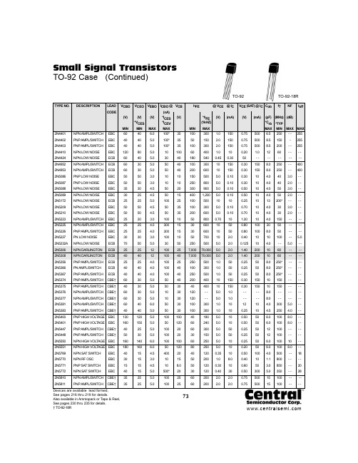
Small Signal Transistors TO-92 Case (Continued)73TYPE NO.DESCRIPTIONLEAD V CBOV CEO V EBO I CBO @V CBh FE@ V CE @ I C V CE (SA T) @ I C C obf TNFt offCODE(nA)(V)(V)(V)*I CES (V)*h FE (V)(mA) (V)(mA)(pF)(MHz)(dB)*V CES *I CEV (1kHZ)*C rb *TYPMIN MIN MAX MAX MIN MAX MAX MIN MAX MAX 2N4401NPN AMPL/SWITCH EBC 6040 6.0100*35100300 1.01500.75500 6.5250- -2552N4402PNP AMPL/SWITCH EBC 4040 5.0100*3550150 2.01500.755008.5150- 2552N4403PNP AMPL/SWITCH EBC 4040 5.0100*35100300 2.01500.755008.5200- -2552N4410NPN LOW NOISE EBC 12080 5.010******** 1.0100.20 1.01260- -- -2N4424NPN LOW NOISE ECB 6040 5.030401805400.450.3050- -- -- -- -- -2N4952NPN AMPL/SWITCH ECB 6030 5.05040100300101500.301508.0250- -4002N4953NPN AMPL/SWITCH ECB 6030 5.05040200600101500.301508.0250- -4002N5086PNP LOW NOISE EBC 5050 3.010******** 5.00.100.3010 4.040 3.0- -2N5087PNP LOW NOISE EBC 5050 3.010******** 5.00.100.3010 4.040 2.0- -2N5088NPN LOW NOISE EBC 3530 4.55020300900 5.00.100.5010 4.050 3.0- -2N5089NPN LOW NOISE EBC 3025 4.550154001,200 5.00.100.5010 4.050 2.0- -2N5172NPN LOW NOISE ECB 2525 5.01002510050010100.251013200*- -- -2N5209NPN LOW NOISE EBC 5050 4.55035100300 5.00.100.7010 4.030 3.0- -2N5210NPN LOW NOISE EBC 5050 4.55035200600 5.00.100.7010 4.030 2.0- -2N5223NPN AMPL/SWITCH EBC 2520 3.010*********.7010 1.2010 4.0150- -- -2N5225NPN AMPL/SWITCH EBC 2525 4.0300153060010500.801002050- -- -2N5226PNP AMPL/SWITCH EBC 2525 4.0300153060010500.801008.050- -- -2N5227PN LOW NOISE EBC 3030 3.0100105070010 2.00.401010100- - 5.02N5232A NPN LOW NOISE ECB 7050 5.03050250500 5.0 2.00.12510 4.0- - 5.0- -2N5306NPN DARLINGTON ECB 252512100257,00070,000 5.0 2.0 1.402001060- -- -2N5308NPN DARLINGTON ECB 404012100407,00070,000 5.0 2.0 1.402001060- -- -2N5356PNP AMPL/SWITCH ECB 2525 4.010********* 1.0500.25508.0250*- -- -2N5366PN AMPL/SWITCH ECB 4040 4.010********* 1.0500.25508.0250*- -- -2N5367PNP AMPL/SWITCH ECB 4040 4.010********* 1.0500.25508.0250*- -- -2N5374PNP AMPL/SWITCH CBE†6030 5.05040200400101500.3015010150- -- -2N5375PNP AMPL/SWITCH CBE†4030 5.0503040400101500.3015010150- -- -2N5376NPN AMPL/SWITCH CBE†6030 5.01030120- - 5.0 1.0- -- -8.0- -- -- -2N5377NPN AMPL/SWITCH CBE†6030 5.01030120- - 5.0 1.0- -- -8.0- -- -- -2N5381NPN AMPL/SWITCH CBE†6040 6.05030100300 1.0101210 4.0300 5.0- -2N5383PNP AMPL/SWITCHCBE†4040 5.05030100300 1.0100.2510 4.5250 4.0- -2N5400PNP HIGH VOL T AGE EBC 130120 5.010********* 5.0100.5050 6.01008.0- -2N5401PNP HIGH VOL T AGE EBC 160150 5.05012060240 5.0100.5050 6.01008.0- -2N5447PNP AMPL/SWITCH CBE†4025 5.010******** 5.0500.255012100- -- -2N5448PNP AMPL/SWITCHCBE†5030 5.010******** 5.0500.255012100- -- -2N5550NPN HIGH VOL T AGE EBC 160140 6.010********* 5.0100.2550 6.010010- -2N5551NPN HIGH VOL T AGE EBC 180160 6.05012080250 5.0100.2050 6.01008.0- -2N5769NPN SA T SWITCH EBC 4015 4.540020401200.35100.50100 4.0500- -182N5770NPN RF OSC EBC 3015 3.010******* 1.08.00.4010 1.1800- -- -2N5771PNP SA T SWITCH EBC 1515 4.5108.0501200.30100.6050 3.0850- -202N5772NPN SA T SWITCH EBC 4015 5.0500*20301200.40300.50300 5.0350- -282N5810NPN AMPL/SWITCH CBE†3525 5.010******** 2.0 2.00.7550015100- -- -2N5811PNP AMPL/SWITCHCBE†35255.010025602002.02.00.7550015100- -- -See pages 216 thru 219 for details.Also available in Ammopack or T ape & Reel,See pages 230 thru 235 for details.† TO-92-18RTO-92TO-92-18R元器件交易网。
常用三极管参数大全
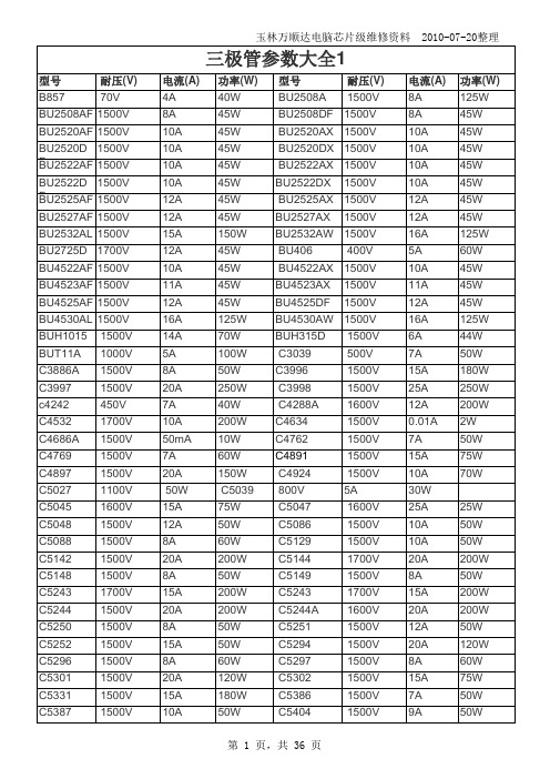
玉林万顺达电脑芯片级维修资料 2010-07-20整理玉林万顺达电脑芯片级维修资料 2010-07-20整理玉林万顺达电脑芯片级维修资料 2010-07-20整理玉林万顺达电脑芯片级维修资料 2010-07-20整理玉林万顺达电脑芯片级维修资料 2010-07-20整理玉林万顺达电脑芯片级维修资料 2010-07-20整理玉林万顺达电脑芯片级维修资料 2010-07-20整理玉林万顺达电脑芯片级维修资料 2010-07-20整理玉林万顺达电脑芯片级维修资料 2010-07-20整理玉林万顺达电脑芯片级维修资料 2010-07-20整理玉林万顺达电脑芯片级维修资料 2010-07-20整理玉林万顺达电脑芯片级维修资料 2010-07-20整理玉林万顺达电脑芯片级维修资料 2010-07-20整理玉林万顺达电脑芯片级维修资料 2010-07-20整理玉林万顺达电脑芯片级维修资料 2010-07-20整理玉林万顺达电脑芯片级维修资料 2010-07-20整理玉林万顺达电脑芯片级维修资料 2010-07-20整理玉林万顺达电脑芯片级维修资料 2010-07-20整理玉林万顺达电脑芯片级维修资料 2010-07-20整理玉林万顺达电脑芯片级维修资料 2010-07-20整理玉林万顺达电脑芯片级维修资料 2010-07-20整理玉林万顺达电脑芯片级维修资料 2010-07-20整理玉林万顺达电脑芯片级维修资料 2010-07-20整理玉林万顺达电脑芯片级维修资料 2010-07-20整理玉林万顺达电脑芯片级维修资料 2010-07-20整理玉林万顺达电脑芯片级维修资料 2010-07-20整理玉林万顺达电脑芯片级维修资料 2010-07-20整理玉林万顺达电脑芯片级维修资料 2010-07-20整理玉林万顺达电脑芯片级维修资料 2010-07-20整理玉林万顺达电脑芯片级维修资料 2010-07-20整理。
1N5280中文资料

rzjt and rzjk at Izk
mA A
IR 2) at VR
(1)The Zener impedance is derived from the 60Hz Ac voltage which results when an AC current having an RMS value equal to 10% of the Zener current (IZT) is suprimposed on IZT or IZK Zener impedance is measured at two points to insure a sharp knee on the breakdown curve and to eliminate unstable units. (2)Valid provided that leads at a distance of 8mm from case are kept at ambient temperature. (3) Measured under thermal equilibrium and DC test conditions.
1N5221…1N5249 SILICON PLANAR ZENER DIODES
Maximum Reverse Zener Voltage Range1) Type VZNOM 3) V 1N5221 1N5222 1N5223 1N5224 1N5225 1N5226 1N5227 1N5228 1N5229 1N5230 1N5231 1N5232 1N5233 1N5234 1N5235 1N5236 1N5237 1N5238 1N5239 1N5240 1N5241 1N5242 1N5243 1N5244 1N5245 1N5246 1N5247 1N5248 1N5249 2.4 2.5 2.6 2.8 3.0 3.3 3.6 3.9 4.3 4.7 5.1 5.6 6.0 6.2 6.8 7.5 8.2 8.7 9.1 10 11 12 13 14 15 16 17 18 19 9.5 9.0 8.5 7.8 7.4 7.0 6.6 20 <29 <28 <24 <23 <22 <19 <17 <11 <7 <7 <5 <6 <8 <8 <10 <17 <22 <30 <13 <15 <16 <17 <19 <21 <23 0.1 <600 <2 <1 <0.5 <30 IZT mA <1200 <1250 <1300 <1400 <1600 <1600 <1700 <1900 <2000 <1900 <1600 <1600 <1600 <1000 <750 <500 <500 3 0.25 5 2.0 2.0 3.0 3.5 4.0 5.0 6.0 6.5 6.5 7.0 8.0 8.4 9.1 9.9 10 11 12 13 14 14 Maximum zener impedance 1) Leakage Current
2N5657中文资料

2N5657SILICON NPN TRANSISTORs SGS-THOMSON PREFERRED SALESTYPE sNPN TRANSISTORDESCRIPTIONThe 2N5657is a silicon epitaxial-base NPN transistor in Jedec SOT-32plastic package.It is intended for use output amplifiers,low current,high voltage converters and AC line relays.INTERNAL SCHEMATIC DIAGRAMJune 1997ABSOLUTE MAXIMUM RATINGSSymbol ParameterValue Unit V CBO Collector-Base Voltage (I E =0)375V V CEO Collector-Emitter Voltage (I B =0)350V V EBO Emitter-Base Voltage (I C =0)6V I C Collector Current 0.5A I CM Collector Peak Current 1A I B Base Current0.25A P t ot Total Dissipation at T c ≤25oC 20WT stg Storage Temperature-65to 150o C T jMax.Operating Junction Temperature150oC 321SOT-321/5THERMAL DATAR t hj-ca se Thermal Resistance Junction-case Max 6.25o C/W ELECTRICAL CHARACTERISTICS(T case=25o C unless otherwise specified)Symbol Parameter Test Conditions Min.Typ.Max.UnitI CBO Collector Cut-offCurrent(I E=0)V CE=375V0.01mAI CEV Collector Cut-offCurrent(V BE=-1.5V)V CE=350VV CE=250V T c=100o C0.11mAmAI CEO Collector Cut-offCurrent(I B=0)V CE=250V0.1mAI EBO Emitter Cut-off Current(I C=0)V EB=6V0.01mAV(BR)CEO∗Collector-EmitterBreakdown VoltageI C=1mA350VV CEO(sus)∗Collector-EmitterSustaining VoltageI C=100mA L=50mH350VV CE(sat)∗Collector-EmitterSaturation Voltage I C=0.1A I B=10mAI C=0.25A I B=25mAI C=0.5A I B=0.1A12.510VVVV BE∗Base-Emitter Voltage I C=0.1A V CE=10V1Vh FE∗DC Current Gain I C=50mA V CE=10VI C=0.1A V CE=10VI C=0.25A V CE=10VI C=0.5A V CE=10V 2530155250h f e Small Signal CurrentGainI C=0.1A V CE=10V f=1KHz20f T Transition frequency I C=50mA V CE=10V f=10MHz10MHzC CBO Collector BaseCapacitanceV CB=10V f=100KHz25pF ∗ Pulsed:Pulse duration=300µs,duty cycle1.5%Safe Operating Area Derating Curve2N56572/5DC Current Gain(NPN type)Collector Emitter Saturation Voltage(NPN type)DC Current Gain(PNP type)Collector Emitter Saturation Voltage(PNP type)2N56573/5DIM.mm inch MIN.TYP.MAX.MIN.TYP.MAX.A 7.47.80.2910.307B 10.510.80.4130.445b 0.70.90.0280.035b10.490.750.0190.030C 2.4 2.70.0400.106c1 1.0 1.30.0390.050D 15.416.00.6060.629e 2.20.087e3 4.154.650.1630.183F 3.80.150G 3 3.20.1180.126H 2.540.100H22.150.084H20016114SOT-32(TO-126)MECHANICAL DATA2N56574/52N5657 Information furnished is believed to be accurate and reliable.However,SGS-THOMSON Microelectronics assumes no responsability for the consequences of use of such information nor for any infringementof patents or other rights of third parties which may results from its use.No license is granted by implication or otherwise under any patent or patent rights of SGS-THOMSON Microelectronics.Specifications mentionedin this publication are subject to change without notice.This publicationsupersedes and replaces all information previously supplied.SGS-THOMSON Microelectronics products are notauthorized for use as critical components in life support devices or systems without express written approval of SGS-THOMSON Microelectonics.©1997SGS-THOMSON Microelectronics-Printed in Italy-All Rights ReservedSGS-THOMSON Microelectronics GROUP OF COMPANIESAustralia-Brazil-Canada-China-France-Germany-Hong Kong-Italy-Japan-Korea-Malaysia-Malta-Morocco-The Netherlands-Singapore-Spain-Sweden-Switzerland-Taiwan-Thailand-United Kingdom-U.S.A...5/5。
2N2905A;中文规格书,Datasheet资料
2N2905A 2N2907ASMALL SIGNAL PNP TRANSISTORSDESCRIPTION The 2N2905A and 2N2907A are silicon Planar Epitaxial PNP transistors in Jedec TO-39 (for 2N2905A) and in Jedec TO-18 (for 2N2907A)metal case. They are designed for high speed saturated switching and general purpose applications.February 2003ABSOLUTE MAXIMUM RATINGS®1/7THERMAL DATAELECTRICAL CHARACTERISTICS (T case = 25 oC unless otherwise specified)** See test circuit2N2905A/2N2907ANormalized DC Current Gain.Collector Emitter Saturation Voltage.Collector Base and Emitter-base capacitances.Switching Characteristics.2N2905A/2N2907A2N2905A/2N2907A.Test Circuit for t on, t r, t d ArrayTest Circuit for t off, t o, t f.2N2905A/2N2907A2N2905A/2N2907AInformation furnished is believed to be accurate and reliable. However, STMicroelectronics assumes no responsibility for the consequences of use of such information nor for any infringement of patents or other rights of third parties which may result from its use. No license is granted by implication or otherwise under any patent or patent rights of STMicroelectronics. Specification mentioned in this publication are subject to change without notice. This publication supersedes and replaces all information previously supplied. STMicroelectronics products are not authorized for use as critical components in life support devices or systems without express written approval of STMicroelectronics.The ST logo is a trademark of STMicroelectronics © 2003 STMicroelectronics – Printed in Italy – All Rights ReservedSTMicroelectronics GROUP OF COMPANIESAustralia - Brazil - Canada - China - Finland - France - Germany - Hong Kong - India - Israel - Italy - Japan - Malaysia - Malta - Morocco - Singapore - Spain - Sweden - Switzerland - United Kingdom - United States.2N2905A/2N2907A分销商库存信息: STM2N2905A。
2N5089中文资料

Amplifier TransistorsNPN SiliconMAXIMUM RATINGSTHERMAL CHARACTERISTICSELECTRICAL CHARACTERISTICS (T = 25°C unless otherwise noted)OFF CHARACTERISTICS1.R θJA is measured with the device soldered into a typical printed circuit board.2.Pulse Test: Pulse Width ≤ 300 m s, Duty Cycle ≤ 2.0%.ON Semiconductor t© Semiconductor Components Industries, LLC, 20011Publication Order Number:2N50882N5089COLLECTOR21EMITTERELECTRICAL CHARACTERISTICS (T= 25°C unless otherwise noted) (Continued)SMALL–SIGNAL CHARACTERISTICS2.Pulse Test: Pulse Width ≤ 300 m s, Duty Cycle ≤ 2.0%.Figure 2. Effects of Frequencyf, FREQUENCY (Hz)7.01020305.0Figure 3. Effects of Collector CurrentI C , COLLECTOR CURRENT (mA)Figure 4. Noise Currentf, FREQUENCY (Hz)Figure 5. Wideband Noise FigureR S , SOURCE RESISTANCE (OHMS)3.0NOISE CHARACTERISTICS(V CE = 5.0 Vdc, T A = 25°C)NOISE VOLTAGEe n , N O I S E V O L T A G E (n V )e n , N O IS E V O L T A G E (n V )I n , N O I S E C U R R E N T (p A )N F , N O I S E F I G U R E (d B )7.01020305.03.0100.10.20.31.00.72.03.05.07.004.08.0121620100 Hz NOISE DATA3002001003.05.07.010********R S , SOURCE RESISTANCE (OHMS)V T , T O T A L N O I S E V O L T A G E (n V )N F , N O I S E F I G U R E (d B )4.08.01220Figure 6. Total Noise Voltage R S , SOURCE RESISTANCE (OHMS)Figure 7. Noise Figure0.5Figure 8. DC Current GainI C , COLLECTOR CURRENT (mA)0.41.02.03.04.00.3h , D C C U R R E N T G A I N (N O R M A L I Z E D )0.2F E 0.70.5Figure 9. “On” VoltagesI C , COLLECTOR CURRENT (mA)0.40.60.81.00.2Figure 10. Temperature CoefficientsI C , COLLECTOR CURRENT (mA)V , V O L T A G E (V O L T S )-ā0.8-ā1.2-ā1.6-ā2R V B E ,B A S E -E M I T T E R θT E M P ER A T U R E C O E F F I C I E N T (m V /C )°-ā0.4-ā2.0f T , C U R R E N T -G A I N Ċ B A N D W I D T H P R O D U C T (M H z )C , C A P A C I T A N C E (p F )8.00.81.02.03.04.06.05003002007050100Figure 11. Capacitance V R , REVERSE VOLTAGE (VOLTS)Figure 12. Current–Gain — Bandwidth ProductI C , COLLECTOR CURRENT (mA)PACKAGE DIMENSIONSCASE 29–11ISSUE ALTO–92 (TO–226)NOTES:1.DIMENSIONING AND TOLERANCING PER ANSI Y14.5M, 1982.2.CONTROLLING DIMENSION: INCH.3.CONTOUR OF PACKAGE BEYOND DIMENSION R IS UNCONTROLLED.4.LEAD DIMENSION IS UNCONTROLLED IN P AND BEYOND DIMENSION K MINIMUM.PLANEDIM MIN MAX MIN MAX MILLIMETERSINCHES A 0.1750.205 4.45 5.20B 0.1700.210 4.32 5.33C 0.1250.165 3.18 4.19D 0.0160.0210.4070.533G 0.0450.055 1.15 1.39H 0.0950.105 2.42 2.66J 0.0150.0200.390.50K 0.500---12.70---L 0.250--- 6.35---N 0.0800.105 2.04 2.66P ---0.100--- 2.54R 0.115--- 2.93---V0.135--- 3.43---EMITTER2.BASE3.COLLECTORON Semiconductor and are trademarks of Semiconductor Components Industries, LLC (SCILLC). SCILLC reserves the right to make changes without further notice to any products herein. SCILLC makes no warranty, representation or guarantee regarding the suitability of its products for any particular purpose, nor does SCILLC assume any liability arising out of the application or use of any product or circuit, and specifically disclaims any and all liability, including without limitation special, consequential or incidental damages. “Typical” parameters which may be provided in SCILLC data sheets and/or specifications can and do vary in different applications and actual performance may vary over time. All operating parameters, including “Typicals” must be validated for each customer application by customer’s technical experts. SCILLC does not convey any license under its patent rights nor the rights of others.SCILLC products are not designed, intended, or authorized for use as components in systems intended for surgical implant into the body, or other applications intended to support or sustain life, or for any other application in which the failure of the SCILLC product could create a situation where personal injury or death may occur. Should Buyer purchase or use SCILLC products for any such unintended or unauthorized application, Buyer shall indemnify and hold SCILLC and its officers, employees, subsidiaries, affiliates, and distributors harmless against all claims, costs, damages, and expenses, and reasonable attorney fees arising out of, directly or indirectly, any claim of personal injury or death associated with such unintended or unauthorized use, even if such claim alleges that SCILLC was negligent regarding the design or manufacture of the part. SCILLC is an Equal Opportunity/Affirmative Action Employer. PUBLICATION ORDERING INFORMATIONJAPAN: ON Semiconductor, Japan Customer Focus Center4–32–1 Nishi–Gotanda, Shinagawa–ku, Tokyo, Japan 141–0031Phone: 81–3–5740–2700Email: r14525@。
MMDT3946中文资料
N+P
N+P
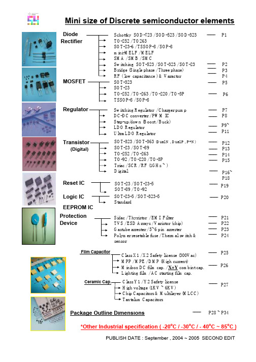
SOT-23 (P.28)
BC807 BC817 BC846 BC847 BC848 BC856 BC857 BC858 BCW65C MMBT1015 MMBT1815 MMBT2222A MMBT2369 MMBT2484 MMBT2907A MMBT3904 MMBT3906 MMBT4124 MMBT4125 MMBT4401 MMBT4403 MMBT5086 MMBT5087 MMBT5088 MMBT5089 MMBT5401 MMBT5550 MMBT5551 MMBT6427 MMBT6429 MMBT6517 MMBT6520 MMBT8050 MMBT8099 MMBT8550 MMBT8599 MMBT9018 MMBTA06 MMBTA13 MMBTA14
Ceramic Ckage Outline Dimensions
P28 ~ P34
o o
*Other Industrial specification ( -20 C / -30 C / - 40 C ~ 85 C )
PUBLISH DATE : September , 2004 ~ 2005 SECOND EDIT
BCE BCE BCE BCE BCE BCE BCE BCE DAUL DAUL DAUL DAUL DAUL DAUL DAUL DAUL
N+P
SOT-363 (P.29)
MMDT2412 MMDT3904 MMDT2222 MMDT2411 MMDT1036 MMDT1037 MMDT3906 MMDT2907 MMDT2227 MMDT3946
PNP NPN NPN NPN NPN PNP PNP PNP NPN PNP NPN NPN NPN NPN PNP NPN PNP NPN PNP NPN PNP PNP PNP NPN NPN PNP NPN NPN NPN NPN NPN PNP NPN NPN PNP PNP NPN NPN NPN NPN -50 50 80 50 30 -80 -50 -30 60 -50 60 75 40 60 -60 60 -40 30 -30 60 -40 -50 -50 35 30 -160 160 180 40 55 350 -350 25 80 -25 -80 20 80 30 30 -45 45 65 45 30 -65 -45 -30 32 -50 50 40 40 60 -60 40 -40 25 -30 40 -40 -50 -50 30 25 -150 140 160 40 45 350 -350 20 80 -20 -80 15 80 30 30 -800 800 100 100 100 -100 -100 -100 800 -150 150 600 500 50 -600 200 -200 200 -200 600 -600 -50 -50 50 50 -600 600 600 500 200 500 -500 700 500 -700 -500 50 500 300 300 225 225 225 225 225 225 225 225 225 225 225 225 225 225 225 225 225 225 225 225 225 225 225 225 225 225 225 225 225 225 225 225 225 225 225 225 225 225 225 225 100 100 110 110 110 115 110 110 250 120 120 100 40 250 100 100 120 120 50 100 100 150 250 300 400 60 60 80 20K 500 30 30 150 100 150 100 30 50 10K 20K 630 630 800 800 800 800 800 800 630 700 700 300 120 300 300 360 360 150 300 300 500 800 900 1200 240 250 250 200K 1250 200 200 500 300 400 300 400 -100 100 2 2 2 -2 -2 -2 100 -2 2 150 10 1 -150 10 -10 2 -2 150 -150 -0.1 -0.1 0.1 0.1 -10 10 10 100 0.1 30 -30 150 1 -150 -1 1 10 100 100 -1 1 5 5 5 -5 -5 -5 1 -6 6 10 1 5 -10 1 -1 1 -1 1 -2 -5 -5 5 5 -5 5 5 5 5 10 -10 1 5 -1 -5 6 1 5 5 -0.7 0.7 0.25 0.25 0.25 -0.3 -0.3 -0.3 0.3 -0.3 0.25 0.5 0.25 0.35 -0.4 0.2 0.25 0.3 -0.4 0.4 -0.4 -0.3 -0.3 0.5 0.5 -0.2 0.25 0.15 1.2 0.2 0.5 -0.5 0.5 0.4 -0.5 -0.4 0.5 0.25 1.5 1.5 -500 500 10 10 10 -10 -10 -10 100 -100 100 380 10 1 -150 10 -10 50 -50 150 -150 -10 -10 10 10 -10 50 10 50 10 30 -30 500 100 -500 -100 5 100 100 100 -50 50 0.5 0.5 0.5 -0.5 -0.5 -0.5 10 -10 10 10 1 0.1 -15 1 -1 5 -5 15 -15 -1 -1 1 1 -1 5 1 0.5 0.5 3 -3 50 5 -50 -5 0.5 10 0.1 0.1 100 40 40 150 150 150 150 500 100 125 125 200 300 250 300 200 250 200 40 40 50 50 100 100 100 100 100 300 300 300 150 150 150 170 80 80 300 500
2N5087中文资料

2N5087中⽂资料Amplifier TransistorPNP SiliconMAXIMUM RATINGSTHERMAL CHARACTERISTICSELECTRICAL CHARACTERISTICS (T = 25°C unless otherwise noted)OFF CHARACTERISTICS1.Pulse T est: Pulse Width ≤ 300 m s, Duty Cycle ≤2.0%.Preferred devices are ON Semiconductor recommended choices for future use and best overall value. ON Semiconductor tPublication Order Number:2N5087ON Semiconductor Preferred Device COLLECTOR21EMITTERELECTRICAL CHARACTERISTICS (T= 25°C unless otherwise noted) (Continued)1.Pulse T est: Pulse Width ≤ 300 m s, Duty Cycle ≤2.0%.TYPICAL NOISE CHARACTERISTICS(V CE = –5.0 Vdc, T A = 25°C)Figure 1. Noise Voltage f, FREQUENCY (Hz)5.07.0103.0Figure 2. Noise Currentf, FREQUENCY (Hz)1.01020100200500 1.0?k 2.0?k5.0?k10?ke n , N O I S E V O L T A G E (n V )102050100200500 1.0?k 2.0?k 5.0?k10?k2.0NOISE FIGURE CONTOURS(V CE = –5.0 Vdc, T A = 25°C)500?k 1002005001.0?k 10?k 5.0?k 20?k 50?k 100?k 200?k 2.0?k 1.0?M 500?k 1002005001.0?k 10?k 5.0?k 20?k 50?k 100?k 200?k 2.0?k 1.0?M Figure 3. Narrow Band, 100 Hz I C , COLLECTOR CURRENT (µA)Figure 4. Narrow Band, 1.0 kHzI C , COLLECTOR CURRENT (µA)10R S , S O UR CE R E S I S T A N C E (O H M S )R S , S O U R C E R E S I S T A N C E (O H M S )Figure 5. WidebandI C , COLLECTOR CURRENT (µA)10R S , S O U R C E R E S I S T A N C E (O H M S )Noise Figure is Defined as:NF +20log 10e n 2)4KTR S )I n 2R S 24KTR S1ń2= Noise Voltage of the Transistor referred to the input. (Figure 3)= Noise Current of the Transistor referred to the input. (Figure4)= Boltzman’s Constant (1.38 x 10⁻²³ j/°K)= T emperature of the Source Resistance (°K)= Source Resistance (Ohms)e n I n K T R S 203050701002003005007001.0?k10203050701002003005007001.0?k500?k 1002005001.0?k 10?k 5.0?k 20?k 50?k 100?k 200?k 2.0?k 1.0?M 203050701002003005007001.0?kh , D C C U R R E N T G A I NF E I C , COLLECTOR CURRENT (mA)1.4I C , COLLECTOR CURRENT (mA)V , V O L T A G E (V O L T S )Figure 9. “On” Voltages 0.40.60.81.00.2V C E , C O L L E C T O R -E M I T T E R V O L T A G E (V O L T S ) Figure 10. Temperature Coefficients1.21.00.80.60.40.20C , C A P A C I T A N C E (p F )Figure 11. Turn–On TimeI C , COLLECTOR CURRENT (mA)500Figure 12. Turn–Off TimeI C , COLLECTOR CURRENT (mA)Figure 13. Current–Gain — Bandwidth Product I C , COLLECTOR CURRENT (mA)Figure 14. Capacitance V R , REVERSE VOLTAGE (VOLTS)Figure 15. Input Impedance I C , COLLECTOR CURRENT (mA)Figure 16. Output AdmittanceI C , COLLECTOR CURRENT (mA)5000.510t , T I M E (n s )f ?, C U R R E N T -G A I N ? B A N D W I D T H P R O D U C T (M H z )T h i e , I N P U T I M P E D A N C E (k )5.07.010203050701003005070100200300 1.02.03.05.07.00.20.30.50.71.02.03.05.07.01020200-5.0-7.0-50-70Figure 17. Thermal Responset, TIME (ms)1.0r (t ) T R A N S I E N T T H E R M A L R E S I S T A N C E (N O R M A L I Z E D ) 0.010.020.030.050.070.10.20.30.50.750?kT J , JUNCTION TEMPERATURE (°C)104I C , C O L L E C T O R C U R R E N T (n A )Figure 19. Typical Collector Leakage Current400I C , C O L L E C T O R C U R R E N T (m A )DESIGN NOTE: USE OF THERMAL RESPONSE DATAA train of periodical power pulses can be represented by the model as shown in Figure 19. Using the model and the device thermal response the normalized effective transient thermal resistance of Figure 17 was calculated for various duty cycles. To find Z θJA(t), multiply the value obtained from Figure 17 by the steady state value R θJA .Example:The 2N5087 is dissipating 2.0 watts peak under the follow-ing conditions:t 1 = 1.0 ms, t 2 = 5.0 ms (D = 0.2)Using Figure 17 at a pulse width of 1.0 ms and D = 0.2, the reading of r(t) is 0.22.The peak rise in junction temperature is thereforeT = r(t) x P (pk) x R θJA = 0.22 x 2.0 x 200 = 88°C.For more information, see ON Semiconductor Application Note AN569/D, available from the Literature Distribution Center or on our website at/doc/08656144e518964bcf847c95.html .The safe operating area curves indicate I C –V CE limits of the transistor that must be observed for reliableoperation.Collector load lines for specific circuits must fall below the limits indicated by the applicable curve.The data of Figure 18 is based upon T J(pk) = 150°C; T C or T A is variable depending upon conditions. Pulse curves are valid for duty cycles to 10% provided T J(pk) ≤ 150°C. T J(pk)may be calculated from the data in Figure 17. At high case or ambient temperatures, thermal limitations will reduce the power than can be handled to values less than the limitations imposed by second breakdown.10-210-11001011021034.06.010204060100200PACKAGE DIMENSIONSCASE 29–11ISSUE ALTO–92 (TO–226)NOTES:1.DIMENSIONING AND TOLERANCING PER ANSI Y14.5M, 1982.2.CONTROLLING DIMENSION: INCH.3.CONTOUR OF PACKAGE BEYOND DIMENSION R IS UNCONTROLLED.4.LEAD DIMENSION IS UNCONTROLLED IN P AND BEYOND DIMENSION K MINIMUM.DIM MIN MAX MIN MAX MILLIMETERSINCHES A 0.1750.205 4.45 5.20B 0.1700.210 4.32 5.33C 0.1250.165 3.18 4.19D 0.0160.0210.4070.533G 0.0450.055 1.15 1.39H 0.0950.105 2.42 2.66J 0.0150.0200.390.50K 0.500---12.70---L 0.250--- 6.35---N 0.0800.105 2.04 2.66P ---0.100--- 2.54R 0.115--- 2.93---V0.135--- 3.43---EMITTER2.BASE3.COLLECTORON Semiconductor and are trademarks of Semiconductor Components Industries, LLC (SCILLC). SCILLC reserves the right to make changes without further notice to any products herein. SCILLC makes no warranty, representation or guarantee regarding the suitability of its products for any particular purpose, nor does SCILLC assume any liability arising out of the application or use of any product or circuit, and specifically disclaims any and all liability, including without limitation special, consequential or incidental damages. “Typical” parameters which may be provided in SCILLC data sheets and/or specifications can and do vary in different applications and actual performance may vary over time. All operating parameters, including “Typicals” must be validated for each customer application by customer’s technical experts. SCILLC does not convey any license under its patent rights nor the rights of others.SCILLC products are not designed, intended, or authorized for use as components in systems intended for surgical implant into the body, or other applications intended to support or sustain life, or for any other application in which the failure of the SCILLC product could create a situation where personal injury or death may occur. Should Buyer purchase or use SCILLC products for any such unintended or unauthorized application, Buyer shall indemnify and hold SCILLC and its officers, employees, subsidiaries, affiliates, and distributors harmless against all claims, costs, damages, and expenses, and reasonable attorney fees arising out of, directly or indirectly, any claim of personal injury or death associated with such unintended or unauthorized use, even if such claim alleges that SCILLC was negligent regarding the design or manufacture of the part. SCILLC is an Equal Opportunity/Affirmative Action Employer. PUBLICATION ORDERING INFORMATION JAPAN: ON Semiconductor, Japan Customer Focus Center4–32–1 Nishi–Gotanda, Shinagawa–ku, Tokyo, Japan 141–0031Phone: 81–3–5740–2700Email: r14525@/doc/08656144e518964bcf847c95.html。
- 1、下载文档前请自行甄别文档内容的完整性,平台不提供额外的编辑、内容补充、找答案等附加服务。
- 2、"仅部分预览"的文档,不可在线预览部分如存在完整性等问题,可反馈申请退款(可完整预览的文档不适用该条件!)。
- 3、如文档侵犯您的权益,请联系客服反馈,我们会尽快为您处理(人工客服工作时间:9:00-18:30)。
Amplifier TransistorPNP SiliconMAXIMUM RATINGSTHERMAL CHARACTERISTICSELECTRICAL CHARACTERISTICS (T = 25°C unless otherwise noted)OFF CHARACTERISTICS1.Pulse T est: Pulse Width ≤ 300 m s, Duty Cycle ≤2.0%.Preferred devices are ON Semiconductor recommended choices for future use and best overall value.ON Semiconductor t1Publication Order Number:2N5087ON Semiconductor Preferred DeviceCOLLECTOR21EMITTERELECTRICAL CHARACTERISTICS (T= 25°C unless otherwise noted) (Continued)1.Pulse T est: Pulse Width ≤ 300 m s, Duty Cycle ≤2.0%.TYPICAL NOISE CHARACTERISTICS(V CE = –5.0 Vdc, T A = 25°C)Figure 1. Noise Voltage f, FREQUENCY (Hz)5.07.0103.0Figure 2. Noise Currentf, FREQUENCY (Hz)1.0102050100200500 1.0Ăk 2.0Ăk5.0Ăk10Ăke n , N O I S E V O L T A G E (n V )102050100200500 1.0Ăk 2.0Ăk 5.0Ăk10Ăk2.0NOISE FIGURE CONTOURS(V CE = –5.0 Vdc, T A = 25°C)500Ăk 1002005001.0Ăk 10Ăk 5.0Ăk 20Ăk 50Ăk 100Ăk 200Ăk 2.0Ăk 1.0ĂM 500Ăk 1002005001.0Ăk 10Ăk 5.0Ăk 20Ăk 50Ăk 100Ăk 200Ăk 2.0Ăk 1.0ĂM Figure 3. Narrow Band, 100 Hz I C , COLLECTOR CURRENT (µA)Figure 4. Narrow Band, 1.0 kHzI C , COLLECTOR CURRENT (µA)10R S , S O UR CE R E S I S T A N C E (O H M S )R S , S O U R C E R E S I S T A N C E (O H M S )Figure 5. WidebandI C , COLLECTOR CURRENT (µA)10R S , S O U R C E R E S I S T A N C E (O H M S )Noise Figure is Defined as:NF +20log 10ƪe n 2)4KTR S )I n 2R S 24KTR Sƫ1ń2= Noise Voltage of the Transistor referred to the input. (Figure 3)= Noise Current of the Transistor referred to the input. (Figure 4)= Boltzman’s Constant (1.38 x 10⁻²³ j/°K)= T emperature of the Source Resistance (°K)= Source Resistance (Ohms)e n I n K T R S 203050701002003005007001.0Ăk10203050701002003005007001.0Ăk500Ăk 1002005001.0Ăk 10Ăk 5.0Ăk 20Ăk 50Ăk 100Ăk 200Ăk 2.0Ăk 1.0ĂM 203050701002003005007001.0Ăkh , D C C U R R E N T G A I NF E I C , COLLECTOR CURRENT (mA)1.4I C , COLLECTOR CURRENT (mA)V , V O L T A G E (V O L T S )Figure 9. “On” Voltages 0.40.60.81.00.2V C E , C O L L E C T O R -E M I T T E R V O L T A G E (V O L T S )Figure 10. Temperature Coefficients1.21.00.80.60.40.20C , C A P A C I T A N C E (p F )Figure 11. Turn–On TimeI C , COLLECTOR CURRENT (mA)500Figure 12. Turn–Off TimeI C , COLLECTOR CURRENT (mA)Figure 13. Current–Gain — Bandwidth Product I C , COLLECTOR CURRENT (mA)Figure 14. CapacitanceV R , REVERSE VOLTAGE (VOLTS)Figure 15. Input Impedance I C , COLLECTOR CURRENT (mA)Figure 16. Output AdmittanceI C , COLLECTOR CURRENT (mA)5000.510t , T I M E (n s )f ă, C U R R E N T -G A I N Ċ B A N D W I D T H P R O D U C T (M H z )T h i e , I N P U T I M P E D A N C E (k )Ω 5.07.010203050701003005070100200300 1.02.03.05.07.00.20.30.50.71.02.03.05.07.01020200-5.0-7.0-50-70Figure 17. Thermal Responset, TIME (ms)1.0r (t ) T R A N S I E N T T H E R M A L R E S I S T A N C E (N O R M A L I Z E D )0.010.020.030.050.070.10.20.30.50.750ĂkT J , JUNCTION TEMPERATURE (°C)104I C , C O L L E C T O R C U R R E N T (n A )Figure 19. Typical Collector Leakage Current400I C , C O L L E C T O R C U R R E N T (m A )DESIGN NOTE: USE OF THERMAL RESPONSE DATAA train of periodical power pulses can be represented by the model as shown in Figure 19. Using the model and the device thermal response the normalized effective transient thermal resistance of Figure 17 was calculated for various duty cycles.To find Z θJA(t), multiply the value obtained from Figure 17 by the steady state value R θJA .Example:The 2N5087 is dissipating 2.0 watts peak under the follow-ing conditions:t 1 = 1.0 ms, t 2 = 5.0 ms (D = 0.2)Using Figure 17 at a pulse width of 1.0 ms and D = 0.2, the reading of r(t) is 0.22.The peak rise in junction temperature is therefore∆T = r(t) x P (pk) x R θJA = 0.22 x 2.0 x 200 = 88°C.For more information, see ON Semiconductor Application Note AN569/D, available from the Literature Distribution Center or on our website at .The safe operating area curves indicate I C –V CE limits of the transistor that must be observed for reliable operation.Collector load lines for specific circuits must fall below the limits indicated by the applicable curve.The data of Figure 18 is based upon T J(pk) = 150°C; T C or T A is variable depending upon conditions. Pulse curves are valid for duty cycles to 10% provided T J(pk) ≤ 150°C. T J(pk)may be calculated from the data in Figure 17. At high case or ambient temperatures, thermal limitations will reduce the power than can be handled to values less than the limitations imposed by second breakdown.10-210-11001011021034.06.010204060100200PACKAGE DIMENSIONSCASE 29–11ISSUE ALTO–92 (TO–226)NOTES:1.DIMENSIONING AND TOLERANCING PER ANSI Y14.5M, 1982.2.CONTROLLING DIMENSION: INCH.3.CONTOUR OF PACKAGE BEYOND DIMENSION R IS UNCONTROLLED.4.LEAD DIMENSION IS UNCONTROLLED IN P AND BEYOND DIMENSION K MINIMUM.DIM MIN MAX MIN MAX MILLIMETERSINCHES A 0.1750.205 4.45 5.20B 0.1700.210 4.32 5.33C 0.1250.165 3.18 4.19D 0.0160.0210.4070.533G 0.0450.055 1.15 1.39H 0.0950.105 2.42 2.66J 0.0150.0200.390.50K 0.500---12.70---L 0.250--- 6.35---N 0.0800.105 2.04 2.66P ---0.100--- 2.54R 0.115--- 2.93---V0.135--- 3.43---EMITTER2.BASE3.COLLECTORON Semiconductor and are trademarks of Semiconductor Components Industries, LLC (SCILLC). SCILLC reserves the right to make changes without further notice to any products herein. SCILLC makes no warranty, representation or guarantee regarding the suitability of its products for any particular purpose, nor does SCILLC assume any liability arising out of the application or use of any product or circuit, and specifically disclaims any and all liability, including without limitation special, consequential or incidental damages. “Typical” parameters which may be provided in SCILLC data sheets and/or specifications can and do vary in different applications and actual performance may vary over time. All operating parameters, including “Typicals” must be validated for each customer application by customer’s technical experts. SCILLC does not convey any license under its patent rights nor the rights of others.SCILLC products are not designed, intended, or authorized for use as components in systems intended for surgical implant into the body, or other applications intended to support or sustain life, or for any other application in which the failure of the SCILLC product could create a situation where personal injury or death may occur. Should Buyer purchase or use SCILLC products for any such unintended or unauthorized application, Buyer shall indemnify and hold SCILLC and its officers, employees, subsidiaries, affiliates, and distributors harmless against all claims, costs, damages, and expenses, and reasonable attorney fees arising out of, directly or indirectly, any claim of personal injury or death associated with such unintended or unauthorized use, even if such claim alleges that SCILLC was negligent regarding the design or manufacture of the part. SCILLC is an Equal Opportunity/Affirmative Action Employer. PUBLICATION ORDERING INFORMATIONJAPAN: ON Semiconductor, Japan Customer Focus Center4–32–1 Nishi–Gotanda, Shinagawa–ku, Tokyo, Japan 141–0031Phone: 81–3–5740–2700Email: r14525@。