SF_2N5601中文资料
2N5551中文资料(fairchild)中文数据手册「EasyDatasheet - 矽搜」
50 VCB = 100V
10
10
10
1β
100 Co
o
125 C
0.1
o
-40 Co
25 Co
75 C
- CCEO(SALT)LECTOR-EMITTER VOLTAGE [V]
0.01
V
1
10
100
IC- COLLECTOR CURRENT [mA]
Figure 2. Collector-Emitter Saturation Voltage vs.
芯片中文手册,看全文,戳
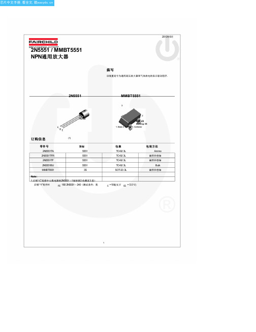
2N5551 / MMBT5551 NPN通用放大器
2013年6月
描写
该装置是专为通用高压放大器和气体放电的显示驱动程序.
2N5551
TO-92
MMBT5551
3
2
1 SOT-23
Marking: 3S 1. Base 2. Emitter 3. Collector
MMBT5551
350 2.8
357
Units
mW mW/°C °C/W °C/W
2
芯片中文手册,看全文,戳
电气特性
(4)
价值观是在T 符
A = 25°C除非另有说明. 参数
断特性
V(BR)CEO 集电极 - 发射极击穿电压 V(BR)CBO 集电极基击穿电压 V (BR)EBO 发射极基极击穿电压
Value
160 180
6 600 -55到+150
2N5551 / MMBT5551 - NPN通用放大
器
Units
V V V mA °C
热特性
价值观是在T
AD5621资料
REVISION HISTORY Revision PrC: Preliminary Version
Preliminary Technical Data
Input Shift Register .................................................................... 13 SYNC Interrupt .......................................................................... 14 Power-On Reset.......................................................................... 14 Power-Down Modes .................................................................. 14 Microprocessor Interfacing....................................................... 14 Applications..................................................................................... 16 Choosing a Reference as Power Supply for AD5601/AD5611/AD5621 ....................................................... 16 Bipolar Operation Using the AD5601/ AD5611/AD5621 .... 16 Using AD5601/AD5611/AD5621 with an Opto-Isolated Interface ....................................................................................... 17 Power Supply Bypassing and Grounding................................ 17 Outline Dimensions ....................................................................... 18 Ordering Guide .......................................................................... 18
2N5609中文资料
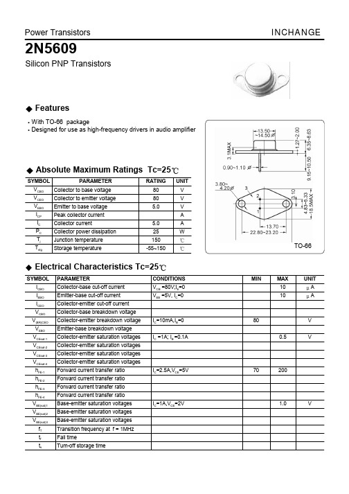
TO-66
Electrical Characteristics Tc=25
SYMBOL ICBO IEBO ICEO VCBO V(BR)CEO VEBO VCEsat-1 VCEsat-2 VCEsat-3 VCEsat-4 hFE-1 hFE-2 hFE-3 hFE-4 VBE(sat)1 VBE(sat)2 VBE(sat)3 fT tf ts PARAMETER Collector-base cut-off current Emitter-base cut-off current Collector-emitter cut-off current Collector-base breakdown voltage Collector-emitter breakdown voltage Emitter-base breakdown voltage Collector-emitter saturation voltages Collector-emitter saturation voltages Collector-emitter saturation voltages Collector-emitter saturation voltages Forward current transfer ratio Forward current transfer ratio Forward current transfer ratio Forward current transfer ratio Base-emitter saturation voltages Base-emitter saturation voltages Base-emitter saturation voltages Transition frequency at f = 1MHz Fall time Tum-off storage time IC=1A,VCE=2V 1.0 V IC=2.5A,VCE=5V 70 200 IC =1A; IB =0.1A 0.5 V IC=10mA,IB=0 80 V CONDITIONS VCB =80V;IE=0 VEB =5V, IC=0 MIN MAX 10 10 UNIT A A
TLC5602中文资料
IMPORTANT NOTICETexas Instruments (TI) reserves the right to make changes to its products or to discontinue any semiconductor product or service without notice, and advises its customers to obtain the latest version of relevant information to verify, before placing orders, that the information being relied on is current.TI warrants performance of its semiconductor products and related software to the specifications applicable at the time of sale in accordance with TI’s standard warranty. Testing and other quality control techniques are utilized to the extent TI deems necessary to support this warranty. Specific testing of all parameters of each device is not necessarily performed, except those mandated by government requirements.Certain applications using semiconductor products may involve potential risks of death, personal injury, or severe property or environmental damage (“Critical Applications”).TI SEMICONDUCTOR PRODUCTS ARE NOT DESIGNED, INTENDED, AUTHORIZED, OR WARRANTED TO BE SUITABLE FOR USE IN LIFE-SUPPORT APPLICATIONS, DEVICES OR SYSTEMS OR OTHER CRITICAL APPLICATIONS.Inclusion of TI products in such applications is understood to be fully at the risk of the customer. Use of TI products in such applications requires the written approval of an appropriate TI officer. Questions concerning potential risk applications should be directed to TI through a local SC sales office.In order to minimize risks associated with the customer’s applications, adequate design and operating safeguards should be provided by the customer to minimize inherent or procedural hazards.TI assumes no liability for applications assistance, customer product design, software performance, or infringement of patents or services described herein. Nor does TI warrant or represent that any license, either express or implied, is granted under any patent right, copyright, mask work right, or other intellectual property right of TI covering or relating to any combination, machine, or process in which such semiconductor products or services might be or are used.Copyright © 1995, Texas Instruments Incorporated。
SF5501中文资料

Phone: +86 10 6301 4184 Fax: +86 10 6301 9167 Email: sales@ Web: © April 2004 by Vanlong Technology Co., Ltd.SF5501• Ideal Front-End Filter for 401.65MHz Receivers • Low-Loss, Coupled-Resonator Quartz Design • Simple External Impedance Matching •Ultra Miniature Ceramic QCC8C PackageAbsolute Maximum Rating (Ta=25°C)Parameter Rating UnitInput Power Level P in 10 dBm DC Voltage V DC 12 V Operating Temperature RangeT A-10 ~ +60 °C Storage Temperature Range T stg -40 ~ +85°CElectronic CharacteristicsParameter SymMinimum Typical Maximum UnitNominal Frequency (25°C)(Center frequency between 3dB points) f C NS 401.65 NS MHz Insertion Loss IL - 3.0 5.0 dB 3dB Bandwidth BW 3- 550 - KHz Rejection at fc - 21.4 MHz (Image) at fc - 10.7 MHz (LO)Ultimate- - - 40 15 - 50 25 60 - - - dB dB dB Temperature StabilityOperating Temperature RangeTurnover Temperature Turnover FrequencyFrequency Temperature Coefficient T C T O f O FTC-10 25 - -- - f C 0.032 +60 55 - -°C °C KHz ppm/°CFrequency AgingAbsolute Value during the First Year|f A | - - 10 ppm/yr DC Insulation Resistance Between any Two Pins -1.0--M ΩNS = Not SpecifiedNotes:1. The frequency f C is defined as the midpoint between the 3dBfrequencies.2.Unless noted otherwise, all measurements are made with the filter installed in the specified test fixture that is connected to a 50Ω test system with VSWR ≤ 1.2:1. The test fixture L and C are adjusted for minimum insertion loss at the filter center frequency, f C . Note that insertion loss, bandwidth, and passband shape are dependent on the impedance matching component values and quality. 3. Unless noted otherwise, specifications apply over the entire specified operating temperature range.4.Frequency aging is the change in f C with time and is specified at +65°C or less. Aging may exceed the specification for prolonged temperatures above +65°C. Typically, aging is greatest the first year after manufacture, decreasing in subsequent years.5. Turnover temperature, T 0, is the temperature of maximum (orturnover) frequency, f 0. The nominal frequency at any casetemperature, T C , may be calculated from: f = f 0 [1 - FTC (T 0 - T C )2]. 6.The specifications of this device are based on the test circuit shown above and subject to change or obsolescence without notice.7. All equipment designs utilizing this product must be approved by the appropriate government agency prior to manufacture or sale. 8.Our liability is only assumed for the Surface Acoustic Wave (SAW) component(s) per se, not for applications, processes and circuits implemented within components or assemblies.9.For questions on technology, prices and delivery please contact our sales offices or e-mail sales@.SF5501Phone: +86 10 6301 4184 Fax: +86 10 6301 9167 Email: sales@ Web: © April 2004 by Vanlong Technology Co., Ltd.SF5501Package Dimensions (QCC8C)MarkingTest CircuitTypical Frequency ResponseElectrical ConnectionsTerminalsConnection 1 Input Ground2 Input5 Output Ground6 Output3,7 To be Grounded 4,8Case GroundPackage Dimensions DimensionsNom (mm) DimensionsNom (mm)A 2.08 E 1.20 B 0.60 F 1.35 C 1.27 G 5.00 D2.54H5.00C = 8.2 pFLs1 = Ls2 = 5 tunes of 0.5mm insulated copper, 2.0 ID.1. F5501 - Part Code2.Frequency (MHz) in 6 digits 3. Date Code:Y : Last digit of year WW : Week No.。
2N5551中文资料_数据手册_参数

Packing Method Ammo
Tape and Reel Tape and Reel
Bulk Tape and Reel
© 2009 Fairchild Semiconductor Corporation
Top Mark 5551 5551 5551 5551 3S
Package TO-92 3L TO-92 3L TO-92 3L TO-92 3L SOT-23 3L
Note: 1. Suffix “-C” means Center Collector in 2N5551 (1. Emitter 2. Collector 3. Base)
Symbol
Parameter
Value
Units
VCEO VCBO VEBO
IC TJ, Tstg(2)
Collector-Emitter Voltage Collector-Base Voltage Emitter-Base Voltage Collector current - Continuous Junction and Storage Temperature
2N5551 / MMBT5551 Rev. 1.1.0
1
2N5551 / MMBT5551 — NPN General-Purpose Amplifier
Absolute Maximum Ratings(2)
Stresses exceeding the absolute maximum ratings may damage the device. The device may not function or be operable above the recommended operating conditions and stressing the parts to these levels is not recommended. In addition, extended exposure to stresses above the recommended operating conditions may affect device reliability. The absolute maximum ratings are stress ratings only. Values are at TA = 25°C unless otherwise noted.
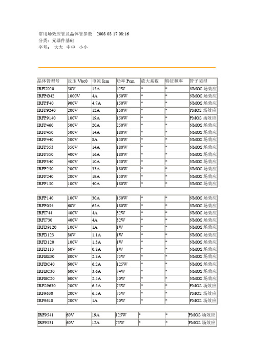
常用场效应管与三极管参数
150W
*
*
NPN
BU2522
1500V
11A
150W
*
*
NPN
BU2520
800V
10A
150W
*
*
NPN
BU2508
700V
8A
125W
*
*
NPN
BU2506
1500V
7A
50W
*
*
NPN
BU932R
500V
15A
150W
*
*
NPN
BU806
400V
8A
60W
*
*
NPN
BU406
400V
7A
50V
0.1A
0.4W
*
150MHZ
NPN
9013
50V
0.5A
0.6W
*
*
NPN
9012
50V
0.5A
0.6W
*
*
PNP
9011
50V
0.03A
0.4W
*
150MHZ
NPN
TIP147
100V
10A
125W
*
*
PNP
TIP142
100V
10A
125W
*
*
NPN
TIP127
100V
8A
65W
*
*
PNP
650V
15A
175W
*
*
NPN
2N5685
60V
50A
300W
*
*
NPN
2N6277
菲尼克斯电气开关电源中文样本
INTERFACE创新电源——系统的可靠保证菲尼克斯电气中国公司地址:南京市江宁开发区菲尼克斯路36号南京江宁236信箱电话:(025)52121888传真:(025)52121555/800 8289722邮编:211100h t t p: //e-mail: phoenix@ CN 11/12 INTERFACE 创新电源TNR 5768710/10.2011-01 Printed In China© PHOENIX CONTACT2011突破性技术——电源解决方案创新促进发展。
菲尼克斯电气的电源产品无疑印证了这一宗旨。
在对理想的电源探索中,我们洞悉市场,与客户密切合作,坚持与执着,不断创造出卓越的新产品技术。
我们的目标是最大程度提高您的设备和系统的可用性。
QUINT电源提供最优产品功能,三个新产品系列在各自领域里树立了新的标杆。
新产品采用ACB技术的冗余模块ACB(自动电流平衡)技术可使您的冗余电源系统的使用寿命翻倍。
该技术确保一定范围内所有的电源平衡输出。
QUINT ORING冗余模块的ACB技术还可检测临界工作状态,并为您提供提前预警。
新产品采用IQ技术的不间断电源具有持续电池监控和智能管理功能的IQ技术可随时为您提供电池的充电状态、剩余工作时间和使用寿命等相关信息。
智能通信功能将预警您危险工况的出现。
这可减少维护工作量,提升系统可用性。
新产品采用SFB技术的DC/DC变换器SFB(选择性触发)技术可在一旦输出回路出现短路时,可靠地切断故障回路。
在短路情况下,将能提供6倍额定输出电流,维持12ms时间。
因此,SFB技术能够可靠地触发标准断路器。
您可快速地进行故障定位,并确保系统的重要设备继续工作。
——采用SFB技术为系统有效性提供最高保证新一代紧凑型QUINT电源,将最大程度地保证系统的有效性。
该电源采用SFB技术(选择性触发技术),能在12ms内输出6倍的额定电流,可靠快速地触发标准断路器脱扣。