1.76微变lw13
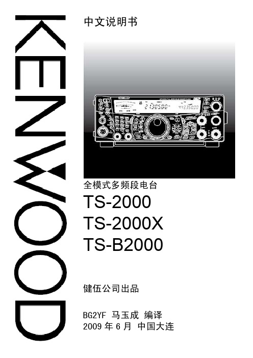
健伍TS-2000中文说明书
· 室外天线与电力线之间的距离最低应该保持天线及 其相关支撑结构的一倍半。这个距离才能保证一旦支 撑结构出现问题时不会影响到电力线路。
TS-2000:HF/ VHF/ UHF 全模式多频段电台 TS-2000X:HF/ VHF/ UHF/ 1.2 GHz 全模式多频段电台 TS-B2000:HF/ VHF/ UHF 全模式多频段电台
关于 TS-B2000 如何操作和控制电台,请参阅联机帮助。 安装和连接请参照第 2、3 和第 13 页。
· 电台的安放位置要通风良好。不要在电台上放置书籍 或其他设备,以免阻碍空气流动。电台后部与墙壁之 间最低保持 10 厘米的间隔。
· 不要在潮湿或靠近水的位置使用电台。例如,应避免 在浴缸、水槽、游泳池附近或在潮湿的地下室使用。
· 出现不正常的气味或烟雾往往是设备故障的表现。立 即关闭电源并拔下电源线,然后联系健伍服务站或您 的经销商。
数量
TS-2000 TS-2000X
TS-B2000
1
1
1
1
1
1
1
1
1
1
1
1
1
1
1
1
4
4
1
1
1
1
-
1
1
1
1
1
1
1
文档中的描述约定
为避免不必要的重复,以下的文档中将使用下表所列的
简化方式。
描述
操作方法
按[KEY]
按一下 KEY 键然后放开。
按住 KEY1 键不放,再按 KEY2 键。
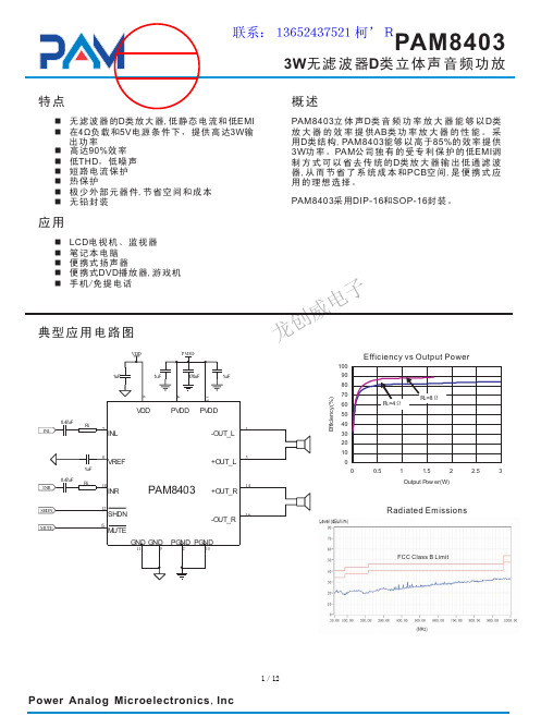
PAM8403中文规格书
n LCD
、
n
n
n
DVD
,
n
/
VDD
PVDD
1uF
1uF
470uF
1uF
13 4 6
0.47uF
Ri
INL
7
INL
VDD
PVDD PVDD
1
-OUT_L
8
VREF
1uF
0.47uF Ri INR
10
INR
3
+OUT_L
PAM8403
14
+OUT_R
SHDN MUTE
12
SHDN
5
MUTE
16
-OUT_R
,
1.0μF,
VDD
.
,
20μF(
)
.
(Ci)
,
.
.
, 100Hz 150Hz
(Ri)
fC= 1 2πRiCi
,
Ci
.
,
,
.,
.
(Ci)
,
,
(1/2 V ) DD . .
(C ) BYP
(CB ) YP .
.
, THD+N .
, CBYP
. PAM8403 PSRR
0.47μF 1.0μF
(C ) BYP
THD
.
/
.
/
V . DD .
.
VREF VREF
:PAM8403 ,
VREF .
,
. , 1/2
:
/
,
2
: VTH
1.3V@V = DD 5V,
/
, R1
LCTR-M偏芯测定换算表

LCTR-M偏芯测定换算表
LCTR-M偏芯测定换算表是一种用于测量电缆偏芯的工具,它可以帮助电缆制造商更准确地测量电缆偏芯的尺寸。
LCTR-M偏芯测定换算表可以测量电缆偏芯的长度、宽度和厚度,并将其转换为标准尺寸。
LCTR-M偏芯测定换算表的使用非常简单,只需将电缆偏芯放入换算表中,然后根据换算表上的标准尺寸,将其转换为标准尺寸。
这样,电缆制造商就可以更准确地测量电缆偏芯的尺寸,从而确保电缆的质量。
此外,LCTR-M偏芯测定换算表还可以用于测量电缆偏芯的其他参数,如电缆偏芯的外径、内径、折弯半径等。
这些参数对于确保电缆的质量至关重要,因此,使用LCTR-M偏芯测定换算表可以帮助电缆制造商更准确地测量电缆偏芯的参数,从而确保电缆的质量。
总之,LCTR-M偏芯测定换算表是一种非常有用的工具,可以帮助电缆制造商更准确地测量电缆偏芯的尺寸和参数,从而确保电缆的质量。
三垦vm06变频器使用说明书
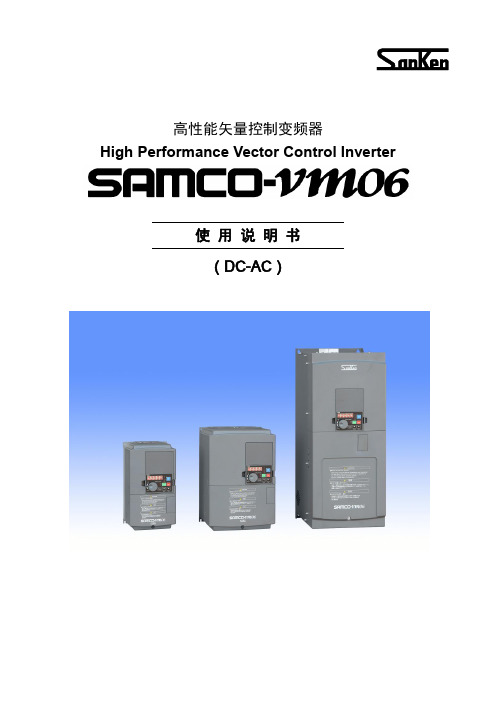
使用说明书 (DC-AC)
此次承蒙惠购
三垦高性能矢量控制变频器,深表谢意。
本变频器是为变速驱动感应电机的装置。由于内置了微处理器,故具备各种功能,操作也十分简便。为了
充分利用本机的功能,务必在使用之前,仔细阅读本使用说明书,以便于今后长期正确地使用。
4 配线 .................................................................................17
4-1 关于布线 ....................................................................................17 4-2 端子接线图 ..................................................................................18 4-3 主电路端子构成 ..............................................................................20
4
5-2-1 操作面板状态转换图...................................................................34
章
5-2-2 各种状态下的 LCD 显示.................................................................39
2 产品的确认和注意事项 .................................................................10
BCW66H 45V NPN 小信号转换器 SOT23 数据手册说明书
45V NPN SMALL SIGNAL TRANSISTOR IN SOT23Features∙ BV CEO > 45V ∙ I C = 800mA High Continuous Collector Current ∙ Low Saturation Voltage V CE(sat) < 300mV @ 100mA ∙ Complementary PNP Type: BCW68H∙ Totally Lead-Free & Fully RoHS compliant (Notes 1 & 2) ∙ Halogen and Antimony Free. “Green” Device (Note 3) ∙ Qualified to AEC-Q101 Standards for High Reliability ∙ PPAP capable (Note 4)Mechanical Data∙ Case: SOT23 ∙ Case Material: molded plastic, “Green” molding compound ∙ UL Flammability Classification Rating 94V-0 ∙ Moisture Sensitivity: Level 1 per J-STD-020∙ Terminals: Finish – Matte Tin Plated Leads, Solderable per MIL-STD-202, Method 208 ∙Weight 0.008 grams (approximate)Ordering Information (Notes 4 & 5)Part Number Compliance Marking Reel size (inches) Tape width (mm) Quantity per reel BCW66HTA AEC-Q101 EH 7 8 3,000 BCW66HQTA Automotive EH 7 8 3,000Notes: 1. No purposely added lead. Fully EU Directive 2002/95/EC (RoHS) & 2011/65/EU (RoHS 2) compliant.2. See /quality/lead_free.html for more information about Diodes Incorporated’s definitions of Halogen- and Antimony-free, "Green" and Lead-free.3. Halogen- and Antimony-free "Green” products are defined as those which contain <900ppm bromine, <900ppm chlorine (<1500ppm total Br + Cl) and <1000ppm antimony compounds.4. Automotive products are AEC-Q101 qualified and are PPAP capable. Automotive, AEC-Q101 and standard products are electrically and thermally the same, except where specified. For more information, please refer to /quality/product_compliance_definitions/.5. For packaging details, go to our website at /products/packages.html.Marking InformationEH = Product Type Marking CodeEHTop View Pin-OutCEBTop ViewDevice SymbolSOT23Maximum Ratings (@T A = +25°C, unless otherwise specified.)Characteristic Symbol Value UnitCollector-Base Voltage V CBO 75 V Collector-Emitter Voltage V CEO 45 V Emitter-Base Voltage V EBO 7 V Continuous Collector Current I C 800 mA Peak Pulse Current I CM 1000 mA Base Current I B 100 mAThermal Characteristics (@T A = +25°C, unless otherwise specified.)Characteristic Symbol Value UnitPower Dissipation (Note 6) P D310mW (Note 7) 350Thermal Resistance, Junction to Ambient (Note 6)R θJA403 ︒C/W (Note 7) 357Thermal Resistance, Junction to Leads (Note 8) R θJL 350 ︒C/W Operating and Storage Temperature Range T J,T STG-55 to +150 ︒C Notes:6. For a device mounted on minimum recommended pad layout 1oz weight copper that is on a single-sided FR4 PCB; device is measured under still airconditions whilst operating in a steady-state.7. Same as Note 6, except the device is mounted on 15mm X 15mm 1oz copper.8. Thermal resistance from junction to solder-point (at the end of the leads).Transient Thermal ImpedancePulse Width (s)Pulse Power DissipationPulse Width (s)MElectrical Characteristics (@T A = +25°C, unless otherwise specified.)Characteristic Symbol Min Typ Max Unit Test ConditionOFF CHARACTERISTICSCollector-Base Breakdown Voltage BV CES 75 — — V I C = 10µA Collector-Emitter Breakdown Voltage (base open) (Note 9)BV CEO45 — — V I CEO = 10mAEmitter-Base Breakdown Voltage BV EBO 7 — — V I EBO = 10µACollector-Emitter Cut-Off Current I CES— — <1 — 20 20 nAµA V CES = 45V V CES = 45V, T A = +150°CEmitter-Base Cut-Off Current I EBO — <1 20 nA V EBO = 5.6V ON CHARACTERISTICS (Note 9)Static Forward Current Transfer Ratio h FE80 180 250 100 — — 350 — ——630 — — I C = 100µA, V CE = 10V I C = 10mA, V CE = 1V I C = 100mA, V CE = 1V I C = 500mA, V CE = 2VCollector-Emitter Saturation Voltage V CE(sat)— — — — 0.30.7 mV I C = 100mA, I B = 10mA I C = 500mA, I B = 50mABase-Emitter Saturation Voltage V BE(sat) — — 2 V I C = 500mA, I B = 50mA SMALL SIGNAL CHARACTERISTICS (Note 9)Transition Frequency f T100 — — MHz I C = 20mA, V CE = 10V,f = 100MHzOutput Capacitance C obo — 8 12 pF V CB = 10V, f = 1MHz Input Capacitance C ibo — — 80 pF V CB = -0.5V, f = 1MHzNoise Figure N — 2 10 dBI C = 0.2mA. V CE = 5V,R G = 1K Ω Turn-On Time t on— — 100 ns I C = 150mA. I B1 = -I B2 = 15mAR L = 150ΩTurn-Off Time t off — — 400 ns Notes: 9. Measured under pulsed conditions. Pulse width ≤ 300µs. Duty cycle ≤ 2%Package Outline DimensionsPlease see AP02002 at /datasheets/ap02002.pdf for latest version.Suggested Pad LayoutPlease see AP02001 at /datasheets/ap02001.pdf for the latest version.SOT23Dim Min Max Typ A 0.37 0.51 0.40 B 1.20 1.40 1.30 C 2.30 2.50 2.40 D 0.89 1.03 0.915F 0.45 0.60 0.535G 1.78 2.05 1.83 H 2.80 3.00 2.90 J 0.013 0.10 0.05 K 0.903 1.10 1.00 K1 - - 0.400L 0.45 0.61 0.55 M 0.085 0.18 0.110° 8°- All Dimensions in mmDimensions Value (in mm)Z2.9 X 0.8 Y 0.9C2.0 E1.35 X EYCZIMPORTANT NOTICEDIODES INCORPORATED MAKES NO WARRANTY OF ANY KIND, EXPRESS OR IMPLIED, WITH REGARDS TO THIS DOCUMENT, INCLUDING, BUT NOT LIMITED TO, THE IMPLIED WARRANTIES OF MERCHANTABILITY AND FITNESS FOR A PARTICULAR PURPOSE (AND THEIR EQUIVALENTS UNDER THE LAWS OF ANY JURISDICTION).Diodes Incorporated and its subsidiaries reserve the right to make modifications, enhancements, improvements, corrections or other changes without further notice to this document and any product described herein. Diodes Incorporated does not assume any liability arising out of the application or use of this document or any product described herein; neither does Diodes Incorporated convey any license under its patent or trademark rights, nor the rights of others. Any Customer or user of this document or products described herein in such applications shall assume all risks of such use and will agree to hold Diodes Incorporated and all the companies whose products are represented on Diodes Incorporated website, harmless against all damages.Diodes Incorporated does not warrant or accept any liability whatsoever in respect of any products purchased through unauthorized sales channel. Should Customers purchase or use Diodes Incorporated products for any unintended or unauthorized application, Customers shall indemnify and hold Diodes Incorporated and its representatives harmless against all claims, damages, expenses, and attorney fees arising out of, directly or indirectly, any claim of personal injury or death associated with such unintended or unauthorized application.Products described herein may be covered by one or more United States, international or foreign patents pending. Product names and markings noted herein may also be covered by one or more United States, international or foreign trademarks.This document is written in English but may be translated into multiple languages for reference. Only the English version of this document is the final and determinative format released by Diodes Incorporated.LIFE SUPPORTDiodes Incorporated products are specifically not authorized for use as critical components in life support devices or systems without the express written approval of the Chief Executive Officer of Diodes Incorporated. As used herein:A. Life support devices or systems are devices or systems which:1. are intended to implant into the body, or2. support or sustain life and whose failure to perform when properly used in accordance with instructions for use provided in thelabeling can be reasonably expected to result in significant injury to the user.B. A critical component is any component in a life support device or system whose failure to perform can be reasonably expected to cause thefailure of the life support device or to affect its safety or effectiveness.Customers represent that they have all necessary expertise in the safety and regulatory ramifications of their life support devices or systems, and acknowledge and agree that they are solely responsible for all legal, regulatory and safety-related requirements concerning their products and any use of Diodes Incorporated products in such safety-critical, life support devices or systems, notwithstanding any devices- or systems-related information or support that may be provided by Diodes Incorporated. Further, Customers must fully indemnify Diodes Incorporated and its representatives against any damages arising out of the use of Diodes Incorporated products in such safety-critical, life support devices or systems.Copyright © 2013, Diodes Incorporated。
AD421中文资料
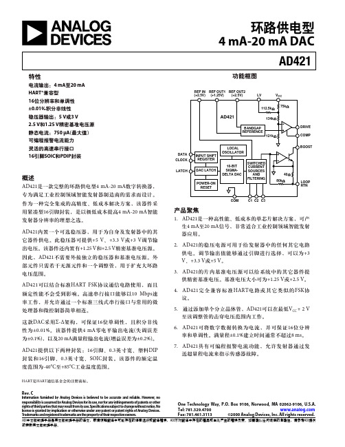
这款DAC采用Σ-Δ架构,可保证16位单调性,且积分非线 性为±0.01%。该器件提供4 mA零电平输出电流(失调误差 为±0.1%),以及20 mA满量程输出电流(增益误差为±0.2%)。
单位
条件/注释
精度 分辨率 单调性 积分非线性 失调(4 mA)(+25°C时)4 失调漂移 典型输出误差(20 mA) (+25°C时)4 总输出漂移 VCC电源灵敏度
16 16 ± 0.01 ± 0.1 ± 25 ± 0.2 ± 50 50
位 位(最小值) % FS(最大值) % FS(最大值) ppm FS/°C(最大值) % FS(最大值) ppm FS/°C(最大值) nA/mV(最大值)
FS = 满量程输出电流 VCC = 5 V 包括片内基准电压漂移 VCC = 5 V 包括片内基准电压漂移 25 nA/mV(典型值)
基准电压源 REF OUT2 输出电压 温漂
外部电流 VCC电源灵敏度 输出阻抗 噪声(0.1 Hz–10 Hz) REF OUT1
输出电压 温漂
外部电流 VCC电源灵敏度 输出阻抗 噪声(0.1 Hz–10 Hz) REF IN 输入电阻
7. AD421具有可编程报警电流功能,允许发射器通过发 送超量程电流来指示传感器故障。
HART是HART通信基金会的注册商标。
Rev. C
Information furnished by Analog Devices is believed to be accurate and reliable. However, no responsibility is assumed by Analog Devices for its use, nor for any infringements of patents or other rightsofthirdpartiesthatmayresultfromitsuse.Speci cationssubjecttochangewithoutnotice.No license is granted by implication or otherwise under any patent or patent rights of Analog Devices. Trademarks and registered trademarks are the property of their respective owners.
低偏移,1到4 LVCMOS LVTTL到3.3V LVPECL分频缓冲器 ICS8535-01说明
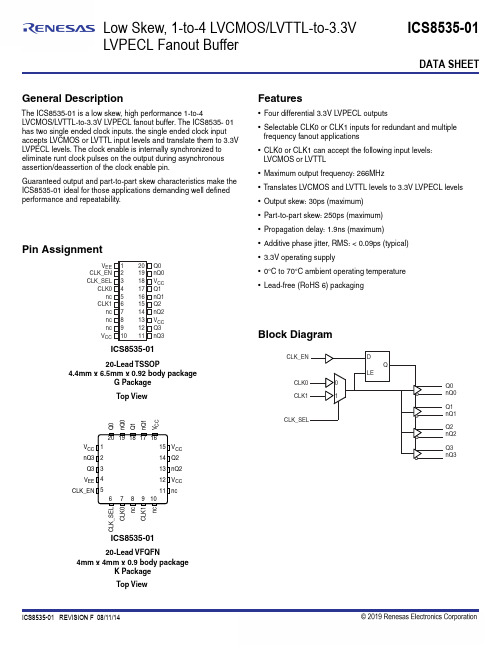
Low Skew, 1-to-4 LVCMOS/LVTTL-to-3.3V LVPECL Fanout BufferICS8535-01General DescriptionThe ICS8535-01is a low skew,high performance 1-to-4LVCMOS/LVTTL-to-3.3V LVPECL fanout buffer.The ICS8535-01has two single ended clock inputs.the single ended clock input accepts LVCMOS or LVTTL input levels and translate them to 3.3V LVPECL levels.The clock enable is internally synchronized to eliminate runt clock pulses on the output during asynchronous assertion/deassertion of the clock enable pin.Guaranteed output and part-to-part skew characteristics make the ICS8535-01ideal for those applications demanding well defined performance and repeatability.6 7 89 1019 20 18 17 1612345V CC Q2nQ2V CC nc1314151211Q3nQ3V CC V EE CLK_ENQ 0n Q 0Q 1n Q 1V C Cn cC L K 0C L K _S E LC L K 1n c12345678910Q0nQ0V CC Q1nQ1Q2nQ2V CC Q3nQ320191817161514131211V EE CLK_EN CLK_SELCLK0nc CLK1nc nc nc V CCICS8535-0120-Lead VFQFN4mm x 4mm x 0.9body packageK PackageTop ViewICS8535-0120-Lead TSSOP4.4mm x 6.5mm x 0.92body packageG PackageTop ViewPin AssignmentFeatures•Four differential 3.3V LVPECL outputs•Selectable CLK0or CLK1inputs for redundant and multiple frequency fanout applications•CLK0or CLK1can accept the following input levels:LVCMOS or LVTTL•Maximum output frequency:266MHz•T ranslates LVCMOS and LVTTL levels to 3.3V LVPECL levels •Output skew:30ps (maximum)•Part-to-part skew:250ps (maximum)•Propagation delay:1.9ns (maximum)•Additive phase jitter,RMS:<0.09ps (typical)•3.3V operating supply•0°C to 70°C ambient operating temperature •Lead-free (RoHS 6)packagingBlock DiagramICS8535-01 DATA SHEETPin Descriptions and CharacteristicsTable 1.Pin Descriptions 1Table 2.Pin CharacteristicsICS8535-01 DATA SHEETFigure 1.Table 3A.Control Input Function TableCLK0, CLK1CLK_ENnQ0:nQ3Q0:Q3Table 3B.Clock Input Function TableICS8535-01 DATA SHEETAbsolute Maximum RatingsNOTE:Stresses beyond those listed under Absolute Maximum Ratings may cause permanent damage to the device.These ratings are stress specifications only.Functional operation of product at these conditions or any conditions beyond those listed in the DC Electrical Characteristics or AC Characteristics is not implied.Exposure to absolute maximum rating conditions for extended periods may affect product reliability.DC Electrical CharacteristicsTable 4A.Power Supply DC Characteristics,V CC =3.3V±5%,T A =0°C to 70°CTable 4B.LVCMOS/LVTTL DC Characteristics,V CC =3.3V±5%,T A =0°C to 70°CTable 4C.LVPECL DC Characteristics,V CC =3.3V±5%,T A =0°C to 70°CCCICS8535-01 DATA SHEETAC CharacteristicsTable5.AC Characteristics,V CC =3.3V±5%,T A =0°C to 70°C 1The part does not add jitter.NOTE 2:Measured from the V CC /2of the input to the differential output crosspoint.NOTE 3:Defined as skew between outputs at the same supply voltage and with equal load conditions.Measured at the output differentialcrosspointsNOTE 4:This parameter is defined in accordance with JEDEC Standard 65.NOTE 5:Defined as skew between outputs on different devices operating at the same supply voltages and with equal load ingthe same type of inputs on each device,the outputs are measured at the differential crosspoints.NOTE 6:Driving only one input clock.ICS8535-01 DATA SHEETAdditive Phase JitterThe spectral purity in a band at a specific offset from the fundamental compared to the power of the fundamental is called the dBc Phase Noise.This value is normally expressed using a Phase noise plot and is most often the specified plot in many applications.Phase noise is defined as the ratio of the noise power present in a 1Hz band at a specified offset from the fundamental frequency to the power value of the fundamental.This ratio is expressed in decibels (dBm)or a ratioof the power in the 1Hz band to the power in the fundamental.When the required offset is specified,the phase noise is called a dBc value,which simply means dBm at a specified offset from the fundamental.By investigating jitter in the frequency domain,we get a betterunderstanding of its effects on the desired application over the entire time record of the signal.It is mathematically possible to calculate an expected bit error rate given a phase noise plot.As with most timing specifications,phase noise measurements have issues.The primary issue relates to the limitations of the equipment.Often the noise floor of the equipment is higher than the noise floorof the device.This is illustrated above.The device meets the noise floor of what is shown,but can actually be lower.The phase noise is dependent on the input source and measurement equipment.N o i s e P o w e r (d B c /H z )Offset Frequency (Hz)Input/Output Additive Phase Jitter at 156.25MHz =0.09ps (typical)1k10k100k1M10M-190-180-170-160-150-140-130-120-110-100-90-80-70-60-50-40-30-20-100100MICS8535-01 DATA SHEET Parameter MeasurementInformation3.3V Output Load Test CircuitOutput SkewPropagation DelayPart-to-Part SkewOutput Rise/Fall TimeOutput Duty Cycle/Pulse Width/PeriodICS8535-01 DATA SHEETApplications InformationRecommendations for Unused Input PinsInputs:CLK InputFor applications not requiring the use of a clock input,it can be left floating.Though not required,but for additional protection,a 1k Ωresistor can be tied from the CLK input to ground.LVCMOS Control PinsAll control pins have internal pullups;additional resistance is not required but can be added for additional protection.A 1k Ωresistor can be used.Outputs:LVPECL OutputsAll unused LVPECL outputs can be left floating.We recommend that there is no trace attached.Both sides of the differential output pair should either be left floating or terminated.Termination for 3.3V LVPECL OutputsThe clock layout topology shown below is a typical termination for LVPECL outputs.The two different layouts mentioned are recommended only as guidelines.The differential output is a low impedance follower output thatgenerate ECL/LVPECL compatible outputs.Therefore,terminating resistors (DC current path to ground)or current sources must be used for functionality.These outputs are designed to drive 50Ωtransmission lines.Matched impedance techniques should be used to maximize operating frequency and minimize signal distortion.Figure 2A and Figure 2B show two different layouts which arerecommended only as guidelines.Other suitable clock layouts may exist and it would be recommended that the board designerssimulate to guarantee compatibility across all printed circuit and clock component process variations.Figure 2A.3.3V LVPECL Output Termination Figure 2B.3.3V LVPECL Output TerminationICS8535-01 DATA SHEETSchematic ExampleFigure 3shows a schematic example of the ICS8535-01.In this example,the CLK0input is selected.The decoupling capacitors should be physically located near the power pin.For ICS8535-01,the unused clock outputs can be left floating.Figure 3.ICS8535-01Schematic ExampleICS8535-01 DATA SHEETPower ConsiderationsThis section provides information on power dissipation and junction temperature for the ICS8535-01.Equations and example calculations are also provided.1.Power Dissipation.The total power dissipation for the ICS8535-01is the sum of the core power plus the power dissipated in the load(s).The following is the power dissipation for V CC =3.3V +5%=3.465V ,which gives worst case results.NOTE:Please refer to Section 3for details on calculating power dissipated in the load.•Power (core)MAX =V CC_MAX *I EE_MAX =3.465V *50mA =173.25mW •Power (outputs)MAX =30mW/Loaded Output pairIf all outputs are loaded,the total power is 4*30mW =120mWTotal Power_MAX (3.465V ,with all outputs switching)=173.25mW +120mW =293.25mW 2.Junction Temperature.Junction temperature,Tj,is the temperature at the junction of the bond wire and bond pad and directly affects the reliability of the device.The maximum recommended junction temperature is 125°C.The equation for Tj is as follows:Tj =θJA *Pd_total +T A Tj =Junction T emperatureθJA =Junction-to-Ambient Thermal ResistancePd_total =T otal Device Power Dissipation (example calculation is in section 1above)T A =Ambient T emperatureIn order to calculate junction temperature,the appropriate junction-to-ambient thermal resistance θJA must be used.Assuming a moderate air flow of 200linear feet per minute and a multi-layer board,the appropriate value is 66.6°C/W per T able 6A below.Therefore,Tj for an ambient temperature of 70°C with all outputs switching is:70°C +0.293W *66.6°C/W =89.5°C.This is below the limit of 125°C.This calculation is only an example.Tj will obviously vary depending on the number of loaded outputs,supply voltage,air flow and the type of board (single layer or multi-layer).Table 6A.Thermal Resistance θfor 20-Lead TSSOP ,Forced ConvectionNOTE:Most modern PCB designs use multi-layered boards.The data in the second row pertains to most designs.Table 6B.θvs.Air Flow Table for 20-Lead VFQFNICS8535-01 DATA SHEET 3.Calculationsand Equations.The purpose of this section is to derive the power dissipated into the load.LVPECL output driver circuit and termination are shown in Figure4.Figure4.LVPECL Driver Circuit and TerminationT o calculate worst case power dissipation into the load,use the following equations which assume a50Ωload,and a termination voltage of V CC–2V.•For logic high,V OUT=V OH_MAX=V CC_MAX–0.9V(V CC_MAX–V OH_MAX)=0.9V•For logic low,V OUT=V OL_MAX=V CO_MAX–1.7V(V CC_MAX–V OL_MAX)=1.7VPd_H is power dissipation when the output drives high.Pd_L is the power dissipation when the output drives low.Pd_H=[(V OH_MAX–(V CC_MAX–2V))/R L]*(V CC_MAX–V OH_MAX)=[(2V-(V CC_MAX–V OH_MAX))/R L]*(V CC_MAX–V OH_MAX)=[(2V-0.9V)/50Ω]*0.9V=19.8mWPd_L=[(V OL_MAX–(V CC_MAX–2V))/R L]*(V CC_MAX–V OL_MAX)=[(2V–(V CC_MAX–V OL_MAX))/R L]*(V CC_MAX–V OL_MAX)=[(2V–1.7V)/50Ω]*1.7V=10.2mWT otal Power Dissipation per output pair=Pd_H+Pd_L=30mWICS8535-01 DATA SHEETReliability InformationNOTE:Most modern PCB designs use multi-layered boards.The data in the second row pertains to most designs.Table 7B.θvs.Air Flow Table for 20-Lead VFQFNTransistor CountThe transistor count for the IS8535-01is 412.Table 7A.θJA vs.Air Flow Table for a 20-Lead TSSOPICS8535-01 DATA SHEETPackage Outline and Package DimensionsICS8535-01 DATA SHEETPackage Outline and Package Dimensions (continued)Package Outline -K Suffix for 20-Lead VFQFNReference Document:JEDEC Publication 95,MO-220NOTE:The drawing and dimension data originate from IDT package outline drawing PSC-4170,rev03.1.Dimensions and tolerances conform to ASME Y14.5M-19942.All dimensions are in millimeters.All angles are in degrees.3.N is the total number of terminals.4.All specifications comply with JEDEC MO-220.Table 9.Package Dimensions for 20-Lead VFQFNICS8535-01 DATA SHEETOrdering InformationTable10.Ordering InformationICS8535-01 DATA SHEETRevision History SheetICS8535-01 DATA SHEETDISCLAIMER Integrated Device Technology, Inc. (IDT) and its subsidiaries reserve the right to modify the products and/or specifications described herein at any time and at IDT’s sole discretion. All information in this document, including descriptions of product features and performance, is subject to change without notice. Performance specifications and the operating parameters of the described products are determined in the independent state and are not guaranteed to perform the same way when installed in customer products. The information contained herein is provided without representation or warranty of any kind, whether express or implied, including, but not limited to, the suitability of IDT’s products for any particular purpose, an implied warranty of merchantability, or non-infringement of the intellectual property rights of others. This document is presented only as a guide and does not convey any license under intellectual property rights of IDT or any third parties.IDT’s products are not intended for use in applications involving extreme environmental conditions or in life support systems or similar devices where the failure or malfunction of an IDT product can be reasonably expected to significantly affect the health or safety of users. Anyone using an IDT product in such a manner does so at their own risk, absent an express, written agreement by IDT.While the information presented herein has been checked for both accuracy and reliability, Integrated Device Technology (IDT) assumes no responsibility for either its use or for the infringement of any patents or other rights of third parties, which would result from its use. No other circuits, patents, or licenses are implied. This product is intended for use in normal commercial applications. Any other applications, such as those requiring extended temperature ranges, high reliability or other extraordinary environmental requirements are not recommended without additional processing by IDT. IDT reserves the right to change any circuitry or specifications without notice. IDT does not authorize or warrant any IDT product for use in life support devices or critical medical instruments.Corporate Headquarters6024 Silver Creek Valley Road San Jose, CA 95138 USASales1-800-345-7015 or 408-284-8200 Fax: Tech Supportemail:**************Corporate HeadquartersTOYOSU FORESIA, 3-2-24 Toyosu,Koto-ku, Tokyo 135-0061, Japan Contact InformationFor further information on a product, technology, the most up-to-date version of a document, or your nearest sales office, please visit:/contact/TrademarksRenesas and the Renesas logo are trademarks of Renesas Electronics Corporation. All trademarks and registered trademarks are the property of their respective owners.IMPORTANT NOTICE AND DISCLAIMERRENESAS ELECTRONICS CORPORATION AND ITS SUBSIDIARIES (“RENESAS”) PROVIDES TECHNICAL SPECIFICATIONS AND RELIABILITY DATA (INCLUDING DATASHEETS), DESIGN RESOURCES (INCLUDINGREFERENCE DESIGNS), APPLICATION OR OTHER DESIGN ADVICE, WEB TOOLS, SAFETY INFORMATION, AND OTHER RESOURCES “AS IS” AND WITH ALL FAULTS, AND DISCLAIMS ALL WARRANTIES, EXPRESS OR IMPLIED, INCLUDING, WITHOUT LIMITATION, ANY IMPLIED WARRANTIES OF MERCHANTABILITY, FITNESS FOR A PARTICULAR PURPOSE, OR NON-INFRINGEMENT OF THIRD PARTY INTELLECTUAL PROPERTY RIGHTS.These resources are intended for developers skilled in the art designing with Renesas products. You are solely responsible for (1) selecting the appropriate products for your application, (2) designing, validating, and testing your application, and (3) ensuring your application meets applicable standards, and any other safety, security, or other requirements. These resources are subject to change without notice. Renesas grants you permission to use these resources only for development of an application that uses Renesas products. Other reproduction or use of these resources is strictly prohibited. No license is granted to any other Renesas intellectual property or to any third party intellectual property. Renesas disclaims responsibility for, and you will fully indemnify Renesas and its representatives against, any claims,damages, costs, losses, or liabilities arising out of your use of these resources. Renesas' products are provided only subject to Renesas' Terms and Conditions of Sale or other applicable terms agreed to in writing. No use of any Renesas resources expands or otherwise alters any applicable warranties or warranty disclaimers for these products.(Rev.1.0 Mar 2020)。
稳压管大全)
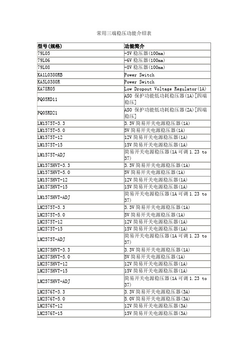
3.3V简易开关电源稳压器(1A)
LM1575T-5.0
5V简易开关电源稳压器(1A)
LM1575T-12
12V简易开关电源稳压器(1A)
LM1575T-15
15V简易开关电源稳压器(1A)
LM1575T-ADJ
简易开关电源稳压器(1A可调1.23 to 37)
LM1575HVT-3.3
LM2575HVT-ADJ
简易开关电源稳压器(1A可调1.23 to 37)
LM2576T-3.3
3.3V简易开关电源稳压器(3A)
LM2576T-5.0
5.0V简易开关电源稳压器(3A)
LM2576T-12
12V简易开关电源稳压器(3A)
LM2576T-15
15V简易开关电源稳压器(3A)
LM2576T-ADJ
79L08
-8V稳压器(100ma)
KA1L0380RB
Power Switch
KA5L0380R
Power Switch
KA78R05
Low Dropout Voltage Regulator(1A)
PQ05RD11
ASO保护功能低功耗稳压器(1A)[四端稳压]
PQ05RD21
ASO保护功能低功耗稳压器(2A)[四端稳压]
型号(规格)
功能简介
兼容型号
CA3130
高输入阻抗运算放大器
Intersil[DATA]
CA3140
高输入阻抗运算放大器
CD4573
四可编程运算放大器
MC14573
ICL7650
斩波稳零放大器
LF347(NS[DATA])
带宽四运算放大器
- 1、下载文档前请自行甄别文档内容的完整性,平台不提供额外的编辑、内容补充、找答案等附加服务。
- 2、"仅部分预览"的文档,不可在线预览部分如存在完整性等问题,可反馈申请退款(可完整预览的文档不适用该条件!)。
- 3、如文档侵犯您的权益,请联系客服反馈,我们会尽快为您处理(人工客服工作时间:9:00-18:30)。
货币霸主地位的形成,除了经济作为决定性因素,还有就是必须具备相应的历史条件。
人民币要获得霸主地位,必须具备三个条件:首先,中国必须成为全球唯一的经济强国,这至少还需要一百年的时间。
其次,中国必须成为全球创新力最强的国家。
目前中
包括政治、经济、文化、教育和科技等各个领域的创新机制的形成。
第三,必须具备相应的时机。
从目前来
看,由于中国的经济实力不及,这个机会只能眼睁睁看着从我们身边溜过。
除此,如果发达国家经济出现了大的衰退,新一轮科技革命又发生在中国,这也可能是一个难得的机会。
总之,一旦具备了这些条件,人民币称霸世界则是一种必然。
现在,就让我们来看看一国货币是如何称霸世界以及全球货币霸主地位是如何更替的。
世人皆知,
英镑之所以能够称霸世界,其根本原因是工业
国,加之其在全球推行殖民主义,推动英镑在人类历史上首次成为全球货币的霸主。
然而,后来英镑的霸主地位受到了挑战,特别是随着美国经济实力的增强,在1919至1939年期间,美元已
经与英镑并驾齐驱,二战的暴发却为美元独自称霸世界创造了条件。
本博主以为,只有当中国的复兴结束而成为世界唯一的经济强国,人民币才有称霸全球的可能。
当这个可能开始变为现实的时候,人民币还将与美元共同称霸世界一段时间之后,人民币才能获得全球货币的唯一霸主地位。
越来越强,其原因就在于人民币的国际化是中国经济发展的客观需要。
当人民币能够跨越国界,在境外流通,成为国际上普遍认可的计价、结算及
储备货币时,中国也就进入了一个新的复兴阶段。
但人民币的国际化并不意味其霸主地位的形成。
那么,人民币有称霸世界的可能吗?
在人类历史上,只有两种货币称霸世界,一是英镑,二是美元,这也决定了全球货币霸主地位只进行过一次更替,那就是美元取代英镑而称霸世界至今。
1939年以后,随着英国在二战战场上节节败退,美国却借机大发战争财,一下超越了英国,尤其是二战结束以后,美国的经济实力达到顶峰,成为全球唯一的经济强国,由于英国等欧洲国家面临着战后重建,资金非常短缺,不得不求助于美国。
此时,聪明的美国人乘机建立布雷顿森林体系,美元直接与黄金挂钩,各国货币则与美元挂钩,并以金本位为基础建立新的国际汇率和贸
易体系。
元纸币,形成了以美元为中心的循环,欧洲各国之间也开始用美元进行结算,由此推动了美元作为全球唯一货币霸主地位的形成。
后来,由于美国成为全球科技与金融创新力最强大的国家,尽管遭遇了许多坎坷,但并没有动摇美元的霸主地位。