LV5217GP-TE-L-E;中文规格书,Datasheet资料
[整理]REX521技术参考手册.
![[整理]REX521技术参考手册.](https://img.taocdn.com/s3/m/a7848f756bd97f192279e9f9.png)
REX 521型微机保护继电器技术参考手册汇编上海ABB工程有限公司2002,08,181. 概述REX521建立在RED500平台上,是REF54_型馈线终端的一种简化产品。
它是综合保护、控制、测量、监视和通信为一体的微机终端。
本手册阐述REX521终端的概貌、及其配置。
首先是概述,第二部分逐项描述了基本配置和中级配置等两种的标准配置的概况,第三部分到第六部分介绍了信号路径及其功能,第七部分为应用举例。
最后是附录,为原版Copy的技术数据和外部结线图,以供查阅防止误导。
REX 521 和RED 500 平台在功能模块介绍上的不同在CD-ROM“功能的技术介绍” (1MRS 750889-MUM)的功能模块的介绍方面, REX521 和RED 500 平台在某些方面有所不同。
首先,某些术语是指其他产品而不是REX521,其次,有某些数据仅适用于REX521:• 在试验某一功能模块时,READY 指示灯闪烁。
• 事件标识位1仅适用于SPA 通讯。
• 不能实现直接控制自动重合闸的功能。
REX521输入、输出量一览表:REX521的输出继电器接点能力REX521 机箱安装尺寸:请参阅下图中的标准19英寸的1/3 (表中第二项)。
REX521的整定范围一览表:REX521的通信串口:面前一个背后两个,全是光纤通信口。
背后串口的通信规约LON/IEC/SPA 可选。
表1.-1 REX 521的两种标准配置表1.-2 REX521的保护功能表1.-3 REX521的控制功能表 1.-4 REX521的测量功能表 1.-5 REX 521的状态监测功能表 1.-6 REX 521电源质量监视功能基本配置和中级配置的主要区别在于,中级配置增加了方向接地保护。
B01和B02以及M01和 M02之间的区别是,B02 和M02增加了自动重合闸功能。
2. 信号路径总图表示除模拟量信号外的输入、输出的功能控制的耒龙去脉的信号路径图图:2.-1 信号路径总图概念2.1. 数字量输入为了实现不同的功能,数字量输入(DI1...DI9) 要连接到功能模块的输入口,或直接连接到输出回路。
EML17T2R;中文规格书,Datasheet资料

Transistors1/3General purpose transistor (isolated transistor and diode)EML17DTA144E and a RB520G-30 are housed independently in a EMT package.z ApplicationsDC / DC converter Motor driverz Features1) Tr : Degital Transistor Di : Low V F 2) Small packagez StructureSilicon epitaxial planar degital transistor Schottky barrier diodez External dimensions (Unit : mm)z Equivalent circuitz Packaging specificationsType EML17EMT5L17T2R 8000Package Marking CodeBasic ordering unit (pieces)Transistors 2/3z Absolute maximum ratings (T a=25°C) Tr2Parameter Symbol V CC V IN I O I C(MAX)TjLimits −50−40 to +10−30−100150Unit V V mA °CSupply voltage Input voltage Output current Junction temperaturePd 120mW Power dissipationDi1, Tr2Parameter SymbolPd Tstg Limits150−55 to +125Unit mW ∗∗ Each terminal mounted on a recommended land.°CPower dissipationRange of storage temperaturez Electrical characteristics (T a=25°C) Di1ParameterSymbol Min.Typ.Max.Unit Conditions−0.45V F −V I F =10mA V R =10VForward voltage I R−−0.5µAReverse current∗ Please pay attention to static electricity when handling.Tr2ParameterSymbol Min.Typ.Max.Unit ConditionsV CE = −10V, I E =5mA, f =100MHz∗∗ Transition frequency of the deviceResistance ratio R 2/R 10.81 1.2−−V I(off)−−−0.5I C = −5V, I O = −100µA Input voltage V I(on)−3.0−−V V O = −0.3V, I O = −2mA V O(on)−−0.1−0.3V I O /I I = −10mA/ −0.5mA Output voltage I I −−−0.18mA V I = −5VInput current I O(off)−−−0.5µA V CC = −50V, V I =0V Output current G 168−−−V O = −5V, I O = −5mADC current gain R 132.94761.1k Ω−Input resistance f T −250−MHz Transition frequencyTransistors 3/3z Electrical characteristic curves Di1R E V E R S E C U R R E N T : I R (n A )REVERSE VOLTAGE : V R (V)Fig.2 Reverse characteristicsF O R W A R D C U R R E N T : I F (m A )FORWARD VOLTAGE : V F (mV)Fig.1 Forward characteristics101525520110100REVERSE VOLTAGE : V R (V)C A P A C I T A N C E B E T W E E N T E R M I N A L S : C T (p F )Fig. 3 Capacitance between terminals characteristics30Tr2I N P U T V O L T A G E : V I (o n ) (V )OUTPUT CURRENT : I O (A)−−−−−−−−−−−Fig.4 Input voltage vs. output current (ON characteristics)−−1−−−−200−500−100−20−50−10−2−5INPUT VOLTAGE : V I(off) (V)O U T P U T C U R R E N T : I o (A )Fig.5 Output current vs. Input voltage (OFF characteristics)−D C C U R R E N T G A I N : G IOUTPUT CURRENT : I O (A)Fig.6 DC current gain vs. output current−−−−−−−−−−−OUTPUT CURRENT : I O (A)O U T P U T V O L T A G E : V O (o n ) (V )Fig.7 Output voltage vs. output currentAppendixAbout Export Control Order in JapanProducts described herein are the objects of controlled goods in Annex 1 (Item 16) of Export T rade ControlOrder in Japan.In case of export from Japan, please confirm if it applies to "objective" criteria or an "informed" (by MITI clause)on the basis of "catch all controls for Non-Proliferation of Weapons of Mass Destruction.Appendix1-Rev1.1分销商库存信息: ROHMEML17T2R。
W25Q128BVEIG;中文规格书,Datasheet资料

Publication Release Date: April 18, 20123V 128M-BITSERIAL FLASH MEMORY WITH DUAL AND QUAD SPITable of Contents1.GENERAL DESCRIPTION (5)2.FEATURES (5)3.PACKAGE TYPES AND PIN CONFIGURATIONS (6)3.1Pad Configuration WSON 8x6-mm (6)3.2Pad Description WSON 8x6-mm (6)3.3Pin Configuration SOIC 300-mil (7)3.4Pin Description SOIC 300-mil (7)3.5Ball Configuration TFBGA 8x6-mm (5x5 or 6x4 Ball Array) (8)3.6Ball Description TFBGA 8x6-mm (8)4.PIN DESCRIPTIONS (9)4.1Chip Select (/CS) (9)4.2Serial Data Input, Output and IOs (DI, DO and IO0, IO1, IO2, IO3) (9)4.3Write Protect (/WP) (9)4.4HOLD (/HOLD) (9)4.5Serial Clock (CLK) (9)5.BLOCK DIAGRAM (10)6.FUNCTIONAL DESCRIPTIONS (11)6.1SPI OPERATIONS (11)6.1.1Standard SPI Instructions (11)6.1.2Dual SPI Instructions (11)6.1.3Quad SPI Instructions (11)6.1.4Hold Function (11)6.2WRITE PROTECTION (12)6.2.1Write Protect Features (12)7.STATUS REGISTERS AND INSTRUCTIONS (13)7.1STATUS REGISTERS (13)7.1.1BUSY Status (BUSY) (13)7.1.2Write Enable Latch Status (WEL) (13)7.1.3Block Protect Bits (BP2, BP1, BP0) (13)7.1.4Top/Bottom Block Protect Bit (TB) (13)7.1.5Sector/Block Protect Bit (SEC) (13)7.1.6Complement Protect Bit (CMP) (14)7.1.7Status Register Protect Bits (SRP1, SRP0) (14)7.1.8Erase/Program Suspend Status (SUS) (14)7.1.9Security Register Lock Bits (LB3, LB2, LB1) (14)7.1.10Quad Enable Bit (QE) (15)7.1.11Status Register Memory Protection (CMP = 0) (16)7.1.12 Status Register Memory Protection (CMP = 1) (17)Publication Release Date: April 18, 20127.2 INSTRUCTIONS (18)7.2.1 Manufacturer and Device Identification ................................................................................ 18 7.2.2 Instruction Set Table 1 (Erase, Program Instructions) .......................................................... 19 7.2.3 Instruction Set Table 2 (Read Instructions) .......................................................................... 20 7.2.4 Instruction Set Table 3 (ID, Security Instructions) ................................................................ 21 7.2.5 Write Enable (06h) ............................................................................................................... 22 7.2.6 Write Enable for Volatile Status Register (50h) .................................................................... 22 7.2.7 Write Disable (04h) ............................................................................................................... 23 7.2.8 Read Status Register-1 (05h) and Read Status Register-2 (35h) ........................................ 24 7.2.9 Write Status Register (01h) .................................................................................................. 24 7.2.10 Read Data (03h) ................................................................................................................. 26 7.2.11 Fast Read (0Bh) ................................................................................................................. 27 7.2.12 Fast Read Dual Output (3Bh) ............................................................................................. 28 7.2.13 Fast Read Quad Output (6Bh) ............................................................................................ 29 7.2.14 Fast Read Dual I/O (BBh) ................................................................................................... 30 7.2.15 Fast Read Quad I/O (EBh) ................................................................................................. 32 7.2.16 Word Read Quad I/O (E7h) ................................................................................................ 34 7.2.17 Octal Word Read Quad I/O (E3h) ....................................................................................... 36 7.2.18 Set Burst with Wrap (77h) .................................................................................................. 38 7.2.19 Continuous Read Mode Bits (M7-0) ................................................................................... 39 7.2.20 Continuous Read Mode Reset (FFh or FFFFh) .................................................................. 39 7.2.21 Page Program (02h) ........................................................................................................... 40 7.2.22 Quad Input Page Program (32h) ........................................................................................ 41 7.2.23 Sector Erase (20h) ............................................................................................................. 42 7.2.24 32KB Block Erase (52h) ..................................................................................................... 43 7.2.25 64KB Block Erase (D8h) ..................................................................................................... 44 7.2.26 Chip Erase (C7h / 60h) ....................................................................................................... 45 7.2.27 Erase / Program Suspend (75h) ......................................................................................... 46 7.2.28 Erase / Program Resume (7Ah) ......................................................................................... 47 7.2.29 Power-down (B9h) .............................................................................................................. 48 7.2.30 Release Power-down / Device ID (ABh) ............................................................................. 49 7.2.31 Read Manufacturer / Device ID (90h) ................................................................................. 51 7.2.32 Read Manufacturer / Device ID Dual I/O (92h) ................................................................... 52 7.2.33 Read Manufacturer / Device ID Quad I/O (94h) ................................................................. 53 7.2.34 Read Unique ID Number (4Bh)........................................................................................... 54 7.2.35 Read JEDEC ID (9Fh) ........................................................................................................ 55 7.2.36 Read SFDP Register (5Ah) ................................................................................................ 56 7.2.37 Erase Security Registers (44h) ........................................................................................... 57 7.2.38 Program Security Registers (42h) ...................................................................................... 58 7.2.39 Read Security Registers (48h) . (59)8.ELECTRICAL CHARACTERISTICS (60)8.1Absolute Maximum Ratings (60)8.2Operating Ranges (60)8.3Power-up Timing and Write Inhibit Threshold (61)8.4DC Electrical Characteristics (62)8.5AC Measurement Conditions (63)8.6AC Electrical Characteristics (64)8.7AC Electrical Characteristics (cont’d) (65)8.8Serial Output Timing (66)8.9Serial Input Timing (66)8.10HOLD Timing (66)8.11WP Timing (66)9.PACKAGE SPECIFICATION (67)9.18-Pad WSON 8x6-mm (Package Code E) (67)9.216-Pin SOIC 300-mil (Package Code F) (68)9.324-Ball TFBGA 8x6-mm (Package Code B, 5x5-1 Ball Array) (69)9.424-Ball TFBGA 8x6-mm (Package Code C, 6x4 Ball Array) (70)10.ORDERING INFORMATION (71)10.1Valid Part Numbers and Top Side Marking (72)11.REVISION HISTORY (73)Publication Release Date: April 18, 20121. GENERAL DESCRIPTIONThe W25Q128BV (128M-bit) Serial Flash memory provides a storage solution for systems with limited space, pins and power. The 25Q series offers flexibility and performance well beyond ordinary Serial Flash devices. They are ideal for code shadowing to RAM, executing code directly from Dual/Quad SPI (XIP) and storing voice, text and data. The device operates on a single 2.7V to 3.6V power supply with current consumption as low as 4mA active and 1µA for power-down.The W25Q128BV array is organized into 65,536 programmable pages of 256-bytes each. Up to 256 bytes can be programmed at a time. Pages can be erased in groups of 16 (4KB sector erase), groups of 128 (32KB block erase), groups of 256 (64KB block erase) or the entire chip (chip erase). The W25Q128BV has 4,096 erasable sectors and 256 erasable blocks respectively. The small 4KB sectors allow for greater flexibility in applications that require data and parameter storage. (See Figure 2.)The W25Q128BV supports the standard Serial Peripheral Interface (SPI), and a high performance Dual/Quad output as well as Dual/Quad I/O SPI: Serial Clock, Chip Select, Serial Data I/O0 (DI), I/O1 (DO), I/O2 (/WP), and I/O3 (/HOLD). SPI clock frequencies of up to 104MHz are supported allowing equivalent clock rates of 208MHz (104MHz x 2) for Dual Output and 280MHz (70MHz x 4) for Quad SPI when using the Fast Read Quad SPI instructions. These transfer rates can outperform standard Asynchronous 8 and 16-bit Parallel Flash memories. The Continuous Read Mode allows for efficient memory access with as few as 8-clocks of instruction-overhead to read a 24-bit address, allowing true XIP (execute in place) operation.A Hold pin, Write Protect pin and programmable write protection, with top, bottom or complement array control, provide further control flexibility. Additionally, the device supports JEDEC standard manufacturer and device identification with a 64-bit Unique Serial Number.2. FEATURES• Family of SpiFlash Memories – W25Q128BV: 128M-bit/16M-byte – 256-byte per programmable page– Standard SPI: CLK, /CS, DI, DO, /WP, /Hold– Dual SPI: CLK, /CS, IO 0, IO 1, /WP, /Hold– Quad SPI: CLK, /CS, IO 0, IO 1, IO 2, IO 3• Highest Performance Serial Flash– 104/70MHz Dual Output/Quad SPI clocks– 208/280MHz equivalent Dual /Quad SPI– 35MB/S continuous data transfer rate– Up to 5X that of ordinary Serial Flash– More than 100,000 erase/program cycles (1)– More than 20-year data retention• Efficient “Continuous Read Mode” – Low Instruction overhead– Continuous Read with 8/16/32/64-Byte Wrap – As few as 8 clocks to address memory – Allows true XIP (execute in place) operation – Outperforms X16 Parallel Flash • Low Power, Wide Temperature Range– Single 2.7 to 3.6V supply– 4mA active current, <1µA Power-down current – -40°C to +85/105°C operating range • Flexible Architecture with 4KB sectors– Uniform Sector/Block Erase (4K/32K/64K-Byte)– Program one to 256 bytes– Erase/Program Suspend & Resume• Advanced Security Features – Software and Hardware Write-Protect – Top/Bottom, 4KB complement array protection – Lock-Down and OTP array protection – 64-Bit Unique Serial Number for each device – Discoverable Parameters (SFDP) Register – 3X256-Byte Security Registers with OTP locks– Volatile & Non-volatile Status Register Bits• Space Efficient Packaging – 8-pad WSON 8x6-mm – 16-pin SOIC 300-mil – 24-ball TFBGA 8x6-mm– Contact Winbond for KGD and other options Note 1. More than 100k Block Erase/Program cycles for Industrial and Automotive temperature; more than 10k fullchip Erase/Program cycles tested in compliance with AEC-Q100.3.PACKAGE TYPES AND PIN CONFIGURATIONSW25Q128BV is offered in an 8-pad WSON 8x6-mm (package code E), a 16-pin SOIC 300-mil (package code F) and two 24-ball 8x6-mm TFBGAs (package code B, C) as shown in Figure 1a-c respectively. Package diagrams and dimensions are illustrated at the end of this datasheet.3.1Pad Configuration WSON 8x6-mmFigure 1a. W25Q128BV Pad Assignments, 8-pad WSON 8x6-mm (Package Code E)3.2Pad Description WSON 8x6-mmPAD NO. PAD NAME I/O FUNCTION1 /CS I Chip Select Input2 DO (IO1) I/O Data Output (Data Input Output 1)*1(IO2)I/O Write Protect Input ( Data Input Output 2)*23 /WP4 GND Ground5 DI (IO0) I/O Data Input (Data Input Output 0)*16 CLK I Serial Clock Input(IO3)I/O Hold Input (Data Input Output 3)*27 /HOLD8 VCC PowerSupply*1: IO0 and IO1 are used for Standard and Dual SPI instructions*2: IO0 – IO3 are used for Quad SPI instructionsPublication Release Date: April 18, 20123.3 Pin Configuration SOIC 300-milFigure 1b. W25Q128BV Pin Assignments, 16-pin SOIC 300-mil (Package Code F)3.4 Pin Description SOIC 300-milPIN NO.PIN NAMEI/OFUNCTION1 /HOLD (IO3)I/OHold Input (Data Input Output 3)*22 VCC Power Supply3 N/C No Connect4 N/C No Connect5 N/C No Connect6 N/C No Connect7 /CS I Chip Select Input8DO (IO1)I/O Data Output (Data Input Output 1)*19 /WP (IO2)I/OWrite Protect Input (Data Input Output 2)*210 GND Ground 11 N/C No Connect 12 N/C No Connect 13 N/C No Connect 14 N/C No Connect 15 DI (IO0) I/O Data Input (Data Input Output 0)*116CLKISerial Clock Input*1: IO0 and IO1 are used for Standard and Dual SPI instructions.*2: IO0 – IO3 are used for Quad SPI instructions, /WP or /HOLD functions are only available for Standard/Dual SPI.3.5Ball Configuration TFBGA 8x6-mm (5x5 or 6x4 Ball Array)Figure 1c. W25Q128BV Ball Assignments, 24-ball TFBGA 8x6-mm (Package Code B, C)3.6Ball Description TFBGA 8x6-mmBALL NO. PIN NAME I/O FUNCTIONB2 CLK I Serial Clock InputB3 GND GroundSupplyB4 VCC PowerC2 /CS I Chip Select Input(IO2)I/O Write Protect Input (Data Input Output 2)*2C4 /WPD2 DO (IO1) I/O Data Output (Data Input Output 1)*1D3 DI (IO0) I/O Data Input (Data Input Output 0)*1(IO3)I/O Hold Input (Data Input Output 3)*2D4 /HOLDMultiple NC NoConnect*1: IO0 and IO1 are used for Standard and Dual SPI instructions.*2: IO0 – IO3 are used for Quad SPI instructions, /WP or /HOLD functions are only available for Standard/Dual SPI.Publication Release Date: April 18, 20124. PIN DESCRIPTIONS4.1 Chip Select (/CS)The SPI Chip Select (/CS) pin enables and disables device operation. When /CS is high the device is deselected and the Serial Data Output (DO, or IO0, IO1, IO2, IO3) pins are at high impedance. When deselected, the devices power consumption will be at standby levels unless an internal erase, program or write status register cycle is in progress. When /CS is brought low the device will be selected, power consumption will increase to active levels and instructions can be written to and data read from the device. After power-up, /CS must transition from high to low before a new instruction will be accepted. The /CS input must track the VCC supply level at power-up (see “Write Protection” and Figure 38). If needed a pull-up resister on /CS can be used to accomplish this.4.2 Serial Data Input, Output and IOs (DI, DO and IO0, IO1, IO2, IO3)The W25Q128BV supports standard SPI, Dual SPI and Quad SPI operation. Standard SPI instructions use the unidirectional DI (input) pin to serially write instructions, addresses or data to the device on the rising edge of the Serial Clock (CLK) input pin. Standard SPI also uses the unidirectional DO (output) to read data or status from the device on the falling edge of CLK.Dual and Quad SPI instructions use the bidirectional IO pins to serially write instructions, addresses or data to the device on the rising edge of CLK and read data or status from the device on the falling edge of CLK. Quad SPI instructions require the non-volatile Quad Enable bit (QE) in Status Register-2 to be set. When QE=1, the /WP pin becomes IO2 and /HOLD pin becomes IO3.4.3 Write Protect (/WP)The Write Protect (/WP) pin can be used to prevent the Status Register from being written. Used in conjunction with the Status Register’s Block Protect (CMP, SEC, TB, BP2, BP1 and BP0) bits and Status Register Protect (SRP) bits, a portion as small as a 4KB sector or the entire memory array can be hardware protected. The /WP pin is active low. When the QE bit of Status Register-2 is set for Quad I/O, the /WP pin function is not available since this pin is used for IO2. See Figure 1a-c for the pin configuration of Quad I/O operation.4.4 HOLD (/HOLD)The /HOLD pin allows the device to be paused while it is actively selected. When /HOLD is brought low, while /CS is low, the DO pin will be at high impedance and signals on the DI and CLK pins will be ignored (don’t care). When /HOLD is brought high, device operation can resume. The /HOLD function can be useful when multiple devices are sharing the same SPI signals. The /HOLD pin is active low. When the QE bit of Status Register-2 is set for Quad I/O, the /HOLD pin function is not available since this pin is used for IO3. See Figure 1a-c for the pin configuration of Quad I/O operation.4.5 Serial Clock (CLK)The SPI Serial Clock Input (CLK) pin provides the timing for serial input and output operations. ("See SPI Operations")5.BLOCK DIAGRAM ArrayFigure 2. W25Q128BV Serial Flash Memory Block Diagram分销商库存信息: WINBONDW25Q128BVEIG。
18BISV0501 LV-HUB 产品说明书

Communication HUBLV-HUB Product ManualInformation Version: 2.2Pylon Technologies Co., Ltd.No. 73, Lane 887, ZuChongzhi Road, Zhangjiang Hi-Tech ParkPudong, Shanghai 201203, China Zip Code: 201203Fax:Email:Website: This manual introduces LV-Hub from Pylontech. LV-Hub is a communication hub for US2000/US3000 Lithium-Ion Phosphate Battery storage system.Please read this manual before you install the battery and follow the instruction carefully during the installation process.CONTENT1.INTRODUCTION (3)2.LV-HUB (3)2.1 PORTS: (4)2.2 DEFINITION OF RJ45 PORT PIN (5)2.3 LED INDICATORS INSTRUCTIONS (5)3.OPERATION (6)3.1 PROTOCOL (6)3.2 CABLES CONNECTION FOR US2000/US3000 UNDER RS485 OR CANBUS. (6)3.2.1 CABLES CONNECTION FOR RS485 (6)3.2.2 CABLES CONNECTION FOR CAN (SINGLE HUB) (7)3.3 CABLES CONNECTION FOR US2000C/US3000C/UP5000/US5000 UNDER CANBUS (8)3.4 CABLES CONNECTION FOR MULTIPLE HUBS UNDER CANBUS. (9)ANNEX 1: CABLES CONNECTION FOR US2000/US3000 UNDER RS485 (10)ANNEX 2: CABLES CONNECTION FOR US2000/US3000 UNDER CAN (11)ANNEX 3: CABLES CONNECTION FOR CAN (MULTI HUB) (12)ANNEX 4: CABLES CONNECTION FOR US2000C/US3000C/UP5000/US5000 UNDER CANBUS (13)1.IntroductionLV-Hub is the CAN/RS485 communication hub for multiple 48V battery groups in parallel connection.Fit Description: US2000 / US3000 / Phantom-SA / US1800.2.LV-Hub-A2.1 Ports:3.Operation3.1 ProtocolCAN: CAN-Bus-protocol-PYLON-low-voltage-V1.2-20180408 or above.RS485: RS485-protocol-pylon-low-voltage-V3.1-20180408 or above.3.2 Cables Connection for US2000/US3000 under RS485 or CANBUS.3.2.1 Cables Connection for RS485⚫Each battery group can configure maximum 8pcs US2000B Plus or 8pcs US3000.⚫LV-Hub-A configures maximum 5 group batteries.⚫RS485 communication needn’t additional cable and power just a simple hub is enough.⚫When each battery group’s current is >120A, this battery group must configure 2 pair external power cables like the diagram.⚫The details of ADD Switch setting also can see the menu of battery.3.2.2 Cables Connection for CAN (single HUB)⚫Each battery group can configure maximum 8pcs US2000B Plus or 8pcs US3000.⚫LV-Hub-A configures maximum 5 group batteries.⚫When each battery group’s current is >120A, this battery group must configure 2 pair external power cables like the diagram.⚫The details of ADD Switch setting also can see the menu of battery.⚫When using with SMA SUNNY ISLAND, the ADD on HUB(or master HUB if there are multiple HUBs) must be 000011(for B14V0105 presenting on product label) or 000101 (for B14V0106 presenting on product label).3.3 Cables Connection for US2000C/US3000C/UP5000/US5000 under CANBUSThe specific cable connection way please refer to the related battery operation manual.Connect power cable first:1) each pair of cable hold max 100A constant current. Connect enough pairs of cable based on calculationof system current.2) Suitable protection breaker between battery system and inverter is required.3) connect power cable of LV-HUB4) Make sure all dipswitch is X0XX, then turn ON batteries.5) After all batteries running and buzzer of master battery in group1 rings 3 times. Means all groups areonline.6) Change the dip switch of master battery in group1to X1XX. Then connect communication cablebetween LV-HUB and master battery in group 1.7) C hange the dip switch of LV-HUB to 000001, t hen turn on LV-HUB.*Below communication cable shall be 8 pin direct-pin cable:a. Between battery modulesb. Between LV-HUB Port 0 to LV-HUB CAN IN*Below communication cable shall has first 3 pin NULL or use WI0SCAN30RJ1 cable inside external cable kits:a. Between Group 1 Master Battery A/CAN to LV-HUB Port 1.Note: When using US2000C/US3000C/UP5000/US5000, the multiple group connection under RS485 communication DONOT require a LV-HUB. The wiring diagram please refer to the corresponding battery model operation manual.3.4 Cables Connection for Multiple HUBs under CANBUS.In above picture, all communication cable connect in between shall be 8 pin direct-pin cable.Annex 1: Cables Connection for US2000/US3000 under RS485Annex 2: Cables Connection for US2000/US3000 under CANAnnex 3: Cables Connection for CAN (multi HUB)Annex 4: Cables Connection for US2000C/US3000C/UP5000/US5000 under CANBUSPylon Technologies Co., Ltd.No. 73, Lane 887, ZuChongzhi Road, Zhangjiang Hi-Tech Park Pudong, Shanghai 201203, ChinaT +86-21-51317699 | F +86-21-51317698E *********************.cnW 。
proteus元件中英文对照表.

1.analog ics 模拟集成器件8个子类:amplifier 放大器comparators 比较器display drivers 显示驱动器filters 滤波器miscellaneous 混杂器件regulators 三端稳压器timers 555定时器voltage references 参考电压2,capacitors CAP电容,23个分类别animated 可显示充放电电荷电容audio grade axial 音响专用电容axial lead polypropene 径向轴引线聚丙烯电容axial lead polystyrene 径向轴引线聚苯乙烯电容ceramic disc 陶瓷圆片电容decoupling disc 解耦圆片电容high temp radial 高温径向电容high temp axial electrolytic高温径向电解电容metallised polyester film 金属聚酯膜电容metallised polypropene 金属聚丙烯电容metallised polypropene film 金属聚丙烯膜电容miniture electrolytic 微型电解电容multilayer metallised polyester film 多层金属聚酯膜电容mylar film 聚酯薄膜电容nickel barrier 镍栅电容non polarised 无极性电容polyester layer 聚酯层电容radial electrolytic 径向电解电容resin dipped 树脂蚀刻电容tantalum bead 钽珠电容variable 可变电容vx a xial electrolytic VX 轴电解电容3,CMOS 4000 series 4000系列数字电路adders 加法器buffers & drivers 缓冲和驱动器comparators 比较器counters 计数器decoders 译码器encoders 编码器flip-flops & latches 触发器和锁存器frequency dividers & tiner 分频和定定时器gates & inverters 门电路和反相器memory 存储器misc.logic 混杂逻辑电路mutiplexers 数据选择器multivibrators 多谐振荡器phase-locked loops(PLL) 锁相环registers 寄存器signal switcher 信号开关4,connectors 接头;8个分类:audio 音频接头D-type D型接头DIL 双排插座header blocks 插头miscellaneous 各种接头PCB transfer PCB 传输接头SIL 单盘插座ribbon cable 蛇皮电缆terminal blocks 接线端子台5,data converters 数据转换器:4个分类:A/D converters 模数转换器D/A converters 数模转换器sample & hold 采样保持器temperature sensors 温度传感器6,debugging tools 调试工具数据:3个类别:breakpoint triggers 断点触发器logic probes 逻辑输出探针logic timuli 逻辑状态输入7,diodes 二极管;8个分类:bridge rectifiers 整流桥generic 普通二极管rectifiers 整流二极管schottky 肖特基二极管switching 开关二极管tunnel 隧道二极管varicap 稳压二极管8,inductors 电感:3个类别:generic 普通电感SMT inductors 表面安装技术电感transformers 变压器9,laplace primitives 拉普拉斯模型:7个类别:1st order 一阶模型2nd order 二阶模型controllers 控制器non-linear 非线性模型operators 算子poles/zeros 极点/零点symbols 符号10,memory ICs 存储器芯片:7个分类:dynamic RAM 动态数据存储器EEPROM 电可擦出程序存储器EPROM 可擦出程序存储器I2C memories I2C总线存储器memory cards 存储卡SPI Memories SPI总线存储器static RAM 静态数据存储器11,microprocessor ICs 微处理器:13个分类:12,modelling primitivvves 建模源:9个分类:13,operational amplifiers 运算放大器:7个分类:dual 双运放ideal 理想运放macromodel 大量使用的运放octal 8运放quad 4运放single 单运放triple 三运放14,optoelectronics 光电器件:11个分类:7-segment displays 7段显示alphanumeric LCDs 液晶数码显示bargraph displays 条形显示dot matrix displays 点阵显示graphical LCDs 液晶图形显示lamps 灯LCD controllers 液晶控制器LCD controllers 液晶面板显示LEDs 发光二极管optocouplers 光电耦合serial LCDs 串行液晶显示15,resistors 电阻:11个分类:0.6w metal film 0.6w金属膜电阻10 watt wirewound 10w绕线电阻2w metal film 2w 金属膜电阻3 watt wirewound 3w 绕线电阻7 watt wirewound 7w 绕线电阻generix 普通电阻high voltage 高压电阻NTC 负温度系数热敏电阻resistor packs 排阻variable 滑动变阻器varisitors 可变电阻参考试验中采用的可变电阻是:POT-HG16,simulator primitives 仿真源:3个类别:flip-flops 触发器gates 门电路sources 电源17,switches and relays 开关和继电器:4个类别:key pads 键盘relays 普通继电器relays(specific) 专用继电器switches 开关18,switching devices 开关器件:4个分类:DIACs 两端交流开关generic 普通开关元件SCRs 可控硅TRIACs 三端双向可控硅19,真空管:20,传感器:2个分类:pressure 压力传感器temperature 温度传感器21,晶体管:8个分类:bipolar 双极型晶体管generic 普通晶体管(错误)IGBT 绝缘栅双极晶体管JFET 结型场效应管MOSFET 金属氧化物场效应管RF power LDMOS 射频功率LDMOS管RF power VDMOS 射频功率VDMOS管unijunction 单结晶体管Electromechanical 电机MOTOR AC 交流电机MOTOR SERVO 伺服电机双相步进电机motor-bistepper(Bipolar Stepper Motor),四相步进电机motor-stepper(unipolar stepper motor)驱动电路,用ULN2003可以,proteus中推荐的L298和L6201(电子元件-步进电机中有L298资料)+++++++++++++++++++++++++++++++++++++++++++++++++++++++++++++++++++++ 步进电机,可以用MTD2003,UN2916等专用芯片Proteus中图形液晶模块驱动芯片一览表LM3228 LM3229 LM3267 LM3283LM3287 LM4228 LM4265 LM4267LM4283 LM4287 PG12864F PG24064FPG128128A PG160128AAGM1232G EW12A03GL Y HDM32GS12-B HDM32GS12Y-BHDG12864F-1 HDS12864F-3 HDG12864L-4 HDG12864L-6NOKIA7110 TG126410GFSB TG13650FEYAMPIRE128x64 LGM12641BS1RPROTEUS原理图元器件库详细说明Device.lib 单双向可控硅、包括电阻、电容、二极管、三极管和PCB的连接器符号、ACTIVE.LIB 包括虚拟仪器和有源器件、拨动开关、键盘、可调电位器和开关、DIODE.LIB 包括二极管和整流桥、稳压管、变容二极管、大功率二极管、高速二极管、可控硅、DISPLAY.LIB 包括LCD、LED、LED阵列BIPOLAR.LIB 包括三极管FET.LIB 包括场效应管ASIMMDLS.LIB 包括模拟元器件AS 稳压二极管、全桥、74系列、及其他。
AT17LV512资料

Features•E 2 Programmable 524,288 x 1 and 1,048,576 x 1 bit Serial Memories Designed To Store Configuration Programs For Field Programmable Gate Arrays (FPGA)•Simple Interface to SRAM FPGAs•Compatible With Atmel AT6000, AT40K FPGAs, Altera EPF8K, EPF10K,EPF6K FPGAs, ORCA FPGAs, Xilinx XC3000, XC4000, XC5200 FPGAs, Motorola MP A1000 FPGAs•Cascadable To Support Additional Configurations or Future Higher-density Arrays •Low-power CMOS EEPROM Process •Programmable Reset Polarity•Available In PLCC Package (Pin Compatable across Product Family)•In-System Programmable Via 2-Wire Bus •Emulation of 24CXX Serial EPROMs•Available in 3.3V ± 10% L V and 5V Versions •System Friendly READY PinDescriptionThe AT17C512/010 and AT17LV512/010 (high-density AT17 Series) FPGA Configu-ration EEPROMs (Configurators) provide an easy-to-use, cost-effective configuration memory for Field Programmable Gate Arrays. The high-density AT17 Series is pack-aged in the popular 20-pin PLCC. The high-density AT17 Series family uses a simple serial-access procedure to configure one or more FPGA devices. The high-density AT17 Series organization supplies enough memory to configure one or multiple smaller FPGAs. The user can select the polarity of the reset function by programming one EEPROM byte. The devices also support a write protection mode and a system friendly READY pin, which signifies a “good” power level to the device and can be used to ensure reliable system power-up.The high-density AT17 Series can be programmed with industry-standard program-mers, and the Atmel ATDH2200 Programming board.Pin Configurations20-Pin PLCCControlling The High-Density AT17 Series Serial EEPROMsMost connections between the FPGA device and the Serial EEPROM are simple and self-explanatory:•The DA T A output of the high-density A T17 Series drives DIN of the FPGA devices.•The master FPGA CCLK output drives the CLK input of the high-density A T17 Series.•The CEO output of any A T17C/L V512/010 drives the CE input of the next A T17C/L V512/010 in a cascade chain of PROMs.•SER_EN must be connected to V CC, (except during ISP).READY is available as an open-collector indicator of the device’s RESET status; it is driven Low while the device is in its POWER-ON RESET cycle and released (tri-stated) when the cycle is complete.There are two different ways to use the inputs CE and OE, as shown in the AC Characteristics waveforms. Condition 1The simplest connection is to have the FPGA D/P output drive both CE and RESET/OE in parallel (Figure 1). Due to its simplicity, however, this method will fail if the FPGA receives an external reset condition during the configura-tion cycle. If a system reset is applied to the FPGA, it will abort the original configuration and then reset itself for a new configuration, as intended. Of course, the high-density AT17 Series does not see the external reset signal and will not reset its internal address counters and, consequently, will remain out of sync with the FPGA for the remainder of the configuration cycle.Condition 2The FPGA D/P output drives only the CE input of the high-inversion of the input to the FPGA RESET input pin. This connection works under all normal circumstances, even High. A High level on the RESET/OE input to the AT17C/LVxxx – during FPGA reset – clears the Configura-tor’s internal address pointer, so that the reconfiguration starts at the beginning. The high-density AT17 Series does not require an inverter since the RESET polarity is pro-grammable.Block DiagramAT17C/LV512/010Pin Configurations20 PLCC Name I/O Description2DA T A I/O Three-state DA T A output for reading. Input/Output pin for programming.4CLK I Clock input. Used to increment the internal address and bit counter for reading and programming.5WP1I WRITE PROTECT (1). Used to protect portions of memory during programming. See programming guide for details.6RESET/OEIRESET/Output Enable input (when SER_EN is High). A Low level on both the CE andRESET/OE inputs enables the data output driver. A High level on RESET/OE resets both the address and bit counters. The logic polarity of this input is programmable as either RESET/OE or RESET/OE. This document describes the pin as RESET/OE.7WP2I WRITE PROTECT (2). Used to protect portions of memory during programming. See programming guide for details.8CEIChip Enable input. Used for device selection. A Low level on both CE and OE enables the data output driver. A High level on CE disables both the address and bit counters and forces the device into a low power mode. Note this pin will not enable/disable the device in 2-wire Serial Programming mode (i.e., when SER_EN is Low).10GND Ground pin.14CEOOChip Enable Out output. This signal is asserted Low on the clock cycle following the last bit read from the memory. It will stay Low as long as CE and OE are both Low. It will then follow CE until OE goes High. Thereafter, CEO will stay High until the entire PROM is read again and senses the status of RESET polarity.A2I Device selection input, A2. This is used to enable (or select) the device during programming, when SER_EN is Low (see Programming Guide for more details)15READY O Open collector reset state indicator. Driven Low during power-up reset, released when power-up is complete. (Recommend a 4.7K Ω Pull-up on this pin if used).17SER_EN ISerial enable is normally high during FPGA loading operations. Bringing SER_EN Low, enables the two wire serial interface mode for programming.20V CC+3.3V/+5V power supply pin.Absolute Maximum Ratings*Operating T emperature..................................-55°C to +125°C *NOTICE:Stresses beyond those listed under Absolute Maxi-mum Ratings may cause permanent damage to the device. These are stress ratings only, and functional operation of the device at these or any other condi-tions beyond those listed under Operating Conditions is not implied. Exposure to Absolute Maximum Rat-ings conditions for extended periods of time may affect device reliability.Storage T emperature.....................................-65°C to +150°C Voltage on Any Pinwith Respect to Ground............................-0.1V to V CC + 0.5V Supply Voltage (V CC ).........................................-0.5V to +7.0V Maximum Soldering T emp. (10 s @ 1/16 in.)..................260°C ESD (R ZAP = 1.5K, C ZAP = 100 pF). (2000V)元器件交易网FPGA Master Serial Mode SummaryThe I/O and logic functions of the FPGA and their associ-ated interconnections are established by a configuration program. The program is loaded either automatically upon power up, or on command, depending on the state of the three FPGA mode pins. In Master Mode, the FPGA auto-matically loads the configuration program from an external memory. The Serial Configuration EEPROM has been designed for compatibility with the Master Serial Mode. Cascading Serial Configuration EEPROMsFor multiple FPGAs configured as a daisy-chain, or for future FPGAs requiring larger configuration memories, cas-caded Configurators provide additional memory.As the last bit from the first Configurator is read, the clock disables its DATA line. The second Configurator recog-nizes the Low level on its CE input and enables its DATA output.Figure 1. Condition 1 Connection After configuration is complete, the address counters of all cascaded Configurators are reset if the reset signal drives the RESET/OE on each Configurator to its active (High) level.If the address counters are not to be reset upon comple-more details, please reference the AT17C Series Program-ming Guide.Programming ModeThe programming mode is entered by bringing SER_EN Low. In this mode the chip can be programmed by the 2-wire interface. The programming is done at V CC supply only. Programming super voltages are generated inside the chip. See the Programming Specification for Atmel's Con-figuration Memories Application Note for further informa-tion. The AT17C Series parts are read/write at 5V nominal. The AT17LV parts are read/write at 3.3V nominal.AT17C/L VXXX Reset PolarityThe AT17C/LVXXX lets the user choose the reset polarityStandby ModeThe AT17C/LVXXX enters a low-power standby mode whenever CE is asserted High. In this mode, the Configura-tor consumes less than 0.5mA at 5.0 volts. The output remains in a high impedance state regardless of the stateof the OE input. Operating ConditionsSymbol Description AT17CXXX AT17L VXXXUnits Min/Max Min/MaxV CC CommercialSupply voltage relative to GND-0°C to +70°C4.75 /5.25 3.0 / 3.6V IndustrialSupply voltage relative to GND-40°C to +85°C4.5 /5.5 3.0 / 3.6V MilitarySupply voltage relative to GND-55°C to +125°C4.5 /5.5 3.0 / 3.6V元器件交易网AT17C/LV512/010DC CharacteristicsV CC = 5V ± 5% Commercial / 5V ± 10% Ind./Mil.Symbol Description Min Max UnitsV IH High-level input voltage 2.0V CC VV IL Low-level input voltage00.8VV OH High-level output voltage (I OH = -4 mA)Commercial 3.86VV OL Low-level output voltage (I OL = +4 mA)0.32VV OH High-level output voltage (I OH = -4 mA)Industrial 3.76VV OL Low-level output voltage (I OL = +4 mA)0.37VV OH High-level output voltage (I OH = -4 mA)Military 3.7VV OL Low-level output voltage (I OL = +4 mA)0.4V I CCA Supply current, active mode (at FMAX)10mA I L Input or output leakage current (V IN = V CC or GND)-1010µAI CCS Supply current, standby modeCommercial0.5mA Industrial/Military0.5mADC CharacteristicsV CC = 3.3V ± 10%Symbol Description Min Max Units V IH High-level input voltage 2.0V CC V V IL Low-level input voltage00.8VV OH High-level output voltage (I OH = -2.5 mA)Commercial 2.4VV OL Low-level output voltage (I OL = +3 mA)0.4VV OH High-level output voltage (I OH = -2 mA)Industrial 2.4VV OL Low-level output voltage (I OL = +3 mA)0.4VV OH High-level output voltage (I OH = -2 mA)Military 2.4VV OL Low-level output voltage (I OL = +2.5 mA)0.4V I CCA Supply current, active mode5mA I L Input or output leakage current (V IN = V CC or GND)-1010µAI CCS Supply current, standby modeCommercial100µA Industrial/Military100µA元器件交易网AC CharacteristicsAC Characteristics When Cascading元器件交易网AT17C/LV512/010.2.AC test load = 50 pF .3.Float delays are measured with 5 pF AC loads. Transition is measured ± 200 mV from steady state active levels.AC Characteristics for AT17C512/010V CC = 5V ± 5% Commercial / V CC = 5V ± 10% Ind./MilSymbol Description Commercial/IndustrialMilitaryUnits MinMax MinMax T OE (2)OE to Data Delay 3035ns T CE (2)CE to Data Delay 4545ns T CAC (2)CLK to Data Delay5050ns T OH (2)Data Hold From CE, OE, or CLK 0ns T DF (3)CE or OE to Data Float Delay 5050ns T LC CLK Low Time 2020ns T HC CLK High Time2020ns T SCE CE Setup Time to CLK (to guarantee proper counting)2025ns T HCE CE Hold Time to CLK (to guarantee proper counting)00ns T HOE OE High Time (Guarantees Counter Is Reset)2020ns F MAX MAX Input Clock Frequency 1515MHz V RDYReady Pin Open Collector Voltage1.22.21.22.2VAC Characteristics for AT17C512/010 When CascadingV CC = 5V ± 5% Commercial / V CC = 5V ± 10% Ind./Mil.Symbol DescriptionCommercial/IndustrialMilitaryUnits MinMax MinMax T CDF (3)CLK to Data Float Delay 5050ns T OCK (2)CLK to CEO Delay 3540ns T OCE (2)CE to CEO Delay3535ns T OOE (2)RESET/OE to CEO Delay3030ns元器件交易网2.AC test load = 50 pF .3.Float delays are measured with 5 pF AC loads. T ransition is measured ± 200 mV from steady state active levels.4.During cascade F MAX = 12.5 MHz.AC Characteristics for AT17LV512/010V CC = 3.3V ± 10%Symbol Description Commercial/IndustrialMilitaryUnits Min MaxMin MaxT OE (2)OE to Data Delay 5055ns T CE (2)CE to Data Delay 5560ns T CAC (2)CLK to Data Delay5560ns T OH Data Hold From CE, OE, or CLK 0nsT DF (3)CE or OE to Data Float Delay 5050ns T LC CLK Low Time 2525ns T HC CLK High Time2525ns T SCE CE Setup Time to CLK (to guarantee proper counting)3035ns T HCE CE Hold Time to CLK (to guarantee proper counting)00ns T HOE OE High Time (Guarantees Counter Is Reset)2525ns F MAX (4)MAX Input Clock Frequency1510MHz V RDY Ready Pin Open Collector Voltage1.22.21.22.2VAC Characteristics for AT17LV512/010 When CascadingV CC = 3.3V ± 10%Symbol DescriptionCommercial/IndustrialMilitaryUnits MinMax MinMax T CDF (3)CLK to Data Float Delay 5050ns T OCK (2)CLK to CEO Delay 5055ns T OCE (2)CE to CEO Delay 3540ns T OOE (2)RESET/OE to CEO Delay3535ns元器件交易网元器件交易网AT17C/LV512/010Ordering Information - 5V DevicesMemory Size Ordering Code Package Operation Range 512K A T17C512-10JC20J Commercial(0°C to 70°C)A T17C512-10JI20J Industrial(-40°C to 85°C) 1M A T17C010-10JC20J Commercial(0°C to 70°C)A T17C010-10JI20J Industrial(-40°C to 85°C) Ordering Information - 3.3V DevicesMemory Size Ordering Code Package Operation Range 512K A T17L V512-10JC20J Commercial(0°C to 70°C)A T17L V512-10JI20J Industrial(-40°C to 85°C) 1M A T17L V010-10JC20J Commercial(0°C to 70°C)A T17L V010-10JI20J Industrial(-40°C to 85°C)Package Type20J20 Lead, Plastic J-Leaded Chip Carrier (PLCC)。
SN74F521NSR,SN74F521NSRE4,SN74F521DW,SN74F521DWE4,SN74F521N,SN74F521NE4, 规格书,Datasheet 资料

Addendum-Page 1PACKAGING INFORMATIONOrderable Device Status(1)Package Type PackageDrawingPins Package QtyEco Plan(2)Lead/Ball Finish MSL Peak Temp (3)Samples (Requires Login)5962-9759101Q2A ACTIVE LCCC FK 201TBD Call TI Call TI 5962-9759101QRA ACTIVE CDIP J 201TBD Call TI Call TI 5962-9759101QSA ACTIVE CFP W 201TBD Call TI Call TIJM38510/34701B2A ACTIVE LCCC FK 201TBD POST-PLATE N / A for Pkg TypeJM38510/34701BRA ACTIVE CDIP J 201TBD A42N / A for Pkg Type JM38510/34701BSA ACTIVE CFP W 201TBD Call TI N / A for Pkg Type M38510/34701B2A ACTIVE LCCC FK 201TBD POST-PLATE N / A for Pkg TypeM38510/34701BRA ACTIVE CDIP J 201TBD A42N / A for Pkg Type M38510/34701BSAACTIVE CFP W 201TBD Call TI N / A for Pkg Type SN54F521J ACTIVE CDIP J 201TBDA42N / A for Pkg TypeSN74F521DW ACTIVE SOIC DW 2025Green (RoHS & no Sb/Br)CU NIPDAU Level-1-260C-UNLIM SN74F521DWE4ACTIVE SOIC DW 2025Green (RoHS & no Sb/Br)CU NIPDAU Level-1-260C-UNLIM SN74F521DWG4ACTIVE SOIC DW 2025Green (RoHS & no Sb/Br)CU NIPDAU Level-1-260C-UNLIM SN74F521DWR ACTIVE SOIC DW 202000Green (RoHS & no Sb/Br)CU NIPDAU Level-1-260C-UNLIM SN74F521DWRE4ACTIVE SOIC DW 202000Green (RoHS & no Sb/Br)CU NIPDAU Level-1-260C-UNLIM SN74F521DWRG4ACTIVE SOIC DW 202000Green (RoHS & no Sb/Br)CU NIPDAU Level-1-260C-UNLIM SN74F521N ACTIVE PDIP N 2020Pb-Free (RoHS)CU NIPDAU N / A for Pkg Type SN74F521N3OBSOLETE PDIP N 20TBD Call TICall TISN74F521NE4ACTIVE PDIP N 2020Pb-Free (RoHS)CU NIPDAU N / A for Pkg Type SN74F521NSR ACTIVE SO NS 202000Green (RoHS & no Sb/Br)CU NIPDAU Level-1-260C-UNLIM SN74F521NSRE4ACTIVE SO NS 202000Green (RoHS & no Sb/Br)CU NIPDAU Level-1-260C-UNLIM SN74F521NSRG4ACTIVE SO NS 202000Green (RoHS & no Sb/Br)CU NIPDAU Level-1-260C-UNLIM SNJ54F521FKACTIVELCCCFK201TBDPOST-PLATE N / A for Pkg Type芯天下--/Addendum-Page 2Orderable Device Status(1)Package Type PackageDrawingPins Package QtyEco Plan(2)Lead/Ball FinishMSL Peak Temp (3)Samples (Requires Login)SNJ54F521J ACTIVE CDIP J 201TBD A42N / A for Pkg Type SNJ54F521WACTIVECFPW201TBDCall TIN / A for Pkg Type(1)The marketing status values are defined as follows:ACTIVE: Product device recommended for new designs.LIFEBUY: TI has announced that the device will be discontinued, and a lifetime-buy period is in effect.NRND: Not recommended for new designs. Device is in production to support existing customers, but TI does not recommend using this part in a new design.PREVIEW: Device has been announced but is not in production. Samples may or may not be available.OBSOLETE: TI has discontinued the production of the device.(2)Eco Plan - The planned eco-friendly classification: Pb-Free (RoHS), Pb-Free (RoHS Exempt), or Green (RoHS & no Sb/Br) - please check /productcontent for the latest availability information and additional product content details.TBD: The Pb-Free/Green conversion plan has not been defined.Pb-Free (RoHS): TI's terms "Lead-Free" or "Pb-Free" mean semiconductor products that are compatible with the current RoHS requirements for all 6 substances, including the requirement that lead not exceed 0.1% by weight in homogeneous materials. Where designed to be soldered at high temperatures, TI Pb-Free products are suitable for use in specified lead-free processes.Pb-Free (RoHS Exempt): This component has a RoHS exemption for either 1) lead-based flip-chip solder bumps used between the die and package, or 2) lead-based die adhesive used between the die and leadframe. The component is otherwise considered Pb-Free (RoHS compatible) as defined above.Green (RoHS & no Sb/Br): TI defines "Green" to mean Pb-Free (RoHS compatible), and free of Bromine (Br) and Antimony (Sb) based flame retardants (Br or Sb do not exceed 0.1% by weight in homogeneous material)(3)MSL, Peak Temp. -- The Moisture Sensitivity Level rating according to the JEDEC industry standard classifications, and peak solder temperature.Important Information and Disclaimer:The information provided on this page represents TI's knowledge and belief as of the date that it is provided. TI bases its knowledge and belief on information provided by third parties, and makes no representation or warranty as to the accuracy of such information. Efforts are underway to better integrate information from third parties. TI has taken and continues to take reasonable steps to provide representative and accurate information but may not have conducted destructive testing or chemical analysis on incoming materials and chemicals.TI and TI suppliers consider certain information to be proprietary, and thus CAS numbers and other limited information may not be available for release.In no event shall TI's liability arising out of such information exceed the total purchase price of the TI part(s) at issue in this document sold by TI to Customer on an annual basis.OTHER QUALIFIED VERSIONS OF SN54F521, SN74F521 :•Catalog: SN74F521•Military: SN54F521NOTE: Qualified Version Definitions:芯天下--/•Catalog - TI's standard catalog product•Military - QML certified for Military and Defense ApplicationsAddendum-Page 3芯天下--/TAPE AND REEL INFORMATION*All dimensions are nominalDevicePackage Type Package Drawing Pins SPQReel Diameter (mm)Reel Width W1(mm)A0(mm)B0(mm)K0(mm)P1(mm)W (mm)Pin1Quadrant SN74F521DWR SOIC DW 202000330.024.410.813.0 2.712.024.0Q1SN74F521NSRSONS202000330.024.48.213.02.512.024.0Q1*All dimensions are nominalDevice Package Type Package Drawing Pins SPQ Length(mm)Width(mm)Height(mm) SN74F521DWR SOIC DW202000367.0367.045.0SN74F521NSR SO NS202000367.0367.045.0IMPORTANT NOTICETexas Instruments Incorporated and its subsidiaries(TI)reserve the right to make corrections,enhancements,improvements and other changes to its semiconductor products and services per JESD46C and to discontinue any product or service per JESD48B.Buyers should obtain the latest relevant information before placing orders and should verify that such information is current and complete.All semiconductor products(also referred to herein as“components”)are sold subject to TI’s terms and conditions of sale supplied at the time of order acknowledgment.TI warrants performance of its components to the specifications applicable at the time of sale,in accordance with the warranty in TI’s terms and conditions of sale of semiconductor products.Testing and other quality control techniques are used to the extent TI deems necessary to support this warranty.Except where mandated by applicable law,testing of all parameters of each component is not necessarily performed.TI assumes no liability for applications assistance or the design of Buyers’products.Buyers are responsible for their products and applications using TI components.To minimize the risks associated with Buyers’products and applications,Buyers should provide adequate design and operating safeguards.TI does not warrant or represent that any license,either express or implied,is granted under any patent right,copyright,mask work right,or other intellectual property right relating to any combination,machine,or process in which TI components or services are rmation published by TI regarding third-party products or services does not constitute a license to use such products or services or a warranty or endorsement e of such information may require a license from a third party under the patents or other intellectual property of the third party,or a license from TI under the patents or other intellectual property of TI.Reproduction of significant portions of TI information in TI data books or data sheets is permissible only if reproduction is without alteration and is accompanied by all associated warranties,conditions,limitations,and notices.TI is not responsible or liable for such altered rmation of third parties may be subject to additional restrictions.Resale of TI components or services with statements different from or beyond the parameters stated by TI for that component or service voids all express and any implied warranties for the associated TI component or service and is an unfair and deceptive business practice. TI is not responsible or liable for any such statements.Buyer acknowledges and agrees that it is solely responsible for compliance with all legal,regulatory and safety-related requirements concerning its products,and any use of TI components in its applications,notwithstanding any applications-related information or support that may be provided by TI.Buyer represents and agrees that it has all the necessary expertise to create and implement safeguards which anticipate dangerous consequences of failures,monitor failures and their consequences,lessen the likelihood of failures that might cause harm and take appropriate remedial actions.Buyer will fully indemnify TI and its representatives against any damages arising out of the use of any TI components in safety-critical applications.In some cases,TI components may be promoted specifically to facilitate safety-related applications.With such components,TI’s goal is to help enable customers to design and create their own end-product solutions that meet applicable functional safety standards and requirements.Nonetheless,such components are subject to these terms.No TI components are authorized for use in FDA Class III(or similar life-critical medical equipment)unless authorized officers of the parties have executed a special agreement specifically governing such use.Only those TI components which TI has specifically designated as military grade or“enhanced plastic”are designed and intended for use in military/aerospace applications or environments.Buyer acknowledges and agrees that any military or aerospace use of TI components which have not been so designated is solely at the Buyer's risk,and that Buyer is solely responsible for compliance with all legal and regulatory requirements in connection with such use.TI has specifically designated certain components which meet ISO/TS16949requirements,mainly for automotive ponents which have not been so designated are neither designed nor intended for automotive use;and TI will not be responsible for any failure of such components to meet such requirements.Products ApplicationsAudio /audio Automotive and Transportation /automotiveAmplifiers Communications and Telecom /communicationsData Converters Computers and Peripherals /computersDLP®Products Consumer Electronics /consumer-appsDSP Energy and Lighting /energyClocks and Timers /clocks Industrial /industrialInterface Medical /medicalLogic Security /securityPower Mgmt Space,Avionics and Defense /space-avionics-defense Microcontrollers Video and Imaging /videoRFID OMAP Mobile Processors /omap TI E2E Community Wireless Connectivity /wirelessconnectivityMailing Address:Texas Instruments,Post Office Box655303,Dallas,Texas75265Copyright©2012,Texas Instruments Incorporated。
TLP521中文资料 datasheet
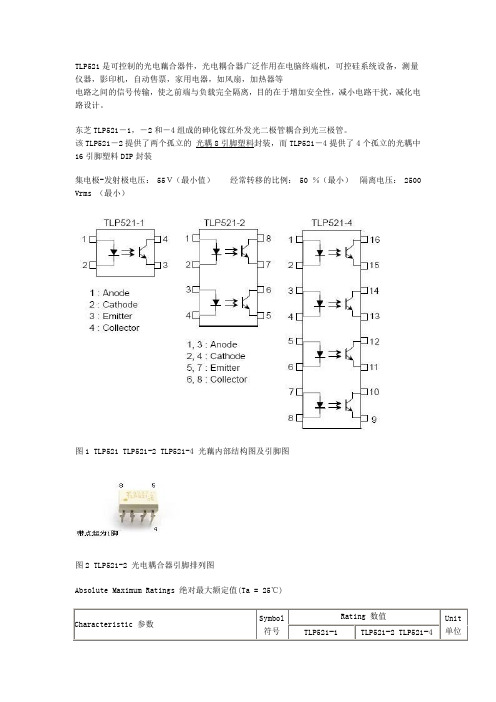
TLP521是可控制的光电藕合器件,光电耦合器广泛作用在电脑终端机,可控硅系统设备,测量仪器,影印机,自动售票,家用电器,如风扇,加热器等电路之间的信号传输,使之前端与负载完全隔离,目的在于增加安全性,减小电路干扰,减化电路设计。
东芝TLP521-1,-2和-4组成的砷化镓红外发光二极管耦合到光三极管。
该TLP521-2提供了两个孤立的光耦8引脚塑料封装,而TLP521-4提供了4个孤立的光耦中16引脚塑料DIP封装集电极-发射极电压: 55V(最小值)经常转移的比例: 50 %(最小)隔离电压: 2500 Vrms (最小)图1 TLP521 TLP521-2 TLP521-4 光藕内部结构图及引脚图图2 TLP521-2 光电耦合器引脚排列图Absolute Maximum Ratings 绝对最大额定值(Ta = 25℃)注:使用连续负载很重的情况下(如高温/电流/温度/电压和重大变化等),可能会导致本产品的可靠性下降明显甚至损坏。
Recommended Operating Conditions建议操作条件*1: Ex. rank GB: TLP521−1 (GB)(Note): Application type name for certification test, please use standard product type name, i.e.TLP521−1 (GB): TLP521−1, TLP521−2 (GB): TLP521−2Individual Electrical Characteristic 单独的电气特性参数(Ta = 25℃)Coupled Electrical Characteristic 耦合电气特性参数s(Ta = 25℃)Isolation Characteristic 耦合电气特性参数(Ta = 25℃)Switching Characteristic 开关特性参数(Ta = 25℃)图3 TLP521-1 封装图图4 TLP521-2 封装图图5 TLP521-4 封装图图6 开关时间测试电路特性曲线图:应用电路:图7 打开或关闭12V直流电动机的TTL控制信号输入电路图74HC04 特性:∙缓冲输入∙传输延迟(典型值): 6ns at V CC = 5V, C L = 15pF, T A= 25°C∙扇出(驱动)能力: (在温度范围内)- 标准输出 . . . . . . . . . . . . . . . 10 LSTTL Loads- 总线驱动 . . . . . . . . . . . . . . . 15 LSTTL Loads ∙宽工作温度范围 . . . –55°C to 125°C∙对称的传输延迟和转换时间∙相对于LSTTL逻辑IC,功耗减少很多∙HC Types- 工作电压:2V到6V- 高抗扰度: N IL = 30%, N IH= 30% of V CC at V CC = 5V∙HCT Types- 工作电压:4.5V到5.5V- 兼容直接输入LSTTL逻辑信号, V IL= 0.8V (Max), V IH = 2V (Min)- 兼容CMOS逻辑输入, I l1μA at V OL, V O该74HC04/74HCT04是高速CMOS器件,低功耗肖特基的TTL(LSTTL)电路。
- 1、下载文档前请自行甄别文档内容的完整性,平台不提供额外的编辑、内容补充、找答案等附加服务。
- 2、"仅部分预览"的文档,不可在线预览部分如存在完整性等问题,可反馈申请退款(可完整预览的文档不适用该条件!)。
- 3、如文档侵犯您的权益,请联系客服反馈,我们会尽快为您处理(人工客服工作时间:9:00-18:30)。
LV5217GPOverviewThis LV5217GP is 3-channel LED driver for cell phones. Each LED driver current can be adjusted by I2C bus. LV5217GP can perform various illumination effects with a full-color LED display.Features• Three color LED driver circuits.• The LED current can be switched independently in 7-bit units (0.31 to 25.48mA).• Independent on/off control of the three LED drivers (independent control of the 3 RGB colors). • Each LED drive current level can be adjusted independently over the I 2C bus. • Miniature package.• Thermal shutdown circuit.SpecificationsAbsolute Maximum Ratings at Ta = 25°CParameter SymbolConditionsRatingsUnitSupply voltage 1 V CC max 6.0V Supply voltage 2 V DD max 6.0V Maximum input current V IN B 6.0V Maximum output current I O max 30.0mA STBY pin voltageV STBY6.0V Allowable power dissipation Pd max Mounted on the specified board * 0.55W Operating temperature Topr -30 to +75°C Storage temperatureTstg-40 to +125°CThe specified board * : 50mm × 40mm × 0.8mm glass epoxy (4-layer circuit board).Bi-CMOS IC3ch LED DriverRecommended Operating Conditions at Ta = 25°CParameter SymbolConditionsRatingsUnit Supply voltage 1 V CC 3.0 to 4.5 V Supply voltage 2V DD1.6 to 3.0VElectrical Characteristics Ta = 25°C, V CC = 3.7V, V DD = 1.8V, RT = 56k Ω, Unless otherwise specified.RatingsParameter SymbolConditionsmin typ maxUnitOverall Characteristics Current drain 1 I CC 1 STBY = L *15μACurrent drain 2I CC 2 STBY = H, LED ON= L *1With the default serial data settings 0.7 2 mAHigh-level input voltage 1 V IN H1 Serial data signals, LEDON pin V DD ×0.8V Low-level input voltage 1 V IN L1Serial data signals, LEDON pinV DD ×0.2 VHigh-level input voltage 2 V IN H2 STBY pin 1.4V Low-level input voltage 2 V IN L2 STBY pin0.2 VLED Driver Block Minimum output current I MIN When the serial data is 0000001, V O = 0.5V 0.00.2 1.0 mA Maximum output current I MAX When the serial data is 1111111, V O = 0.5V 23.025.428.0 mA LED current value accuracyIDIF When current value is set to 4mA (0010011)-8 8 % Differential linearity error DLE *2-22 LSB LED pin saturation voltage VLED At the maximum current setting 0.3 V Leakage current ILEAKDrivers : off, V O = 5V1μAV O : LED pin voltage.*1. The sum of the V CC and V DD current drain values.*2. Differential linearity error : The difference between the actual and ideal amounts when one low-order bit value is added.Package Dimensionsunit : mm (typ) 3318Ambient temperature, Ta –°CA l l o w a b l e p o w e r d i s s i p a t i o n , P d m a x –WBlock DiagramNote 1 : The TEST pin must be tied to ground.Pin FunctionsPin No. Pin name Function1TESTTest signal input: This pin must be connected to ground.2 GND Ground3 RT Reference current setting resistor connection 4LEDONExternal LED control pin5 NC5 No connection6 NC6 No connection7 V CC Circuit system power supply8 SDAI Serial data signal input 9SCLISerial clock signal input10 NC10 Noconnection 11 NC11 No connection 12 V DD Power supply for logic system13 STBY Standby mode control14 RLED Red LED driver output 15 GLED Green LED driver output 16BLEDBlue LED driver outputSDAIV CCNC6NC5V NC11NC10SCL1Continued on next page.Power Supply Application1. Either bring up V CC and V DD at the same time, or bring up V CC first then V DD.2. Then, set the serial data. (After the serial data has been set, a period of about 2μs is required as the startup time forthe IC internal circuits.)3. Finally, clear the STBY pin states.Serial Data MapRegister address DataA7 A6 A5 A4 A3 A2 A1 A0 D7 D6 D5 D4 D3 D2 D1 D0RSW R[6:0]0 0 0 0 0 0 0 00 0 0 0 0 0 0 0GSW G[6:0]0 0 0 0 0 0 0 10 0 0 0 0 0 0 0BSW B[6:0]0 0 0 0 0 0 1 00 0 0 0 0 0 0 0 Upper row : Register name, Lower row : default valueSerial Data Mode SettingsR mode0 0 0 0 0 0 0 0 D7 D6 D5 D4 D3 D2 D1 D0LEDR output settingD7 RSW(default)0 OFF1 ONG mode0 0 0 0 0 0 0 1 D7 D6 D5 D4 D3 D2 D1 D0LEDR output settingD7 GSW0 OFF(default)1 ONB mode0 0 0 0 0 0 1 0 D7 D6 D5 D4 D3 D2 D1 D0LEDR output settingD7 BSW(default)0 OFF1 OND6-D0 current setting (Common to R, G and B)[mA] D6 D5 D4 D3 D2 D1 D0 Current*10 0 0 0 0 0 0 0.1(Default)0 0 0 0 0 0 1 0.310 0 0 0 0 1 0 0.520 0 0 0 0 1 1 0.720 0 0 0 1 0 0 0.930 0 0 0 1 0 1 1.130 0 0 0 1 1 0 1.340 0 0 0 1 1 1 1.540 0 0 1 0 0 0 1.740 0 0 1 0 0 1 1.940 0 0 1 0 1 0 2.140 0 0 1 0 1 1 2.340 0 0 1 1 0 0 2.540 0 0 1 1 0 1 2.740 0 0 1 1 1 0 2.950 0 0 1 1 1 1 3.150 0 1 0 0 0 0 3.350 0 1 0 0 0 1 3.460 0 1 0 0 1 0 3.760 0 1 0 0 1 1 3.970 0 1 0 1 0 0 4.170 0 1 0 1 0 1 4.370 0 1 0 1 1 0 4.570 0 1 0 1 1 1 4.760 0 1 1 0 0 0 4.970 0 1 1 0 0 1 5.170 0 1 1 0 1 0 5.370 0 1 1 0 1 1 5.570 0 1 1 1 0 0 5.780 0 1 1 1 0 1 5.980 0 1 1 1 1 0 6.180 0 1 1 1 1 1 6.390 1 0 0 0 0 0 6.600 1 0 0 0 0 1 6.800 1 0 0 0 1 0 6.990 1 0 0 0 1 1 7.190 1 0 0 1 0 0 7.390 1 0 0 1 0 1 7.600 1 0 0 1 1 0 7.800 1 0 0 1 1 1 7.990 1 0 1 0 0 0 8.190 1 0 1 0 0 1 8.400 1 0 1 0 1 0 8.600 1 0 1 0 1 1 8.800 1 0 1 1 0 0 9.000 1 0 1 1 0 1 9.200 1 0 1 1 1 0 9.400 1 0 1 1 1 1 9.600 1 1 0 0 0 0 9.800 1 1 0 0 0 1 10.000 1 1 0 0 1 0 10.200 1 1 0 0 1 1 10.400 1 1 0 1 0 0 10.600 1 1 0 1 1 1 11.20 0 1 1 1 0 0 0 11.40 0 1 1 1 0 0 1 11.60 0 1 1 1 0 1 0 11.80 0 1 1 1 0 1 1 12.00 0 1 1 1 1 0 0 12.20 0 1 1 1 1 0 1 12.40 0 1 1 1 1 1 0 12.600 1 1 1 1 1 1 12.801 0 0 0 0 0 0 12.99 1 0 0 0 0 0 1 13.19 1 0 0 0 0 1 0 13.39 1 0 0 0 0 1 1 13.59 1 0 0 0 1 0 0 13.79 1 0 0 0 1 0 1 13.98 1 0 0 0 1 1 0 14.18 1 0 0 0 1 1 1 14.38 1 0 0 1 0 0 0 14.58 1 0 0 1 0 0 1 14.78 1 0 0 1 0 1 0 14.97 1 0 0 1 0 1 1 15.17 1 0 0 1 1 0 0 15.37 1 0 0 1 1 0 1 15.57 1 0 0 1 1 1 0 15.77 1 0 0 1 1 1 1 15.96 1 0 1 0 0 0 0 16.16 1 0 1 0 0 0 1 16.36 1 0 1 0 0 1 0 16.56 1 0 1 0 0 1 1 16.76 1 0 1 0 1 0 0 16.96 1 0 1 0 1 0 1 17.15 1 0 1 0 1 1 0 17.35 1 0 1 0 1 1 1 17.55 1 0 1 1 0 0 0 17.75 1 0 1 1 0 0 1 17.95 1 0 1 1 0 1 0 18.15 1 0 1 1 0 1 1 18.34 1 0 1 1 1 0 0 18.54 1 0 1 1 1 0 1 18.74 1 0 1 1 1 1 0 18.94 1 0 1 1 1 1 1 19.14 1 1 0 0 0 0 0 19.33 1 1 0 0 0 0 1 19.53 1 1 0 0 0 1 0 19.73 1 1 0 0 0 1 1 19.93 1 1 0 0 1 0 0 20.13 1 1 0 0 1 0 1 20.32 1 1 0 0 1 1 0 20.52 1 1 0 0 1 1 1 20.72 1 1 0 1 0 0 0 20.92 1 1 0 1 0 0 1 21.12 1 1 0 1 0 1 0 21.31 1 1 0 1 0 1 1 21.511 1 0 1 1 1 0 22.111 1 0 1 1 1 1 22.301 1 1 0 0 0 0 22.501 1 1 0 0 0 1 22.701 1 1 0 0 1 0 22.901 1 1 0 0 1 1 23.101 1 1 0 1 0 0 23.291 1 1 0 1 0 1 23.491 1 1 0 1 1 0 23.691 1 1 0 1 1 1 23.891 1 1 1 0 0 0 24.091 1 1 1 0 0 1 24.291 1 1 1 0 1 0 24.481 1 1 1 0 1 1 24.681 1 1 1 1 0 0 24.881 1 1 1 1 0 1 25.081 1 1 1 1 1 0 25.281 1 1 1 1 1 1 25.48 * Note 1 : There is significant current variance, so care should be taken for use. The current value can be set when D7 is “0.”Serial Bus Communication Specifications I 2C serial transfer timing conditionsStandard modeParameter symbolConditions min typ max unitSCL clock frequency fscl SCL clock frequency0 100kHz ts1 The SCL setup time from the SDA rising edge 4.7 μs ts2 The SDA setup time from the SCL rising edge 250 ns Data setup timets3The SCL setup time from the SDA rising edge 4.0 μs th1 The SCL hold time from the SDA falling edge 4.0 μs Data hold timeth2The SDA hold time from the SCL falling edge 0 μs twL SCL low period pulse width 4.7 μs Pulse widthtwHSCL high period pulse width 4.0μs ton SCL, SDA (input) rising time 1000ns Input waveform conditionstofSCL, SDA (input) falling time300ns Bus free timetbufTime between STOP and TART conditions4.7μsHigh-speed modeParameter SymbolConditionsmin typ max unitSCL clock frequency fscl SCL clock frequency0 400kHz ts1 The SCL setup time from the SDA rising edge 0.6 μs ts2 The SDA setup time from the SCL rising edge 100ns Data setup timets3The SCL setup time from the SDA rising edge 0.6 μs th1 The SCL hold time from the SDA falling edge 0.6 μs Data hold timeth2The SDA hold time from the SCL falling edge 0 μs twL SCL low period pulse width 1.3 μs Pulse widthtwHSCL high period pulse width 0.6μs ton SCL, SDA (input) rising time 300ns Input waveform conditionstofSCL, SDA (input) falling time300ns Bus free timetbufTime between STOP condition and TART condition1.3μs分销商库存信息: ONSEMILV5217GP-TE-L-E。