MN1526_SSE-25640-1
AN_SY8088_CONTEC_Vinson
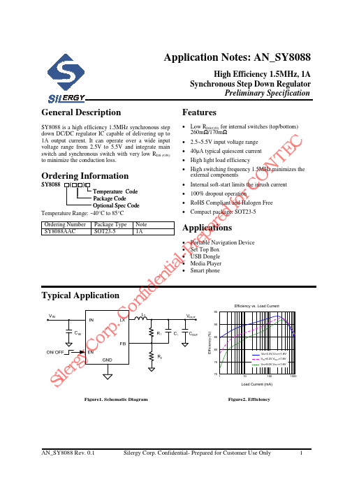
Application Notes: AN_SY8088High Efficiency 1.5MHz, 1A Synchronous Step Down Regulator Preliminary SpecificationGeneral DescriptionSY8088 is a high efficiency 1.5MHz synchronous step down DC/DC regulator IC capable of delivering up to 1A output current. It can operate over a wide input voltage range from 2.5V to 5.5V and integrate main switch and synchronous switch with very low RDS (ON) to minimize the conduction loss.Features• Low RDS(ON) for internal switches (top/bottom) 260mΩ/170mΩ • 40µA typical quiescent current • High light load efficiency • 2.5~5.5V input voltage range.C onTypical Applicationfidentia l-P re pOrdering Number SY8088AACPackage Type SOT23-5Note 1AApplications• • • • •Portable Navigation Device Set Top Box USB Dongle Media Player Smart phonear edTemperature Code Package Code Optional Spec Code Temperature Range: -40°C to 85°C• 100% dropout operation• Compact package: SOT23-59590Co rp8580 VIN=3.3V,VOUT=1.8V VIN=4.2V,VOUT=1.8V 75 VIN=5.0V,VOUT=1.8Ver gy70fo• RoHS Compliant and Halogen FreerC10SY8088 □(□□)□• Internal soft-start limits the inrush currentEfficiency vs. Load CurrentOOrdering Information• High switching frequency 1.5MHz minimizes the external componentsSil1Load Current (mA)Figure1. Schematic DiagramFigure2. EfficiencyAN_SY8088 Rev. 0.1Silergy Corp. Confidential- Prepared for Customer Use OnlyN TE100C10001AN_SY8088Pinout (Top View)(SOT23-5)Top Mark: LDxyz (device code: LD, x=year code, y=week code, z= lot number code) Pin Name EN GND LX IN FB Pin Number 1 2 3 4 5Absolute Maximum Ratings (Note 1)Recommended Operating Conditions (Note 3)AN_SY8088 Rev. 0.1Siler gySupply Input Voltage ----------------------------------------------------------------------------------------------- 2.5V to 5.5V Junction Temperature Range ----------------------------------------------------------------------------------- -40°C to 125°C Ambient Temperature Range ------------------------------------------------------------------------------------ -40°C to 85°CCo rpSupply Input Voltage -------------------------------------------------------------------------------------------------------- 6.0V Enable, FB Voltage---------------------------------------------------------------------------------------------------- VIN + 0.6V Power Dissipation, PD @ TA = 25°C, SOT23-5--------------------------------------------------------------------------- 0.6W Package Thermal Resistance (Note 2) θ JA -------------------------------------------------------------------------------------------------------------- 170°C/W θ JC ---------------------------------------------------------------------------------------------------------- ----130°C/W Junction Temperature Range ----------------------------------------------------------------------------------------------125°C Lead Temperature (Soldering, 10 sec.) ---------------------------------------------------------------------------------- 260°C Storage Temperature Range ----------------------------------------------------------------------------------- -65°C to 150°C.C onSilergy Corp. Confidential- Prepared for Customer Use Onlyfidentia l-P re pPin Description Enable control. Pull high to turn on. Do not float. Ground pin. Inductor pin. Connect this pin to the switching node of the inductor. Input pin. Decouple this pin to the GND pin with at least 4.7uF ceramic capacitor. Output Feedback Pin. Connect this pin to the center point of the output resistor divider (as shown in Figure 1) to program the output voltage: VOUT=0.6*(1+R1/R2).Add optional C1 (10pF~47pF) to speed up the transient response.ar edforCON TE2CAN_SY8088Electrical Characteristics(VIN = 5V, VOUT = 2.5V, L = 2.2uH, COUT = 10uF, TA = 25°C, unless otherwise specified)Note 3: The device is not guaranteed to function outside its operating conditions.AN_SY8088 Rev. 0.1Siler gyCo rp.C onNote 2: θ JA is measured in the natural convection at TA = 25°C on a low effective single layer thermal conductivity test board of JEDEC 51-3 thermal measurement standard. Exposed Paddle of DFN package is the case position for θ JC measurement.Silergy Corp. Confidential- Prepared for Customer Use OnlyfidenNote 1: Stresses beyond the “Absolute Maximum Ratings” may cause permanent damage to the device. These are for stress ratings. Functional operation of the device at these or any other conditions beyond those indicated in the operational sections of the specifications is not implied. Exposure to absolute maximum rating conditions for extended periods may remain possibility to affect device reliability.tia l-P re pNFET RON PFET Current Limit EN rising threshold EN falling threshold Input UVLO threshold UVLO hysteresis Oscillator Frequency Min ON Time Max Duty Cycle Soft Start Time Thermal Shutdown Temperature Thermal Shutdown Hysteresisar edTSS TSD THYSfoRDS(ON),N ILIM VENH VENL VUVLO VHYS FOSCN TE170Parameter Input Voltage Range Quiescent Current Shutdown Current Feedback Reference Voltage PFET RONSymbol VIN IQ ISHDN VREF RDS(ON),PTest Conditions IOUT=0, VFB=VREF ⋅ 105% EN=0Min 2.5Typ 40 0.1 0.6 260Max 5.5 1 0.612O0.1 1.5 80 1 160 151.3 1.5rC1000.4 2.5C0.588Unit V µA µA V mΩmΩ A V V V V MHz ns % ms °C °C3AN_SY8088Typical Performance CharacteristicsEfficiency vs. Load Current95 95Efficiency vs. Load Current90908580 75 VIN=3.3V,VOUT=1.2V VIN=4.2V,VOUT=1.2V 70 VIN=5.0V,VOUT=1.2V 7565110100100070rC10 ∆Vout LX ILO1N TEVIN=4.2V,VOUT=1.8V VIN=5.0V,VOUT=1.8V 10080VIN=3.3V,VOUT=1.8V100ar edEfficiency vs. Load Current9590tia l-P re p85 VIN=4.2V,VOUT=3.3V VIN=5V,VOUT=3.3V 7580en70110100fid1000Load Current (mA) Output Ripple.C onfoLoad Current (mA)Load Current (mA) Output Ripple(VIN=5.0V, VOUT=1.8V, ILOAD=0A)20mV/div2.0V/div0.5A/divTime (400ns/div) Output Ripple(VIN=5.0V, VOUT=1.8V, ILOAD=1A) ∆Vout 20mV/div(VIN=5.0V, VOUT=1.8V, ILOAD=0.2A) ∆VoutLXCo rp20mV/div2.0V/divLX2.0V/diver gyIL1.0A/divSilIL0.5A/divTime (400ns/div)Time (400ns/div)AN_SY8088 Rev. 0.1Silergy Corp. Confidential- Prepared for Customer Use OnlyC1000854AN_SY8088Startup from Enable(VIN=5.0V, VOUT=1.8V, ILOAD=1.0A)Shutdown from Enable(VIN=5.0V, VOUT=1.8V, ILOAD=1.0A)EN5.0V/divEN5.0V/divVOUT1.0V/divVOUT1.0V/divLX5.0V/divIL1.0A/divAN_SY8088 Rev. 0.1Siler gyCo rp.C onSilergy Corp. Confidential- Prepared for Customer Use Onlyfidentia l-P re par edforCTime (400µs/div)Time (40µs/div)ON TEILC1.0A/divLX5.0V/div5AN_SY8088OperationThe SY8088 is a high-efficiency 1.5MHz synchronous step-down DC-DC converters capable of delivering up to 1A output current. It operates over a wide input voltage range from 2.5V to 5.5V and integrates main switch and synchronous switch with very low RDS(ON) to minimize the conduction loss. where Fsw is the switching frequency and Iout,max is the maximum load current. The SY8088 regulator IC is quite tolerant of different ripple current amplitude. Consequently, the final choice of inductance can be slightly off the calculation value without significantly impacting the performance. 2) The saturation current rating of the inductor must be selected to be greater than the peak inductor current under full load conditions. VOUT(1-VOUT/VIN,MAX) ISAT, MIN > IOUT, MAX + 2 ⋅ FSW ⋅ L 3) The DCR of the inductor and the core loss at the switching frequency must be low enough to achieve the desired efficiency requirement. It is desirable to choose an inductor with DCR<50mohm to achieve a good overall efficiency. Short Circuit Protection: After soft start is over, output voltage is below 40% of the regulation level, IC the internal softstart node is discharged and the error amplifier output is reset to minimum. Then the part will restart after 2ms. The frequency is folded back to about 30% of the nominal frequency and the current limit is folded back to 1.0A to prevent the inductor current from runaway and to reduce the power dissipation of the IC under short circuit conditions. Load Transient Considerations: The SY8088 regulator IC integrates the compensation components to achieve good stability and fast transient responses. In some applications, adding a 22pF ceramic cap in parallel with R1 may further speed up the load transient responses and is thus recommended for applications with large load transient step requirements. Layout Design: The layout design of SY8088 regulator is relatively simple. For the best efficiency and minimum noise problems, we should place the following components close to the IC: CIN, L, R1 and R2. 1) It is desirable to maximize the PCB copper area connecting to GND pin to achieve the best thermal and noise performance. If the board space allowed, a ground plane is highly desirable. 2) CIN must be close to Pins IN and GND. The loop area formed by CIN and GND must be minimized. 3) The PCB copper area associated with LX pin must be minimized to avoid the potential noise problem.R1 =(VOUT − 0.6 V) ⋅ R2 0.6VOutput inductor L: There are several considerations in choosing this inductor. 1) Choose the inductance to provide the desired ripple current. It is suggested to choose the ripple current to be about 40% of the maximum output current. The inductance is calculated as: VOUT (1 − VOUT/VIN,MAX ) L= FSW × IOUT,MAX × 40%AN_SY8088 Rev. 0.1Siler gyOutput capacitor COUT: The output capacitor is selected to handle the output ripple noise requirements. Both steady state ripple and transient requirements must be taken into consideration when selecting this capacitor. For the best performance, it is recommended to use X7R or better grade ceramic capacitor with 6V rating and greater than 4.7uF capacitance.Co rp.C onInput capacitor CIN: A typical X7R or better grade ceramic capacitor with 6V rating and greater than 4.7uF capacitance is recommended. To minimize the potential noise problem, place this ceramic capacitor really close to the IN and GND pins. Care should be taken to minimize the loop area formed by CIN, and IN/GND pins.Silergy Corp. Confidential- Prepared for Customer Use Onlyfidentia l-P re pFeedback resistor dividers R1 and R2: Choose R1 and R2 to program the proper output voltage. To minimize the power consumption under light loads, it is desirable to choose large resistance values for both R1 and R2. A value of between 100kΩ and 1MΩ is highly recommended for both resistors. If R2=120kΩ is chosen, then R1 can be calculated to be:ar edforCBecause of the high integration in the SY8088 IC, the application circuit based on this regulator IC is rather simple. Only input capacitor CIN, output capacitor COUT, output inductor L and feedback resistors (R1 and R2) need to be selected for the targeted applications specifications.ON TEApplications InformationC6AN_SY80884) The components R1 and R2, and the trace connecting to the FB pin must NOT be adjacent to the LX net on the PCB layout to avoid the noise problem. 5) If the system chip interfacing with the EN pin has a high impedance state at shutdown mode and the IN pin is connected directly to a power source such as a LiIon battery, it is desirable to add a pull down 1Mohm resistor between the EN and GND pins to prevent the noise from falsely turning on the regulator at shutdown mode.AN_SY8088 Rev. 0.1Siler gyCo rp.C onSilergy Corp. Confidential- Prepared for Customer Use Onlyfidentia l-P re par edforC7ON TECAN_SY8088SOT23-5 Package outline & PCB layout design0.552.80 - 3.102.70 - 3.00Recommended Pad Layouttia l-P re par ed0.95 TYPfo0.30 - 0.50rC0.25 REF1.0 - 1.30.80O0.95 TYP 1.90 TYP 0.01 - 0.10.1 - 0.15AN_SY8088 Rev. 0.1Siler gyCo rpNotes: All dimensions are in millimeters. All dimensions don’t include mold flash & metal burr..C onSilergy Corp. Confidential- Prepared for Customer Use Onlyfid0.3 - 0.6enN TE1.50 - 1.702.40C8。
eKTH3900_Product Spec_draft_1221
Trademark Acknowledgments:IBM is a registered trademark and PS/2 is a trademark of IBM.Windows is a trademark of Microsoft Corporation.ELAN and ELAN logo are trademarks of ELAN Microelectronics Corporation.Copyright © 2010 by ELAN Microelectronics CorporationAll Rights ReservedELAN Korea Electronics Co., LtdRm No. 1101, Incheon Business Center, 636, Kojan-dong, Namdong-gu INCHEON, KOREA Tel : 82-32-814-7730Fax : 82-32-813-7730Shenzhen, Ltd.3F, SSMEC Bldg., Gaoxin S. Ave. IShenzhen Hi-tech Industrial Park(South Area), ShenzhenCHINA 518057Tel: +86 755 2601-0565Fax: +86 755 2601-0500elan-sz@Shanghai, Ltd.#34, First Fl., 2nd Bldg.,Lane 122, Chunxiao Rd.Zhangjiang Hi-Tech ParkShanghai, CHINA 201203Tel: +86 21 5080-3866Fax: +86 21 5080-4600elan-sh@eKTH3900Capacitive Touchpad Controller 1 Contents1CONTENTS (1)2GENERAL DESCRIPTION (1)3FEATURES (2)4BLOCK DIAGRAM (3)5466 6.16.26.379 810 911 9.11013 1114 11.111.2eKTH3900Capacitive Touchpad ControllerSpecification Revision History0.0 Draft 2012/12/21eKTH3900Capacitive Touchpad Controller2 General DescriptionThe eKTH3900 is a single-chip capacitive touch panel controller with high resolution ADC and powerful DSP. With mighty computing power, the controller can take care of lots of touch panel algorithm, even the multi-finger identification or gesture reorganization. It adopts mutual capacitance approaches which support true multi-touch capability. It provides high voltage (up to 12V) driving signals for a touch sensor. With the high voltage, it provides excellent noise immunity.eKTH3900Capacitive Touchpad Controller3 Features• Mutual Capacitive Sensing Techniques• Up to 10-finger detection and simultaneous tracking• Up to 100 Hz report rate• Sensor size up to 12 inch diagonal supported at 5mm electrode pitch (EKTH3912AY)eKTH3900Capacitive Touchpad Controller4 Block DiagramAs shown in the block diagram below and as per our general description, the eKTH3900 uses a modified Harvard architecture in such a way that the memory is organized into two separate fields, namely, Program ROM and Data RAM. As the memories are separate, the central processing unit can read/write data at the same time.eKTH3900Capacitive Touchpad Controller 5 Pin DescriptioneKTH3900Capacitive Touchpad ControllerTX[44:01] AO Touch panel driving traces. (EKTH3915SU)RX[35:01] RX[74:40] AI Touch panel sensing traces. (EKTH3915SU)TX[44:01] AO Touch panel driving traces. (EKTH3918SU)RX[78:01] AI Touch panel sensing traces. (EKTH3918SU)Rsvd N/A ReservedeKTH3900Capacitive Touchpad Controller6 Pinout6.1 EKTH3912AY BGA132 Pinout6.2 EKTH3915SU BGA168 Pinout8 •Product Specification (DRAFT) 12.21.20126.3EKTH3918SU BGA168 Pinout7 Absolute Maximum Ratings10 •Product Specification (DRAFT) 12.21.20128 Electrical CharacteristicsDC Electrical CharacteristicsVCCIO: 1.8V~3.6V ;VCC33: 3.0V~3.6V9 Power-on Sequence12 •Product Specification (DRAFT) 12.21.20129.1 Power Off and then Power On SequenceVCC3310 Application Circuits14 •Product Specification (DRAFT) 12.21.201211 Package Outlines11.1 B GA132 Package Outline (5x10x0.8mm)16 •Product Specification (DRAFT) 12.21.201211.2BGA168 Package Outline (5x13x0.8mm)eKTH3900 Capacitive Touchpad ControllerProduct Specification (DRAFT) 12.21.2012• 17(This specification is subject to change without further notice)。
搜博 SM1600B-160 温度采集模块工具软件 说明书
SM1600B-160搜博MODBUS温度采集模块工具软件说明书一、硬件需求 (3)二、软件需求 (3)三、软件安装步骤 (3)四、软件操作 (6)4.1主界面分布说明 (6)4.2 SM1600B-160与电脑连接 (6)4.3导入和导出序列号操作 (10)4.3.1 导出序列号 (10)4.3.2 导入序列号 (11)4.4 地址、功能码、起始地址、数据长度 (12)五、软件适用范围 (13)一、硬件需求硬盘空间大于1G,内存大于256M,CPU 单核及以上。
二、软件需求本软件仅限于windows XP,windows2000,windows2003环境使用,window 7请使用兼容windows xp模式。
三、软件安装步骤软件安程过程以下面描述为例,实际文字或软件内容部分根据软件版本有所不同。
图1软件安装图标找到“SM1600B-160 温度采集模块工具软件V14.11.13”文件名,双击并按以下说明进行安装操作。
图2软件安装过程直接点下一步。
图3软件安装选择安装路径选择合适的安装路径,也可以直接选择默认路径,还可更改到其它目录进行安装。
图4软件安装过程显示选定的安装目标直接点击“安装”。
图5 安全卫士360木马防护墙提示若弹出以上木马提示,可以选择“允许本次操作”,本软件绝无木马,请放心安装,让360放行。
若多次提示,可以先关掉防火墙后再进行安装操作。
一直点击【下一步】即可完成安装。
成功安装后,点击桌面快捷键即可运行软件。
四、软件操作4.1主界面分布说明图6软件主界面分布4.2 SM1600B-160与电脑连接与电脑连接需要USB转RS485信号线一条以及相应的驱动程序。
程序正确安装并插入信号线后在我的电脑—属性—硬件—设备管理器—端口。
查看USB转RS485是用的哪一个端口,从图7中来看是COM3。
图7电脑的端口打开软件,进入到仪器设置界面。
如图8所示:图8需要修改串口设置以达到连接到硬件。
NUVOTON NM1817系列微控制器数据手册说明书
ARM Cortex™-M032-BIT MICROCONTROLLER NM1817 Series Product BriefNM1817 SERIES DATASHEET The information described in this document is the exclusive intellectual property ofNuvoton Technology Corporation and shall not be reproduced without permission from Nuvoton.Nuvoton is providing this document only for reference purposes of NuMicro TM microcontroller basedsystem design. Nuvoton assumes no responsibility for errors or omissions.All data and specifications are subject to change without notice.For additional information or questions, please contact: Nuvoton Technology Corporation.TABLE OF CONTENTS1GENERAL DESCRIPTION (3)2FEATURES (4)3PARTS INFORMATION LIST AND PIN CONFIGURATION (8)3.1Selection Guide (8)3.2Pin Configuration (8)3.2.1LQFP44-pin (8)3.3Pin Description (9)4BLOCK DIAGRAM (13)4.1NM1817 Block Diagram (13)5NM1817 ELECTRICAL CHARACTERISTICS (14)5.1NM1120 Absolute Maximum Ratings (14)5.2NM1120 DC Electrical Characteristics (15)5.3NM1120 AC Electrical Characteristics (20)5.3.1**External Input Clock (function has been reserved in NM1817) (20)5.3.2**External 4~24MHz High Speed Crystal (HXT)(function has been reserved in NM1817)215.3.3**Typical Crystal Application Circuits (function has been reserved in NM1817) (21)5.3.448MHz Internal High Speed RC Oscillator (HIRC) (21)5.3.510kHz Internal Low Speed RC Oscillator (LIRC) (21)5.4NM1120 Analog Characteristics (22)5.4.112-bit SAR ADC (22)5.4.2LDO & Power Management (23)5.4.3Brown-out Detector (23)5.4.4Power-on Reset (24)5.4.5Comparator (24)NM1817 SERIES DATASHEET5.4.6PGA (24)5.4.7Temperature Sensor (25)5.5NPT23011 Absolute Maximum Ratings (25)5.6NPT23011 Recommended Operating Conditions (26)5.7NPT23011 Static Electrical Characteristics (26)5.8NPT23011 Dynamic Electrical Characteristics (27)5.9DC Electrical Characteristic for LDO_5V_OUT (27)6PACKAGE DIMENSION (28)6.1LQFP 44-pin(10mm x 10mm) (28)7ORDERING INFORMATION (30)8REVISION HISTORY (31)1 GENERAL DESCRIPTIONThe NM1817 series 32-bit microcontroller(MCU) is embedded with ARM®Cortex™-M0 core andthree phase half-bridge power MOSFET and IGBT drivers with independent high and low sidereferenced output channels for motor driver applications which require high performance andintegration. The Cortex™-M0 is the ARM® embedded processor with 32-bit performance at a costequivalent to the traditional 8-bit microcontroller.The MCU of NM1817 series can run up to 48MHz and offers 29.5K-bytes embedded program flash,size configurable Data Flash (shared with program flash), 2K-byte flash for the ISP, 1.5K-byteSPROM for security, and 4K-byte SRAM. Plentiful system level peripheral functions, such as I/OPort, Timer, UART, SPI, I2C, PWM, ADC, Watchdog Timer, Analog Comparator and Brown-outDetector, have been incorporated into the NM1817 series in order to reduce component count,board space and system cost. These useful functions make the NM1817 series powerful for a widerange of motor driver applications.The floating channel can be used to drive an N-channel power MOSFET or IGBT in the high sideconfiguration which operates up to 600 volts. It’s also built-in the temperature sense output signalfor MCU detection & one comparator for over current protectionAdditionally, the NM1817 is equipped with ISP (In-System Programming) and ICP (In-CircuitProgramming) functions, which allow the user to update the program memory without removing thechip from the actual end product.NM1817 is the combination of NM1120 and NPT23011 Gate Driver. User may refer to the TRM ofNM1120 and the datasheet of NPT23011 for the detailed specification. The NM1120 BSP is alsofor NM1817 software developing.NM1120NPT23011NM1817NM1817 SERIES DATASHEETNM1817 SERIES DATASHEET2 FEATURES● Gate Driver⏹ Programmable enable/disable gate driver by MCU I/O of PC.4⏹ Floating channel designed for bootstrap operation up to + 600V⏹ Gate driver supply range from 12 to 18V⏹ VCC/VBS Under-voltage lock-out⏹ Cross conduction prevention⏹ High side output in phase with HIN● MCU Core⏹ ARM ® Cortex™-M0 core running up to 48MHz⏹ One 24-bit system timer⏹ Supports Low Power idle mode.⏹ A single-cycle 32-bit hardware multiplier⏹ NVIC for the 32 interrupt inputs, each with 4-level of priority⏹ Supports Serial Wire Debug (SWD) interface and two watch points/fourbreakpoints● Memory⏹ 29.5Kbytes Flash memory for program memory (APROM)⏹ Configurable Flash memory for data memory (Data Flash)⏹ 2KB Flash memory for loader (LDROM)⏹ Three 0.5KB Flash memory for security protection (SPROM)⏹ 4KB SRAM for internal scratch-pad RAM (SRAM)● Clock Control⏹ 48MHz internal oscillator (HIRC) (±1% accuracy at 250C, 5V)⏹ 10kHz internal low-power oscillator (LIRC) for Watchdog Timer and idle wake-up ● I/O Port⏹ Up to 15 general-purpose I/O (GPIO) pins⏹ Four I/O modes:◆ Quasi-bidirectional input/output◆ Push-Pull output◆ Open-Drain output◆ Input only with high impedance⏹ Optional TTL/Schmitt trigger input⏹ I/O pin can be configured as interrupt source with edge/level setting ⏹ Supports high driver and high sink I/O mode⏹ GPIO built-in Pull-up/Pull-low resistor for selection.● Timer⏹ Provides two channel 32-bit Timers; one 8-bit pre-scalar counter with 24-bit up-NM1817 SERIES DATASHEETtimer for each timer⏹ Independent clock source for each timer⏹ Provides One-shot, Periodic, Toggle and Continuous operation modes ⏹ 24-bit up counter value is readable through TDR (Timer Data Register) ⏹ Provides trigger counting/free counting/counter reset function triggered byexternal capture pin or internal comparator signal⏹ Supports event counter function⏹ Supports Toggle Output mode⏹ Supports wake-up from Idle or Power-down mode● Continuous Capture⏹ Timer0, Timer1 and Systick support Continuous Capture function which cancontinuously capture at most 4 edges on one signal● Enhanced Input Capture⏹ One unit of 24-bit input capture counter.⏹ Capture source:◆ I/O inputs: ECAP0, ECAP1 and ECAP2◆ ACMP Trigger◆ ADC Trigger● WDT (Watchdog Timer)⏹ Programmable clock source and time-out period⏹ Supports wake-up function in Power-down mode and Idle mode⏹ Interrupt or reset selectable on watchdog time-out● EPWM(Enhanced PWM Generator)⏹ Support a built-in 16-bit PWM clock generators, providing six PWM outputs orthree complementary paired PWM outputs⏹ Shared same clock source, clock divider, period and dead-zone generator ⏹ Supports group/independent/complementary modes⏹ Supports One-shot or Auto-reload mode⏹ Supports Edge-aligned and Center-aligned type⏹ Support Asymmetric mode⏹ Programmable dead-zone insertion between complementary channels ⏹ Each output has independent polarity setting control⏹ Hardware fault brake and software brake protections⏹ Supports rising, falling, central, period, and fault break interrupts⏹ Supports duty/period trigger A/D conversion⏹ Timer comparing matching event trigger PWM to do phase change⏹ Supports comparator event trigger PWM to force PWM output low for currentperiod⏹ Provides interrupt accumulation function⏹ Gate driver PWM output by MCU PWM controlif the ENGD pin of NM1817 is set to high level, then the output status ofNM1120 and gate driver is as the following table.MCU PWM Control Gate Driver PWM OutputPWM0/2/4 PWM1/3/5 UHO/VHO/WHO ULO/VLO/WLOH L ON OFFL H OFF ONL L OFF OFFH H OFF OFFOtherwise, if the ENGD pin of NM1817 is set to low level, then the output of gate driver is all off.●BPWM (Basic PWM Generator)⏹One 16-bit PWM generator which supports one 8-bit pre-scalar, one clock divider,two PWM timers (down counter) and one dead-zone generator⏹Two independent outputs or one complementary paired outputs.⏹PWM Interrupt request synchronized with PWM period⏹Edge-aligned type or Center-aligned type option●USCI (Universal Serial Control Interface Controller)⏹Two USCI devices⏹Supports to be configured as UART, SPI, I²C individually⏹Supports programmable baud-rate generator●ADC (Analog-to-Digital Converter)⏹12-bit ADC with 1M SPS⏹Supports 2 sample/holdNM1817 SERIES DATASHEET⏹Up to 8-ch single-end inputfrom I/O and one internal input from band-gap.⏹Conversion started either by software trigger, PWM trigger, ACMP trigger orexternal pin trigger⏹Supports temperature sensor for measureing chip temperature⏹Support Simultaneous and Sequential function to continuous conversion 4channels maximum.●Programmable Gain Amplifier (PGA)⏹Supports 8 level gain selects from 1, 2, 3, 5, 7, 9, 11 and 13.⏹Unity gain frequency up to 8MHz●Analog Comparator⏹Two analog comparators with programmable 16-level internal voltage reference⏹Build-in CRV (comparator reference voltage)⏹Supports Hysteresis function⏹Interrupt when compared results changed●Hardware Divider⏹Signed (two’s complement) integer calculation⏹32-bit dividend with 16-bit divisor calculation capacity⏹32-bit quotient and 32-bit remainder outputs (16-bit remainder with sign extendsto 32-bit)⏹Divided by zero warning flag⏹ 6 HCLK clocks taken for one cycle calculation⏹Waiting for calculation ready automatically when reading quotient and remainder●ISP (In-System Programming) and ICP (In-Circuit Programming)●BOD (Brown-out Detector)⏹8 programmable threshold levels:4.3V/4.0V/3.7V/3.0V/2.7V/2.4V/2.2V/2.0V⏹Supports Brown-out interrupt and reset option●96-bit unique ID●LVR (Low Voltage Reset)●Operating Temperature: -40℃~105℃●Packages:⏹44-pin LQFP (10x10mm)⏹Package is Halogen-free, RoHS-compliant and TSCA-compliant.NM1817 SERIES DATASHEETNM1817 SERIES DATASHEET3 PARTS INFORMATION LIST AND PIN CONFIGURATION3.1 Selection Guide P a r t N u m b e rF l a s h (K B ) S R A M (K B )I S PL o a d e r R O M(K B ) D a t a F l a s h I /O T im e r Connectivity I R C 48 M H z * B O D P W M An a l o g C o m p .P G A A D C (12-B it )Te m p er a t u r eS e n s orIC P /I S P I /A PPac k a geUSCI U A R T * I 2C S P I NM1817NT 29.5 4 2 √ 15 2 2 2 2 1 1 6 2 1 8x12bit 1 √ LQFP44Table 3.1-1 NM1817 Series Selection Guide3.2 Pin Configuration3.2.1 LQFP44-pin2401436587109114438373635342930272825262324121314151718192021162231323342433941NM1817LQFP 44-pin PB.1/ADC0_CH1/ACMP0_P1/ECAP_P1PB.2/ADC0_CH2/BPWM_CH1/ACMP0_P2/ECAP_P2PC.1/ADC0_CH4/STADC/ACMP0_P3/ACMP1_P1/SPI0_MOSI/SPI1_MISO /RESET PC.3/ACMP1_O/PGA_O/SPI0_CLK/SPI1_SS PD.1/ICE_CLK/ACMP1_P2/I2C0_SCL/SPI0_CLK/SPI1_SS/UART0_TXD PC.0/ADC0_CH3/BPWM_CH0/ACMP1_P0/I2C1_SCL/SPI0_SS/SPI1_CLK/UART1_TXDNCPD.5/UART0_TXDU_VS NC V_LOW_LOU_LO W_HOPC.2/ADC1_CH2/BRAKE/CCAP_P1/I2C1_SDA/SPI0_MISO/SPI1_MOSI/UART1_RXD W_VB NCNCCOMVCCNC PB.3/ACMP1_N/PGA_I/TM0U_VB PD.6/UART0_RXD VDD PB.0/ADC0_CH0/ACMP0_P0/ECAP_P0VSS ENGD V_HO NC V_VS NC NCLDO_CAP NC PB.4/ADC1_CH0/ACMP0_N/TM1U_HO PD.4/BPWM_CH0/UART1_RXD V_VB W_VSLDO_5V_OUT PD.2/ICE_DAT/ADC1_CH1/CCAP_P0/I2C0_SDA/SPI0_MOSI/SPI1_MISO/UART0_RXD PD.3/BPWM_CH1/UART1_TXDFigure 3.2-1 NM1817 LQFP 44-pin Diagram3.3 Pin DescriptionNM1120 NPT23011 NM1817NTPin Name Pin Type Description TSSOP28 SOP-20 LQFP 44-pin2 LDO_5V_OUT A 5V LDO output26 4 ENGD I Gate driver enable pin. The pin is also internally connected to PC.4 of NM1120.27 5 LDO_CAP P LDO output pin28 6 VSS P Ground pin for digital circuit 1 7 VDD P Power supply for digital circuit2 8 PD.6 I/O General purpose digital I/O pin UART0_RXD I Data receiver input pin for UART0.3 9 PB.0 I/O General purpose digital I/O pin.ADC0_CH0 A ADC0 channel0 analog input.ACMP0_P0 A Analog comparator0 positive input pin. ECAP_P0 I Enhanced Input Capture input pin4 10 PB.1 I/O General purpose digital I/O pin.ADC0_CH1 A ADC0 channel1 analog input.ACMP0_P1 A Analog comparator0 positive input pin. ECAP_P1 I Enhanced Input Capture input pin5 11 PB.2 I/O General purpose digital I/O pin.ADC0_CH2 A ADC0 channel2 analog input.BPWM_CH1 I/O PWM channel1 output/capture input. ACMP0_P2 A Analog comparator0 positive input pin. ECAP_P2 I Input capture channel 26 12 PB.4 I/O General purpose digital I/O pin.ADC1_CH0 A ADC1 channel0 analog input.ACMP0_N A Analog comparator0 negative input pin. TM1 I/OTimer1 event counter input / toggleoutput7 13 PC.1 I/O General purpose digital I/O pin.ADC0_CH4 A ADC0 channel4 analog input.STADC I ADC external trigger input.ACMP0_P3 A Analog comparator0 positive input pin.ACMP1_P1 A Analog comparator1 positive input pin.SPI0_MOSI I/O SPI0 1st MOSI (Master Out, Slave In)pin.SPI1_MISO I/O SPI1 MISO (Master In, Slave Out) pin.NM1817 SERIES DATASHEET8 14 nRESET I External reset input: active LOW, withan internal pull-up. Set this pin low resetto initial state.9 15 PB.3 I/O General purpose digital I/O pin. ACMP1_N A Analog comparator1 negative input pin. PGA_I A PGA input pinTM0 I/O Timer0 event counter input / toggleoutput10 16 PC.2 I/O General purpose digital I/O pin.ADC1_CH2 A ADC1 channel2 analog input.BRAKE I Brake input pin of EPWM.CCAP_P1 I Timer Continuous Capture input pinI2C1_SDA I/O I2C1 data input/output pin.SPI0_MISO I/O SPI0 1st MISO (Master In, Slave Out)pin.SPI1_MOSI I/O SPI1 MOSI (Master Out, Slave In) pin. UART1_RXD I Data receiver input pin for UART1.11 17 PD.2 I/O General purpose digital I/O pin.ICE_DAT I/O Serial wired debugger data pinADC1_CH1 A ADC1 channel1 analog input.CCAP_P0 I Timer Continuous Capture input pinI2C0_SDA I/O I2C0 data input/output pin.SPI0_MOSI I/O SPI0 1st MOSI (Master Out, Slave In)pin.SPI1_MISO I/O SPI1 MISO (Master In, Slave Out) pin. UART0_RXD I Data receiver input pin for UART0.12 18 PD.3 I/O General purpose digital I/O pin. BPWM_CH1 I/O PWM channel1 output/capture input. UART1_TXD O Data transmitter output pin for UART1.18 19 PC.3 I/O General purpose digital I/O pin. ACMP1_O O Analog comparator1 output. PGA_O A PGA output pinSPI0_CLK I/O SPI0 serial clock pin.SPI1_SS I/O SPI1 slave select pin17 20 PD.1 I/O General purpose digital I/O pin.ICE_CLK I Serial wired debugger clock pinACMP1_P2 A Analog comparator1 positive input pin.I2C0_SCL I/O I2C0 clock pin.NM1817 SERIES DATASHEETSPI0_CLK I/O SPI0 serial clock pin.SPI1_SS I/O SPI1 slave select pinUART0_TXD O Data transmitter output pin for UART0.16 21 PD.4 I/O General purpose digital I/O pin. BPWM_CH0 I/O PWM channel0 output/capture input. UART1_RXD I Data receiver input pin for UART1.15 22 PC.0 I/O General purpose digital I/O pin.ADC0_CH3 A ADC0 channel3 analog input.BPWM_CH0 I/O PWM channel0 output/capture input. ACMP1_P0 A Analog comparator1 positive input pin. I2C1_SCL I/O I2C1 clock pin.SPI0_SS I/O SPI0 slave select pin.SPI1_CLK I/O SPI1 serial clock pinUART1_TXD O Data transmitter output pin for UART1.19 23 PD.5 I/O General purpose digital I/O pin. UART0_TXD O Data transmitter output pin for UART0.7 24 W_LO HO Low side gate driver output8 26 W_VS HP High side floating supply return9 27 W_HO HO High side gate driver output10 28 W_VB HP High side floating supply11 31 COM HP Low side power supply return12 32 VCC HP Low side and logic fixed power supply13 33 V_LO HO Low side gate driver output14 35 V_VS HP High side floating supply return15 36 V_HO HO High side gate driver output16 37 V_VB HP High side floating supply17 40 U_LO HO Low side gate driver output18 42 U_VS HP High side floating supply return19 43 U_HO HO High side gate driver output20 44 U_VB HP High side floating supply25 1 HIN1 PWM0 connect to HIN124 2 LIN1 PWM1 connect to LIN123 3 HIN2 PWM2 connect to HIN222 4 LIN2 PWM3 connect to LIN221 5 HIN3 PWM4 connect to HIN320 6 LIN3 PWM5 connect to LIN3NM1817 SERIES DATASHEET13,14 1,3,25,29,30,34,38,39,41 No connected[1] Low voltage I/O type description. I: input, O: output, I/O: quasi bi-direction, D: open-drain, P:power pin, ST: Schmitt trigger, A: Analog input.[2] High voltage I/O type description. HI: input, HO: output, HP: power pin.NM1817 SERIES DATASHEETNM1817 SERIES DATASHEET 4 BLOCK DIAGRAM4.1 NM1817 Block Diagram Cortex-M048 MHz Clock Controller AHB APB-Bridge GPIO PA~PD ADC 8ch/12bit Watch Dog Timer Advanced Capture Serial Port UART/SPI/I2C EPWM 0~5Timer 0/1Flash Control ISP 4KB Info Option LDROM 2KB CONFIG SRAM 4KB 2 sets *ComparatorHW Divider 4~24MHz XTAL 32.768kHz XTAL 48MHz RC OSC10kHz RC OSC VHin VLin WHin WLinULin UHinBPWM 0~1MCU AP ROM29.5KB SP ROM 1.5KB Configurable Data FLASH (Share with AP ROM)PWM2PWM3PWM4PWM5PWM1PWM0Gate DriverPULSE GEN RSQU_VBU_HOU_VSU_LOR VCC 100K DRIVERDRIVER UVLOU Phase DriverV Phase Driver V_VB V_HO V_VS V_LO W Phase Driver W_VB W_HOW_VS W_LOCOMUHIN VCC_UVLO VCC ULIN VCC VHINVLIN VCC WHIN WLIN NOISE FILTER CROSS CONDUCTION PREVENTION CONTROL LOGICLDO VCCLDO_5V_OUTVCCEnhanced Input Capture ENGDPC.4En VSS 100KFigure 4.1-1 NM1817 Block Diagram5 NM1817 ELECTRICAL CHARACTERISTICSThe electrical characteristics refer to both MCU NM1120 and Gate Driver NPT23011.According to Figure 4.1-1, we can list a table of pin definition in NM1817 as below:Alternative function , MFP_0 means setting MFP[3:0]=0x0, MFP_5 means MFP[3:0]=0x5GPIO ICE XTAL ADC PWM_BRAKE ACMP0ACMP1PGA(OP)TIMER I2C SPIO SPI1UARTMFP_0MFP_1MFP_2MFP_3MFP_4MFP_5MFP_6MFP_7MFP_8MFP_9MFP_A MFP_BGPA0CLKO O EPWM_CH0O I²C1_SCL I/O SPI0_SS I/O SPI1_CLK I/O UART1_TXD OGPA1EPWM_CH1O I²C1_SDA I/O SPI0_MISO I/O SPI1_MOSI I/O UART1_RXD IGPA2EPWM_CH2O I²C0_SDA I/O SPI0_MOSI I/O SPI1_MISO I/O UART0_RX D IGPA3EPWM_CH3O I²C0_SCL I/O SPI0_CLK I/O SPI1_SS I/O UART0_TX D OGPA4XT_IN A EPWM_CH4OGPA5XT_OUT A EPWM_CH5O ACMP0_O OGPB0ADC0_CH0A ACMP0_P0A ICAP0IGPB1ADC0_CH1A ACMP0_P1A ICAP1IGPB2ADC0_CH2A BPWM_CH1O ACMP0_P2A ICAP2IGPB3ACMP1_N A PGA_I A T0I/OGPB4ADC1_CH0A ACMP0_N A T1I/OGPC0ADC0_CH3A BPWM_CH0O ACMP1_P0A I²C1_SCL I/O SPI0_SS I/O SPI1_CLK I/O UART1_TXD OGPC1ADC0_CH4A STADC I ACMP0_P3A ACMP1_P1A SPI0_MOSI I/O SPI1_MISO I/OGPC2ADC1_CH2A PWM_BRAKE I CCAP I I²C1_SDA I/O SPI0_MISO I/O SPI1_MOSI I/O UART1_RXD IGPC3ACMP1_O O PGA_O A SPI0_CLK I/O SPI1_SS I/OGPC4ICAP0InRESETGPD1ICE_CLK I ACMP1_P2A I²C0_SCL I/O SPI0_CLK I/O SPI1_SS I/O UART0_TX D OGPD2ICE_DAT I/O ADC1_CH1A CCAP I I²C0_SDA I/O SPI0_MOSI I/O SPI1_MISO I/O UART0_RX D IGPD3BPWM_CH1O UART1_TX D OGPD4BPWM_CH0O UART1_RXD IGPD5UART0_TX D OGPD6UART0_RX D IVDDVSS: Function has been reserved for another usage.Attention :a. Some functions would be prohibition because of the limitation of pin definition in NM1817.b. GPA0 ~ GPA5 should be set as EPWM0 ~ EPWM5, GPC4 should be set as GPIO.NM1817 SERIES DATASHEET5.1 NM1120 Absolute Maximum RatingsSymbol Parameter Min Max UnitV DD-V SS DC Power Supply-0.3+7.0V V IN Input Voltage V SS -0.3V DD +0.3V 1/t CLCL Oscillator Frequency424MHz T A Operating Temperature-40+105℃T ST Storage Temperature-55+150℃I DD Maximum Current into VDD-120mAI SS Maximum Current out of VSS-120mAI IO Maximum Current sunk by an I/O pin-35mA Maximum Current sourced by an I/O pin-35mA Maximum Current sunk by total I/O pins-100mA Maximum Current sourced by total I/O pins-100mAaffects the life and reliability of the device.5.2 NM1120 DC Electrical Characteristics(V DD - V SS = 2.1 ~ 5.5 V, T A = 25︒C)Symbol Parameter Min Typ Max Unit Test ConditionsNM1817 SERIES DATASHEETV DD Operation voltage 2.1 - 5.5 V V DD = 2.1V ~ 5.5V up to 48 MHz V SS/A VSS Power Ground -0.3 - - VV LDO LDO Output Voltage 1.5 VV BG Band-gap Voltage3 1.14 1.20 1.24 V V DD = 3.0V ~ 5.5V, T A = -40︒C~105︒CI DD5Operating CurrentNormal Run ModeHCLK = 48 MHz - 9.7 - mAV DD**HXT HIRCAll DigitalModules5.5V X 48 MHz VI DD6- 7.4 - mA 5.5V X 48 MHz X I DD7- 9.7 - mA 3V X 48 MHz V I DD8- 7.4 - mA 3V X 48 MHz XI DD1Operating CurrentNormal Run ModeHCLK = 24 MHz - 5.4 - mAV DD**HXT HIRCAll DigitalModules5.5V 24 MHz X VI DD2- 4.4 - mA 5.5V 24 MHz X X I DD3- 5.4 - mA 3V 24 MHz X V I DD4- 4.4 - mA 3V 24 MHz X XI DD9Operating CurrentNormal Run ModeHCLK = 16 MHz -3.7- mAV DD**HXT HIRCAll DigitalModules5.5V 16 MHz X VI DD10- 3.0 - mA 5.5V 16 MHz X X I DD11- 3.7 - mA 3V 16 MHz X V I DD12- 3.1 - mA 3V 16 MHz X XI DD9Operating CurrentNormal Run ModeHCLK = 12 MHz - 2.8 - mAV DD**HXT HIRCAll DigitalModules5.5V 12 MHz X VI DD10- 2.3 - mA 5.5V 12 MHz X XI DD11- 2.8 - mA 3V 12 MHz X VI DD12- 2.3 - mA 3V 12 MHz X XNM1817 SERIES DATASHEETI DD13Operating CurrentNormal Run ModeHCLK = 4 MHz - 1.2 - mAV DD**HXT HIRCAll DigitalModules5.5V 4 MHz X VI DD14- 1.0 - mA 5.5V 4 MHz X X I DD15- 1.2 - mA 3V 4 MHz X V I DD16- 1.0 - mA 3V 4 MHz X XI DD17Operating CurrentNormal Run ModeHCLK = 32 kHz - 291.7 - μAV DD**LXT LIRCAll DigitalModules5.5V 32 KHz V V[1]I DD18- 290.7 - μA 5.5V 32 KHz V X I DD19- 280.8 - μA3V 32 KHz V V[1] I DD20- 281.4 - μA3V 32 KHz V XI DD17Operating CurrentNormal Run ModeHCLK = 10 kHz - 248.0 - μAV DD**HXT LIRCAll DigitalModules5.5V X 10 KHz V[2]I DD18- 247.7 - μA 5.5V X 10 KHz X I DD19- 237.9 - μA3V X 10 KHz V[2] I DD20- 237.5 - μA3V X 10 KHz XI IDLE5Operating CurrentIdle ModeHCLK= 48 MHz - 4.9 - mAV DD**HXT HIRCAll DigitalModules5.5V X V VI IDLE6- 2.6 - mA 5.5V X V X I IDLE7- 4.9 - mA 3V X V V I IDLE8- 2.6 - mA 3V X V XI IDLE1Operating CurrentIdle ModeHCLK = 24 MHz - 2.8 - mAV DD**HXT HIRCAll DigitalModules5.5V 24 MHz X VI IDLE2- 1.9 - mA 5.5V 24 MHz X XI IDLE3- 2.8 - mA 3V 24 MHz X VI IDLE4- 1.9 - mA 3V 24 MHz X XNM1817 SERIES DATASHEETI IDLE9Operating CurrentIdle ModeHCLK = 16 MHz - 2.0 - mAV DD**HXT HIRCAll DigitalModules5.5V V X VI IDLE10- 1.3 - mA 5.5V V X X I IDLE11- 2.0 - mA 3V V X V I IDLE12- 1.4 - mA 3V V X XI IDLE9Operating CurrentIdle ModeHCLK = 12 MHz - 1.5 - mAV DD**HXT HIRCAll DigitalModules5.5V V X VI IDLE10- 1.0 - mA 5.5V V X X I IDLE11- 1.5 - mA 3V V X V I IDLE12- 1.0 - mA 3V V X XI IDLE13Operating CurrentIdle ModeHCLK = 4 MHz - 0.8 - mAV DD**HXT HIRCAll DigitalModules5.5V V X VI IDLE14- 0.6 - mA 5.5V V X X I IDLE15- 0.7 - mA 3V V X V I IDLE16- 0.6 - mA 3V V X XI DD17Operating CurrentIdle ModeHCLK = 32 kHz - 274.3 - μAV DD**HXT LIRCAll DigitalModules5.5V X V V[1]I DD18- 273.0 - μA 5.5V X V X I DD19- 265.0 - μA3V X V V[1] I DD20- 263.9 - μA3V X V XI DD17Operating CurrentIdle ModeHCLK = 10 kHz - 232.6 - μAV DD**HXT LIRCAll DigitalModules5.5V X V V[2]I DD18- 232.2 - μA 5.5V X V XI DD19- 222.5 - μA3V X V V[2]I DD20- 222.1 - μA3V X V XNM1817 SERIES DATASHEETI PWD1Standby CurrentPower-down Mode(Deep Sleep Mode) - 1.9 - μAV DD = 5.5V, All oscillators and analogblocks turned off.I PWD2- 1.7 - μA V DD= 3V, All oscillators and analog blocks turned off.I LK Input LeakageCurrentPA/PB/PC/PD-1 - +1 μAV DD = 5.5V, 0 < V IN< V DDOpen-drain or input only modeV IL1Input Low VoltagePA/PB/PC/PD (TTLInput)-0.3 1.33VV DD = 5.5 V-0.3 1 V DD = 3.3 VV IH1Input High VoltagePA/PB/PC/PD (TTLInput)1.47V DD +0.3VV DD = 5.5 V1.08V DD +0.3V DD = 3.3 VV ILS Negative-goingThreshold(Schmitt Input),nRESET- - 0.3V DD V -V IHS Positive-goingThreshold(Schmitt Input),nRESET0.7V DD- - V -R RST Internal nRESETPin Pull-up Resistor48 148 kΩV DD = 2.1 V ~ 5.5VV ILS Negative-goingThreshold(Schmitt input),PA/PB/PC/PD- - 0.3V DD V -V IHS Positive-goingThreshold(Schmitt input),PA/PB/PC/PD0.7V DD- - V -I IL Logic 0 InputCurrentPA/PB/PC/PD(Quasi-bidirectionalMode)- -63.65 μA V DD = 5.5 V, V IN = 0VI TL Logic 1 to 0Transition CurrentPA/PB/PC/PD- -566.7 - μA V DD = 5.5 VI SR11Source CurrentPA/PB/PC/PD(Quasi-bidirectionalMode) - -372 - μA V DD = 4.5 V, V IN = 2.4 VI SR12- -76.8 - μA V DD = 2.7 V, V IN = 2.2 V I SR13- -37.3 - μA V DD = 2.1 V, V IN = 1.8 VI SR21Source CurrentPA/PB/PC/PD - -19.2 - mA V DD = 4.5 V, V IN = 2.4 VI SR22- -4 - mA V DD = 2.7 V, V IN = 2.2 VNM1817 SERIES DATASHEETNM1817 SERIES DATASHEET I SR23 (Push-pull Mode) - -2 - mA V DD = 2.1 V, V IN = 1.8 V I SK11 Sink Current PA/PB/PC/PD(Quasi-bidirectional,Open-Drain andPush-pull Mode) - 12.8 - mA V DD = 4.5 V, V IN = 0.4 V I SK12 - 8.1 - mA V DD = 2.7 V, V IN = 0.4 VI SK13 - 6 - mA V DD = 2.1 V, V IN = 0.4 V Notes:1. Only enable modules which support 32kHz LIRC clock source2. Only enable modules which support 10kHz LIRC clock source3. Guaranteed by design, not test in production.** : The function has been reserved in NM1817.5.3 NM1120 AC Electrical Characteristics5.3.1 **External Input Clock (function has been reserved in NM1817)Symbol Parameter Min Typ Max Unit Test Conditions t CHCX Clock High Time 10 - - ns - t CLCX Clock Low Time 10 - - ns - t CLCH Clock Rise Time 2 - 15 ns - t CHCL Clock Fall Time 2 - 15 ns -t CHCX90%10%t CLCHt CHCL t CLCXt CLCL0.3 V DD0.7 V DDNM1817 SERIES DATASHEET5.3.2 **External 4~24MHz High Speed Crystal (HXT)(function has been reserved in NM1817) Symbol Parameter Min. Typ. Max Unit Test Conditions V HXT Operation Voltage 2.1 - 5.5 V -T A Temperature -40 - 105 ℃ -I HXT Operating Current - 414 - uA 12MHz, V DD = 5.5V f HXT Clock Frequency 4 - 24 MHz -5.3.3 **Typical Crystal Application Circuits (function has been reserved in NM1817) Crystal C1 C24MHz ~ 24MHz 10~20 pF 10~20pFFigure 5-1 NM1120 Typical Crystal Application Circuit5.3.4 48MHz Internal High Speed RC Oscillator (HIRC)Symbol Parameter Min Typ Max Unit Test Conditions V HRC Supply Voltage - 1.5 - V -f HRC Center Frequency - 48 - MHz -Calibrated Internal Oscillator Frequency -1 - +1 % T A = 25 ℃V DD = 5.5 V2% % T A = -40℃~105℃V DD =2.5 V~ 5.5 VI HRC Operating Current - 1090 - μA T A = 25 ℃,V DD = 5 V5.3.5 10kHz Internal Low Speed RC Oscillator (LIRC)Symbol Parameter Min Typ Max Unit Test ConditionsXTAL1C1C2XTAL24~24 MHzCrystal Vss VssNM1817 SERIES DATASHEET V LRC Supply Voltage - 1.5V - V -f LRCCenter Frequency - 10 - kHz -Oscillator Frequency -50[1] - +50[1] % V DD = 2.1 V ~ 5.5 VT A = -40℃ ~ +105℃I LRC Operating Current - 0.4 - μA T A = 25 ℃,V DD = 5 V5.4 NM1120 Analog Characteristics5.4.1 12-bit SAR ADC Symbol Parameter Min Typ Max Unit Test Condition - Resolution - - 12 Bit -DNL Differential Nonlinearity Error - ±2 - LSB VDD = 5.5V INL Integral Nonlinearity Error - ±1 - LSB VDD = 5.5V E O Offset Error - -0.33 - LSB VDD = 5.5V E G Gain Error (Transfer Gain) - 0.33 - LSB VDD = 5.5V E A Absolute Error - -2.62 - LSB VDD = 5.5V - Monotonic Guaranteed - -F ADC ADC Clock Frequency 12 16 MHz V DD = 3.0 ~5.5 VT ACQ Acquisition Time (Sample Stage) N+11/F ADC V DD = 3.0 ~5.5 VN is sampling counter, N=1~1024200 ns V DD = 3.0~5.5 VT CONV Conversion Time 3 1000 1050 ns V DD = 3.0~5.5 V V DD Supply Voltage 3.0 - 5.5 V -I DDA Supply Current (Avg.) - 1 - mA V DD = 5.5 V V IN Analog Input Voltage 0 - AV DD V -C IN Input Capacitance 2 - 1.6 - pF -R IN Input Load 2 - 2.5 - kΩ -1. ADC voltage reference is the same with V DD .2. It’s for sample and hold. The maximum value depends on process variation. Basically, the variation of CIN is less than about 10% of typical value and the variation of RIN is less about 20% of typical value.3. Guaranteed by design, not test in production.The conversion time is up to auto-completion of analog comparison in ADC IP and the typical value is about 1000ns at V DD = 5V.。
NI 9476数据表 36V、32通道源极输出数字模块说明书

数据表NI 9476数据表36 V、32通道(源极输出)、500 µsC系列数字模块•每通道250 mA最大电流驱动(所有通道)•DSUB或弹簧端子连接•250 V RMS, CAT II,通道对地隔离(弹簧端子);60 V DC, CAT I,通道对地隔离(DSUB)注:本文档中,NI 9476(弹簧端子接口)和NI 9476(DSUB接口)统称为NI 9476。
NI 9476用于测量工业逻辑电平和信号,可直接连接至多种工业开关、换能器和设备。
每个通道都可接受6 V~36 V的信号(信号电平取决于外部电源),并具有输出通道和背板间的瞬间过压保护。
可通过程序监控每条通道的内置过流和短路保护状态。
套件内容所需附件• NI 9476• NI 9476入门指南• NI 9923前面板安装DSUB至螺栓端子(DSUB)或• DIN导轨37针,弹簧端子连接器接线盒,带屏蔽式母头至公头线缆,1米(DSUB)• NI 9940后壳套件(弹簧端子)NI C 系列概述NI 提供超过100种C 系列模块,用于测量、控制以及通信应用程序。
C 系列模块可连接任意传感器或总线,并允许进行高精度测量,以满足高级数据采集及控制应用程序的需求。
•与测量相关的信号调理,可连接一组传感器和信号•隔离选项包括组间、通道间以及通道对地•温度范围为-40 °C ~70 °C ,满足各种应用程序和环境需要•热插拔CompactRIO 和CompactDAQ 平台同时支持大部分C 系列模块,用户无需修改就可将模块在两个平台间转换。
2 | | NI 9476数据表CompactRIOCompactRIO 将开放式、小型化和坚固耐用的嵌入式架构与C系列模块集成在一个平台上。
平台基于 NILabVIEW RIO架构。
每个系统包含一个FPGA,用于自定义定时、触发以及处理一系列可用的模块化I/O,可满足任何嵌入式应用程序的需求。
敦泰触摸IC参数对照表
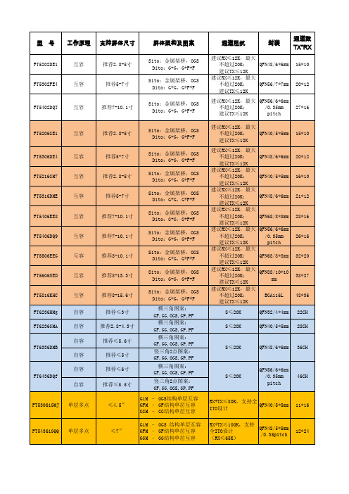
20*12
FT5402DQT
互容
推荐7-10.1寸
27*16
FT5206GE1
互容
推荐2.8-5寸
Sito:金属架桥,OGS Dito:G+G,G+F+F Sito:金属架桥,OGS Dito:G+G,G+F+F Sito:金属架桥,OGS Dito:G+G,G+F+F Sito:金属架桥,OGS Dito:G+G,G+F+F Sito:金属架桥,OGS Dito:G+G,G+F+F Sito:金属架桥,OGS Dito:G+G,G+F+F Sito:金属架桥,OGS Dito:G+G,G+F+F Sito:金属架桥,OGS Dito:G+G,G+F+F Sito:金属架桥,OGS Dito:G+G,G+F+F 横三角图案: GF,GG,OGS,GP,PF 横三角图案: GF,GG,OGS,GP,PF 横三角图案: GF,GG,OGS,GP,PF 竖三角2点图案: GF,GG,OGS,GP,PF 横三角图案: GF,GG,OGS,GP,PF 竖三角2点图案: GF,GG,OGS,GP,PF G1M – OGS结构单层互容 GFM – GF结构单层互容 GGM – GG结构单层互容 G1M – OGS 结构单层互容 GFM – GF结构单层互容 GGM – GG结构单层互容
工作电流:6mA 待机电流:4mA 睡眠电流:30uA
工作温度: -20~+85 储存温度: -55~+150 工作温度: -20~+85 储存温度: -55~+150
智能触摸芯片 CPT2610 数据手册说明书

CHIPHOMER TECHNOLOGY (SHANGHAI) LIMITEDCPT2610 数据手册单/双通道电容性触摸检测芯片September 2019目录CPT2610 数据手册 (1)目录 (2)图目录 (3)1概述 (4)2引脚 (5)2.1引脚排列 (5)2.2引脚说明 (6)3典型应用 (7)3.1双通道典型应用图 (7)3.2单通道典型应用图 (7)4功能描述 (8)4.1按键状态 (8)4.1.1按键输出有效电平选择 (8)4.1.2CPT2610SP8、CPT2610DN8 按键状态获取 (8)4.1.3CPT2610ST6、CPT2610DN6 按键状态获取 (8)4.2按键扫描模式 (8)4.3长时按键触发解除功能 (8)5电气特性 (9)6封装 (10)6.1SOP8L (10)6.2DFN2X2-8L (11)6.3SOT23-6L (12)6.4DFN1.6X1.6-6L (13)7订货信息 (14)8版本信息 (15)图目录图1CPT2610 SOP8L 引脚排列图 (5)图2CPT2610 SOT23-6L引脚排列图 (5)图3CPT2610 DFN1.6X1.6-6L引脚排列图 (5)图4CPT2610 DFN2X2-8L引脚排列图 (5)图5双通道触摸典型应用图 (7)图6单通道触摸典型应用图 (7)图7SOP8L封装尺寸图 (10)图8DFN2X2-8L封装尺寸图 (11)图9SOT23-6L封装尺寸图 (12)图10DFN1.6X1.6-6L封装尺寸图 (13)1 概述CPT2610是一款低功耗双通道/单通道电容检测芯片,具有高效的RF噪音抑制功能,能够准确识别手指触摸引起的微小电容变化,适用于用触摸按键替代机械按键等应用场合;具有实时的自校准和基线跟踪算法,能有效避免因环境因素变化而引起按键误触等情况;支持输出有效电平选择,以满足不同系统平台及应用的要求。
NESW156T-E

Rank Sbm7 x 0.3070 0.3048 0.3128 0.3150 y 0.3150 0.3198 0.3338 0.3290
Color Coordinates Measurement allowance is ± 0.005. Basically, a shipment shall consist of the LEDs of a combination of the above ranks. The percentage of each rank in the shipment shall be determined by Nichia.
点击进入洸子其科技
Nichia STS-DA1-0355A <Cat.No.090224>
(1) Absolute Maximum Ratings
Item
Symbol
Absolute Maximum Rating
Soldering Temperature
Tsld
Reflow Soldering : 260°C
Hand Soldering : 350°C
IFP Conditions : Pulse Width ≤ 10msec. and Duty ≤ 1/10
(Ta=25°C) Unit mA mA V mW °C °C
2.INITIAL OPTICAL/ELECTRICAL CHARACTERISTICS
Please refer to “CHARACTERISTICS” on the following pages.
3.OUTLINE DIMENSIONS AND MATERIALS
Please refer to “OUTLINE DIMENSIONS” on the following page.
- 1、下载文档前请自行甄别文档内容的完整性,平台不提供额外的编辑、内容补充、找答案等附加服务。
- 2、"仅部分预览"的文档,不可在线预览部分如存在完整性等问题,可反馈申请退款(可完整预览的文档不适用该条件!)。
- 3、如文档侵犯您的权益,请联系客服反馈,我们会尽快为您处理(人工客服工作时间:9:00-18:30)。
140312
= = = = = = = SSE-25640
3
6
61426-01
SANKEN ELECTRIC CO., LTD. (4) Cautions for Mounting to a Heatsink =
MN1526
0.05mm When the flatness around the screw hole is insufficient, such as when mounting the products to a heatsink that has an extruded (burred) screw hole, the products can be damaged, even with a lower than recommended screw torque. For mounting the products, the mounting surface flatness should be 0.05mm or less. =
2
For tightening screws, if a tightening tool (such as a driver) hits the products, the package may crack, and internal stress fractures may occur, which shorten the lifetime of the electrical elements and can cause catastrophic failure. Tightening with an air driver makes a substantial impact. In addition, a screw torque higher than the set torque can be applied and the package may be damaged. Therefore, an electric driver is recommended. When the package is tightened at two or more places, first pre-tighten with a lower torque at all places, then tighten with the specified torque. When using a power driver, torque control is mandatory. = 放熱板の穴径が 4mmφ 以下の場合、穴径部のプレス抜き型のダレなどは、締め付け時に樹脂部のク ラックの原因になるため注意してください。 Please pay special attention about the slack of the press mold. In case that the hole diameter of the heatsink is less than 4 mm, it may cause the resin crack at tightening.
: mm= = Dimensions in mm = DRW No.:TG3A-0101A
Epoxy resin
4-2 外観 Appearance The body shall be clean and shall not bear any stain, rust or flaw. 4-3 標示 Marking The type number and lot number shall be clearly marked in white.
When tests are carried out during inspection testing and other standard test periods, protect the products from power surges from the testing device, shorts between the product pins, and wrong connections. Ensure all test parameters are within the ratings specified by Sanken for the products. (3) Remarks About Using Silicone Grease with a Heatsink = When silicone grease is used in mounting the products on a heatsink, it shall be applied evenly and thinly. If more silicone grease than required is applied, it may produce excess stress. =
Volatile-type silicone greases may crack after long periods of time, resulting in reduced heat radiation effect. Silicone grease with low consistency (hard grease) may cause cracks in the mold resin when screwing the products to a heatsink. Our recommended silicone greases for heat radiation purposes, which will not cause any adverse effect on the product life, are indicated below: Type G746 YG6260 SC102 Suppliers Shin-Etsu Chemical Co., Ltd. Momentive Performance Materials Inc. Dow Corning Toray Co., Ltd.
Ensure that storage conditions comply with the standard temperature (5 to 35°C) and the standard relative humidity (around 40 to 75%); avoid storage locations that experience extreme changes in temperature or humidity. = Avoid locations where dust or harmful gases are present and avoid direct sunlight. = Reinspect for rust on leads and solderability of the products that have been stored for a long time. (2) Cautions for Testing and Handling
Collector-Emitter Saturation Voltage Cut-off Frequency Output Capacitance = hFE hFE rank
: 40 80(R), 50 100(O), 70
140312
= = = = = = = SSE-25640
1
6பைடு நூலகம்
61426-01
140312
= = = = = = = SSE-25640
2
6
61426-01
SANKEN ELECTRIC CO., LTD.
MN1526
5 5 Operating Precautions
OPERATING PRECAUTIONS
Because reliability can be affected adversely by improper storage environments and handling methods, please observe the following cautions. (1) Cautions for Storage = 5 35°C 40 75%
root dimension= =
root dimension= =
(1) Base (2) Collector (3) Emitter a. Description
Lead terminal Plastic body
plan= chart
side= chart
Material
Cu
Specification
Ni Ni plating, solder dip treatment Solder:Sn-3Ag-0.5Cu riV =s JM = Flammability:UL94 V-0(Equivalent)=
Type Number b. Lot Number 1st letter The last digit of year 2nd letter Month 1 9 : 10 :O 11 :N 12 :D (1 to 9 for Jan. to Sept., O for Oct. N for Nov. D for Dec.) c. hFE hFE rank
3
( 25 ) Electrical Characteristics (Ta=25 Characteristic Collector Cut-off Current Emitter Cut-off Current Collector-Emitter Voltage DC Current Transfer Ratio
Please select suitable screws for the product shape. Do not use a flat-head machine screw because of the stress to the products. Self-tapping screws are not recommended. When using self-tapping screws, the screw may enter the hole diagonally, not vertically, depending on the conditions of hole before threading or the work situation. That may stress the products and may cause failures. = Recommended Screw Torque パッケージ Package TO-220 , TO-220F TO-3P , TO-3PF , TO-247 TO-3P Wide 2Screw Type SLA = 推奨締め付けトルク Recommended Screw Torque 0.490 to 0.686 N・m 0.686 to 0.882 N・m 0.686 to 0.882 N・m 0.588 to 0.784 N・m (5 to 7 kgf・cm) (7 to 9 kgf・cm) (7 to 9 kgf・cm) (6 to 8 kgf・cm)