mb851_revc_schematic
MB85502-015资料
436 mW max. (ADD=L)
• LVTTL compatible I/O • Programmable burst type • Programmable burst length • Auto and Self-refresh • CKE power down mode • Output Enable and Input Data Mask
CLK A0 to A11 RAS
DQM
CKE
4M × 4
CS
chip 1
CAS WE
DQ DQ DQ DQ
CLK A0 to A11 RAS
DQM
CKE
4M × 4
CS
chip 2
CAS WE
DQ DQ DQ DQ
CLK A0 to A11 RAS
DQM
CKE
4M × 4
CS
chip 3
CAS WE
s ABSOLUTE MAXIMUM RATINGS (See NOTE)
Parameter Supply Voltage Input Voltage Output Voltage Short Circuit Output Current Power Dissipation Storage Temperature *1 VSS = 0 V
Ambient Oprating
Temp. 0°C to +70 °C
s CAPACITANCE
Parameter Input Capacitance, A0 to A11 Input Capacitance, RAS, CAS, WE Input Capacitance, CLK Input Capacitance, DQM0, DQM1 Input Capacitance, CKE0, CKE1 Input Capacitance, CS0, CS1 I/O Capacitance, (DQ0 to DQ35)
MAX8510 MAX8511 MAX8512 极低噪声、低掉电的线性调压器说明说明书

General DescriptionThe MAX8510/MAX8511/MAX8512 ultra-low-noise, low-dropout (LDO) linear regulators are designed to deliver up to 120mA continuous output current. These regulators achieve a low 120mV dropout for 120mA load current. The MAX8510 uses an advanced architecture to achieve ultra-low output voltage noise of 11μV RMS and PSRR of 54dB at 100kHz.The MAX8511 does not require a bypass capacitor, hence achieving the smallest PC board area. The MAX8512’s output voltage can be adjusted with an external divider.The MAX8510/MAX8511 are preset to a variety of voltag-es in the 1.5V to 4.5V range. Designed with a P-channel MOSFET series pass transistor, the MAX8510/MAX8511/MAX8512 maintain very low ground current (40μA).The regulators are designed and optimized to work with low-value, low-cost ceramic capacitors. The MAX8510 requires only 1μF (typ) of output capacitance for stability with any load. When disabled, current consumption drops to below 1μA.Package options include a 5-pin SC70 and a tiny 2mm x 2mm x 0.8mm TDFN package.Applications●Cellular and Cordless Phones ●PDA and Palmtop Computers ●Base Stations●Bluetooth Portable Radios and Accessories ●Wireless LANs ●Digital Cameras ●Personal Stereos●Portable and Battery-Powered EquipmentFeatures●Space-Saving SC70 and TDFN (2mm x 2mm) Packages ●11μV RMS Output Noise at 100Hz to 100kHzBandwidth (MAX8510)●78dB PSRR at 1kHz (MAX8510) ●120mV Dropout at 120mA Load●Stable with 1μF Ceramic Capacitor for Any Load ●Guaranteed 120mA Output●Only Need Input and Output Capacitors (MAX8511) ●Output Voltages: 1.5V, 1.8V, 2.5V, 2.6V, 2.7V, 2.8V,2.85V, 3V,3.3V,4.5V (MAX8510/MAX8511) and Adjustable (MAX8512) ●Low 40μA Ground Current ●Excellent Load/Line Transient●Overcurrent and Thermal Protection19-2732; Rev 5; 5/19Output Voltage Selector Guide appears at end of data sheet.Ordering Information continued at end of data sheet.*xy is the output voltage code (see Output Voltage Selector Guide). Other versions between 1.5V and 4.5V are available in 100mV increments. Contact factory for other versions.+Denotes a lead(Pb)-free/RoHS-compliant package.T = Tape and reel.PART*TEMP RANGE PIN-PACKAGEMAX8510EXKxy+T -40°C to +85°C 5 SC70MAX8510/MAX8511/MAX8512Ultra-Low-Noise, High PSRR,Low-Dropout, 120mA Linear RegulatorsOrdering InformationClick here for production status of specific part numbers.IN to GND ................................................................-0.3V to +7V Output Short-Circuit Duration ...........................................Infinite OUT, SHDN to GND .....................................-0.3V to (IN + 0.3V)FB, BP , N.C. to GND ................................-0.3V to (OUT + 0.3V)Continuous Power Dissipation (T A = +70°C)5-Pin SC70 (derate 3.1mW/°C above +70°C) .............0.247W 8-Pin TDFN (derate 11.9mW/°C above = 70°C) .........0.953W Operating Temperature Range ...........................-40°C to +85°CMilitary Operating Temperature Range .............-55°C to +110°C Junction Temperature ......................................................+150°C Storage Temperature Range ............................-65°C to +150°C Lead Temperature (soldering, 10s) .................................+300°C Soldering Temperature (reflow) .......................................+260°C Lead (Pb)-free packages .................................................+260°C Packages containing lead (Pb) .......................................+240°C(Note 1)SC70Junction-to-Ambient Thermal Resistance (θJA ) ........324°C/W Junction-to-Case Thermal Resistance (θJC ) .............115°C/WTDFNJunction-to-Ambient Thermal Resistance (θJA ) .......83.9°C/W Junction-to-Case Thermal Resistance (θJC ) ...............37°C/W(V IN = V OUT + 0.5V, T A = -40°C to +85°C, unless otherwise noted. C IN = 1μF, C OUT = 1μF, C BP = 10nF. Typical values are at +25°C; the MAX8512 is tested with 2.45V output, unless otherwise noted.) (Note 2)PARAMETER SYMBOL CONDITIONSMIN TYPMAX UNITS Input Voltage Range V IN26VOutput Voltage Accuracy I OUT = 1mA, T A = +25°C-1+1%I OUT = 100µA to 80mA, T A = +25°C -2+2I OUT = 100µA to 80mA-3+3Maximum Output Current I OUT 120mA Current LimitI LIMV OUT = 90% of nominal value 130200300mA Dropout Voltage (Note 3)V OUT ≥ 3V, I OUT = 80mA 80170mVV OUT ≥ 3V, I OUT = 120mA1202.5V ≤ V OUT < 3V, I OUT = 80mA 902002.5V ≤ V OUT < 3V, I OUT = 120mA 1352V ≤ V OUT < 2.5V, I OUT = 80mA 1202502V ≤ V OUT < 2.5V, I OUT = 120mA180Ground Current I Q I OUT = 0.05mA4090µA V IN = V OUT (nom) - 0.1V, I OUT = 0mA 220500Line Regulation V LNR V IN = (V OUT + 0.5V) to 6V, I OUT = 0.1mA 0.001%/V Load RegulationV LDR I OUT = 1mA to 80mA 0.003%/mA Shutdown Supply CurrentI SHDNV SHDN = 0VT A = +25°C 0.0031µAT A = +85°C 0.05Ripple RejectionPSRRf = 1kHz, I OUT = 10mAMAX851078dBMAX8511/MAX851272f = 10kHz, I OUT = 10mA MAX851075MAX8511/MAX851265f = 100kHz, I OUT = 10mAMAX851054MAX8511/ MAX851246MAX8512Low-Dropout, 120mA Linear RegulatorsAbsolute Maximum RatingsStresses beyond those listed under “Absolute Maximum Ratings” may cause permanent damage to the device. These are stress ratings only, and functional operation of the device at these or any other conditions beyond those indicated in the operational sections of the specifications is not implied. Exposure to absolute maximum rating conditions for extended periods may affect device reliability.Electrical CharacteristicsPackage Thermal Characteristics Note 1: Package thermal resistances were obtained using the method described in JEDEC specification JESD51-7, using a four-layerboard. For detailed information on package thermal considerations, refer to /thermal-tutorial .(V IN = V OUT + 0.5V, T A = -40°C to +85°C, unless otherwise noted. C IN = 1μF, C OUT = 1μF, C BP = 10nF. Typical values are at +25°C; the MAX8512 is tested with 2.45V output, unless otherwise noted.) (Note 2)Note 2: Limits are 100% tested at +25°C. Limits over operating temperature range are guaranteed by design.Note 3: Dropout is defined as V IN - V OUT when V OUT is 100mV below the value of V OUT for V IN = V OUT + 0.5V.Note 4: Time needed for V OUT to reach 90% of final value.(V IN = V OUT + 0.5V, C IN = 1μF, C OUT = 1μF, C BP = 10nF, T A = +25°C, unless otherwise noted.)PARAMETER SYMBOLCONDITIONSMINTYP MAXUNITSOutput Noise Voltage (RMS)f = 100Hz to 100kHz, I LOAD = 10mA MAX851011µVMAX8511/MAX8512230f = 100Hz to 100kHz, I LOAD = 80mA MAX851013MAX8511/MAX8512230Shutdown Exit Delay R LOAD = 50Ω (Note 4)300µs SHDN Logic Low Level V IN = 2V to 6V 0.4V SHDN Logic High Level V IN = 2V to 6V 1.5V SHDN Input Bias Current V IN = 6V, V SHDN = 0V or 6VT A = +25°C µA T A = +85°C 0.01FB Input Bias Current (MAX8512)V IN = 6V,V FB = 1.3VT A = +25°C 0.0060.1µA T A = +85°C0.01Thermal Shutdown 160°C Thermal-Shutdown Hysteresis10°C MAX8510OUTPUT VOLTAGE ACCURACYvs. LOAD CURRENTM A X 8510 t o c 02LOAD CURRENT (mA)% D E V I A T I O N (%)10080604020-0.4-0.200.20.40.6-0.60120MAX8510OUTPUT VOLTAGE ACCURACYvs. TEMPERATURETEMPERATURE (°C)% D E V I A T I O N (%)603510-15-0.8-0.6-0.4-0.200.20.40.60.81.0-1.0-4085MAX8510OUTPUT VOLTAGE vs. INPUT VOLTAGEINPUT VOLTAGE (V)O U T P U T V O L T A G E (V )543210.51.01.52.02.53.00.06MAX8512Low-Dropout, 120mA Linear RegulatorsElectrical Characteristics (continued)Typical Operating Characteristics(V IN = V OUT + 0.5V, C IN = 1μF, C OUT = 1μF, C BP = 10nF, T A = +25°C, unless otherwise noted.)MAX8510DROPOUT VOLTAGE vs. OUTPUT VOLTAGEOUTPUT (V)D R O P O U T V O L T A G E (m V )3.02.82.62.42.2501001502002502.03.2MAX8510GROUND PIN CURRENT vs. TEMPERATUREM A X 8510 t o c 08TEMPERATURE (°C)G R O U N D P I N C U R R E N T (µA )603510-153540455030-4085MAX8510OUTPUT NOISE400µs/divMAX8510GROUND PIN CURRENT vs. INPUT VOLTAGEINPUT VOLTAGE (V)G R O U N D P I N C U R R E N T (µA )43211502005010025030035005MAX8510PSRR vs. FREQUENCYFREQUENCY (kHz)P S R R (d B )1101000.14050601020307080900.011000MAX8510OUTPUT NOISE SPECTRAL DENSITYvs. FREQUENCYMAX8510 toc12FREQUENCY (kHz)O U T P U T N O I S E D E N S I T Y (n V /H z )0.11101001.E+031.E+021.E+041.E+010.011000MAX8510DROPOUT VOLTAGE vs. LOAD CURRENTLOAD CURRENT (mA)D R O P O U T V O L T A G E (m V )1008060402030609012015000120MAX8510GROUND PIN CURRENT vs. LOAD CURRENTLOAD CURRENT (mA)G R O U N D P I N C U R R E N T (µA )10080604020408012016020024000120MAX8511PSRR vs. FREQUENCYFREQUENCY (kHz)P S R R (d B )0.111010040506010203070809000.011000MAX8512Low-Dropout, 120mA Linear RegulatorsTypical Operating Characteristics (continued)(V IN = V OUT + 0.5V, C IN = 1μF, C OUT = 1μF, C BP = 10nF, T A= +25°C, unless otherwise noted.)MAX8510LOAD TRANSIENT RESPONSE1ms/div V OUT 10mV/divMAX8510EXITING SHUTDOWN WAVEFORM20µs/divV OUT = 2.85VR LOAD = 47ΩOUTPUT VOLTAGE 2V/divSHUTDOWN VOLTAGEMAX8510LOAD TRANSIENT RESPONSE NEAR DROPOUT1ms/divV OUT 10mV/divMAX8510ENTERING SHUTDOWN DELAY40µs/divC BP = 0.01µFOUTPUT VOLTAGE 2V/divSHUTDOWN VOLTAGEMAX8510REGION OF STABLE C OUT ESRvs. LOAD CURRENTM A X 8510 t o c 20LOAD CURRENT (mA)C O U T E S R (Ω)806040200.11101000.01120100STABLE REGIONMAX8510OUTPUT NOISE vs. BP CAPACITANCEM A X 8510 t o c 13BP CAPACITANCE (nF)O U T P U T N O I S E (µV )1051015202501100MAX8510LINE TRANSIENT RESPONSE200µs/divV IN = 3.5V TO 4VV OUT 2mV/divMAX8510SHUTDOWN EXIT DELAY20µs/divV OUT 1V/divSHUTDOWN VOLTAGEV OUT = 3V C BP = 100nFMAX8512Low-Dropout, 120mA Linear RegulatorsTypical Operating Characteristics (continued)Detailed DescriptionThe MAX8510/MAX8511/MAX8512 are ultra-low-noise, low-dropout, low-quiescent current linear regulators designed for space-restricted applications. The parts are available with preset output voltages ranging from 1.5V to 4.5V in 100mV increments. These devices can supply loads up to 120mA. As shown in the Functional Diagram , the MAX8510/MAX8511 consist of an innovative bandgap core and noise bypass circuit, error amplifier, P-channel pass transistor, and internal feedback voltage-divider. The MAX8512 allows for adjustable output with an external feedback network.The 1.225V bandgap reference is connected to the error amplifier’s inverting input. The error amplifier compares this reference with the feedback voltage and amplifies the difference. If the feedback voltage is lower than the refer-ence voltage, the pass-transistor gate is pulled low. This allows more current to pass to the output and increases the output voltage. If the feedback voltage is too high, the pass transistor gate is pulled high, allowing less cur-rent to pass to the output. The output voltage is fed back through an internal resistor voltage-divider connected to the OUT pin.An external bypass capacitor connected to BP (MAX8510) reduces noise at the output. Additional blocks include a current limiter, thermal sensor, and shutdown logic.Internal P-Channel Pass TransistorThe MAX8510/MAX8511/MAX8512 feature a 1Ω (typ) P-channel MOSFET pass transistor. This provides sev-eral advantages over similar designs using a PNP pass transistor, including longer battery life. The P-channel MOSFET requires no base drive, which considerably reduces quiescent current. PNP-based regulators waste considerable current in dropout when the pass transistor saturates. They also use high base-drive current under heavy loads. The MAX8510/MAX8511/MAX8512 do not suffer from these problems and consume only 40μA of quiescent current in light load and 220μA in dropout (see the Typical Operating Characteristics ).Output Voltage SelectionThe MAX8510/MAX8511 are supplied with factory-set output voltages from 1.5V to 4.5V, in 100mV increments (see Ordering Information ). The MAX8512 features a user-adjustable output through an external feedback net-work (see the Typical Operating Circuits ).To set the output of the MAX8512, use the following equa-tion:OUT REF V R1R2X -1V=where R2 is chosen to be less than 240kΩ and V REF = 1.225V. Use 1% or better resistors.PINNAMEFUNCTIONMAX8510MAX8511MAX8512SC70TDFN -EP SC70TDFN -EP SC70TDFN -EP 151515IN Unregulated Input Supply 232323GNDGround343434SHDN Shutdown. Pull low to disable the regulator.42————BP Noise Bypass for Low-Noise Operation. Connect a 10nF capacitor from BP to OUT. BP is shorted to OUT in shutdown mode.————42FB Adjustable Output Feedback Point575757OUT Regulated Output Voltage. Bypass with a capacitor to GND. See the Capacitor Selection and Regulator Stability section for more details.—1, 6, 841, 2, 6,—1, 6, 8N.C.No connection. Not internally connected.——————EPExposed Pad (TDFN Only). Internally connected to GND. Connect to a large ground plane to maximize thermal performance. Not intended as an electrical connection point.MAX8512Low-Dropout, 120mA Linear RegulatorsPin DescriptionShutdownThe MAX8510/MAX8511/MAX8512 feature a low-power shutdown mode that reduces quiescent current less than 1μA. Driving SHDN low disables the voltage reference, error amplifier, gate-drive circuitry, and pass transistor (see the Functional Diagram), and the device output enters a high-impedance state. Connect SHDN to IN for normal operation.Current LimitThe MAX8510/MAX8511/MAX8512 include a current lim-iter, which monitors and controls the pass transistor’s gate voltage, limiting the output current to 200mA. For design purposes, consider the current limit to be 130mA (min) to 300mA (max). The output can be shorted to ground for an indefinite amount of time without damaging the part. Thermal-Overload ProtectionThermal-overload protection limits total power dissipation in the MAX8510/MAX8511/MAX8512. When the junction temperature exceeds T J = +160°C, the thermal sensor signals the shutdown logic, turning off the pass transis-tor and allowing the IC to cool down. The thermal sensor turns the pass transistor on again after the IC’s junction temperature drops by 10°C, resulting in a pulsed output during continuous thermal-overload conditions.Thermal-overload protection is designed to protect the MAX8510/MAX8511/MAX8512 in the event of a fault con-dition. For continual operation, do not exceed the abso-lute maximum junction temperature rating of T J = +150°C. Operating Region and Power DissipationThe MAX8510/MAX8511/MAX8512 maximum power dis-sipation depends on the thermal resistance of the case and circuit board, the temperature difference between the die junction and ambient, and the rate of airflow. The power dissipation across the device is:P = I OUT (V IN - V OUT)The maximum power dissipation is:P MAX = (T J - T A) / (θJC + θCA)where T J - T A is the temperature difference between the MAX8510/MAX8511/MAX8512 die junction and the sur-rounding air, θJC is the thermal resistance of the package, and θCA is the thermal resistance through the PC board, copper traces, and other materials to the surrounding air. The GND pin of the MAX8510/MAX8511/MAX8512 per-forms the dual function of providing an electrical connec-tion to ground and channeling heat away. Connect the GND pin to ground using a large pad or ground plane.Noise ReductionFor the MAX8510, an external 0.01μF bypass capaci-tor between BP and OUT with innovative noise bypass scheme reduces output noises dramatically, exhibiting 11μV RMS of output voltage noise with C BP = 0.01μF and C OUT = 1μF. Startup time is minimized by a poweron cir-cuit that precharges the bypass capacitor. Applications InformationCapacitor Selectionand Regulator StabilityUse a 1μF capacitor on the MAX8510/MAX8511/MAX8512 input and a 1μF capacitor on the output. Larger input capacitor values and lower ESRs provide better noise rejection and line-transient response. Reduce output noise and improve load-transient response, stability, and power-supply rejection by using large output capacitors. Note that some ceramic dielectrics exhibit large capaci-tance and ESR variation with temperature. With dielec-trics such as Z5U and Y5V, it may be necessary to use a 2.2μF or larger output capacitor to ensure stability at temperatures below -10°C. With X7R or X5R dielectrics, 1μF is sufficient at all operating temperatures. A graph of the region of stable C OUT ESR vs. load current is shown in the Typical Operating Characteristics.Use a 0.01μF bypass capacitor at BP (MAX8510) for low-output voltage noise. The leakage current going into the BP pin should be less than 10nA. Increasing the capaci-tance slightly decreases the output noise. Values above 0.1μF and below 0.001μF are not recommended. Noise, PSRR, and Transient ResponseThe MAX8510/MAX8511/MAX8512 are designed to deliv-er ultra-low noise and high PSRR, as well as low dropout and low quiescent currents in battery-powered systems. The MAX8510 power-supply rejection is 78dB at 1kHz and 54dB at 100kHz. The MAX8511/MAX8512 PSRR is 72dB at 1kHz and 46dB at 100kHz (see the Power-Supply Rejection Ratio vs. Frequency graph in the Typical Operating Characteristics).When operating from sources other than batteries, improved supply-noise rejection and transient response can be achieved by increasing the values of the input and output bypass capacitors, and through passive filter-ing techniques. The Typical Operating Characteristics show the MAX8510/MAX8511/MAX8512 line- and load-transient responses.MAX8512Low-Dropout, 120mA Linear RegulatorsDropout VoltageA regulator’s minimum dropout voltage determines the lowest usable supply voltage. In battery-powered sys-tems, this determines the useful end-of-life battery volt-age. Because the MAX8510/MAX8511/MAX8512 use aP-channel MOSFET pass transistor, their dropout voltage is a function of drain-to-source on-resistance (RDS(ON)) multiplied by the load current (see the Typical Operating Characteristics ).MAX8512Low-Dropout, 120mA Linear RegulatorsFunctional Diagram*xy is the output voltage code (see Output Voltage Selector Guide). Other versions between 1.5V and 4.5V are available in 100mV increments. Contact factory for other versions.**EP = Exposed pad.+Denotes a lead(Pb)-free/RoHS-compliant package.T = Tape and reel.(Note: Standard output voltage options, shown in bold , are available. Contact the factory for other output voltages between 1.5V and 4.5V. Minimum order quantity is 15,000 units.)PART*TEMP RANGE PIN-PACKAGE MAX8510MXK33/PR3+-55°C to +110°C 5 SC70MAX8510ETAxy+T -40°C to +85°C 8 TDFN-EP** 2mm x 2mm MAX8511EXKxy+T -40°C to +85°C 5 SC70MAX8511ETAxy+T -40°C to +85°C 8 TDFN-EP** 2mm x 2mm MAX8512EXK+T -40°C to +85°C 5 SC70MAX8512ETA+T-40°C to +85°C8 TDFN-EP** 2mm x 2mmPARTV OUT (V)TOP MARKMAX8510EXK16+T 1.6AEX MAX8510EXK18+T 1.8AEA MAX8510ETA25+T 2.5AAO MAX8510EXK27+T 2.7ATD MAX8510ETA28+T 2.8AAR MAX8510EXK29+T 2.85ADS MAX8510MXK33/PR3+ 3.3AUV MAX8510ETA30+T 3AAS MAX8510ETA33+T 3.3AAT MAX8510ETA45+T 4.5AAU MAX8510MXK33/PR3+ 3.3AUV MAX8511EXK15+T 1.5ADU MAX8511ETA18+T 1.8AAV MAX8511ETA25+T 2.5AAP MAX8511ETA26+T 2.6AAW MAX8511EXK28+T 2.8AFA MAX8511ETA29+T 2.85AAX MAX8511EXK89+T 2.9AEH MAX8511EXK31+T 3.1ARS MAX8511ETA33+T 3.3AAY MAX8511EXK45+T4.5AEJ MAX8512ETA+TAdjustableAAQPACKAGE TYPE PACKAGE CODE OUTLINE ND PATTERN NO.8 TDFN T822+121-016890-00645 SC70X5+121-007690-0188MAX8512Low-Dropout, 120mA Linear RegulatorsTypical Operating Circuits (continued)Ordering Information (continued)Output Voltage Selector GuidePackage InformationFor the latest package outline information and land patterns (footprints), go to /packages . Note that a “+”, “#”, or “-” in the package code indicates RoHS status only. Package drawings may show a different suffix character, but the drawing pertains to the package regardless of RoHS status.Chip InformationPROCESS: BiCMOSREVISION NUMBERREVISION DATE DESCRIPTIONPAGES CHANGED 48/11Corrected errors and added lead-free packages 1, 2, 3, 6, 955/19Updated Output Voltage Selector Guide9Maxim Integrated cannot assume responsibility for use of any circuitry other than circuitry entirely embodied in a Maxim Integrated product. No circuit patent licenses are implied. Maxim Integrated reserves the right to change the circuitry and specifications without notice at any time. The parametric values (min and max limits) shown in the Electrical Characteristics table are guaranteed. Other parametric values quoted in this data sheet are provided for guidance.MAX8512Low-Dropout, 120mA Linear RegulatorsRevision HistoryFor pricing, delivery, and ordering information, please visit Maxim Integrated’s online storefront at https:///en/storefront/storefront.html.。
RPM851中文资料

RPM851A Series
FApplication example
655
元器件交易网 Communication ICs
FRecommended values (at VCC = 3V)
RPM851A Series
656
元器件交易网 Communication ICs
FOptical characteristics (unless otherwise noted, LEDVCC = VCC = PDVCC = 3V, Ta = 25_C)
Байду номын сангаас654
元器件交易网 Communication ICs
FCircuit operation Timing charts
RPM851A Series
S Better to be placed more than 1.0cm in radius from photo diode (pin13) and also away from the parts which generates noise, such as DC / DC converter. Digital signal line, such as clock pulse, bus etc, are also away more than 1.0cm in radius from photo diode. S As for C1, C2 and, GND should be close to pin7 and placed close to pins11, 12 and 13 (within 5mm). (3) Please be sure to set up the TXD (pin6) input to be “L” (under 0.5 [V]) except transmitting data (for < 90 µ s. ON Duty < 20%). (4) Powerdown current might increase if exposed by strong light (ex. direct sunlight) at powerdown mode. (5) Please use by the signal form which is specified by IrDA Ver1.0. There might be on error if used by different signal form.
低电压检测器BL8518产品说明书
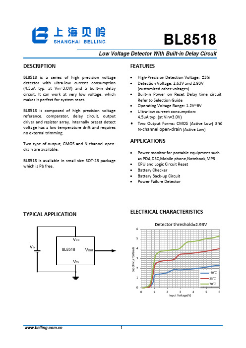
Low Voltage Detector With Built-in Delay CircuitBL8518DESCRIPTIONBL8518 is a series of high precision voltage detector with ultra-low current consumption (4.5uA typ. at Vin=3.0V) and a built-in delay circuit. It can work at very low voltage, which makes it perfect for system reset.BL8518 is composed of high precision voltage reference, comparator, delay circuit, output driver and resistor array. Internally preset detect voltage has a low temperature drift and requires no external trimming.Two type of output, CMOS and N-channel open-drain are available.BL8518 is available in small size SOT-23 package which is Pb free.FEATURES∙ High-Precision Detection Voltage: ±3% ∙ Detection Voltage: 2.63V and 2.93V(customized other voltages)∙ Built-in Power on Reset Delay time circuit:Refer to Selection Guide∙ Operating Voltage Range: 1.2V~6V ∙ Ultra-low current consumption:4.5uA typ. (at Vin=3.0V)∙ Two Output Forms: CMOS (Active Low) and N-channel open-drain (Active Low)APPLICATIONS∙ Power monitor for portable equipment suchas PDA,DSC,Mobile phone,Notebook,MP3 ∙ CPU and Logic Circuit Reset ∙ Battery Checker∙ Battery Back-up Circuit ∙ Power Failure DetectorTYPICAL APPLICATIONVELECTRICAL CHARACTERISTICS0 123 4 56123 456S u p p l y c u r r e n t (u A )Input Voltage(V)Detector threshold=2.93V-40℃25℃ 70℃ORDERING INFORMATION123456ABSOLUTE MAXIMUM RATINGNote:Exceed these limits to damage to the device.Exposure to absolute maximum rating conditions may affect device reliability. RECOMMENDED WORK CONDITIONSELECTRICAL CHARACTERISTICSBL8518CXXTR263DC/N(2.63V)BL8518CXXTR293DC/N(2.93V)ELECTRICAL CHARACTERISTICS BY OUTPUT DELAY TIMEBLOCK DIAGRAMVoutV DDN Channel Open DrainVssVoutV DDCMOS OutputFUNCTION DESCRIPTIONVssVoutDDHigh precision low temperature co-efficiency reference voltage is applied to the negative input of a comparator. Input voltage, divided by resistor array of Ra and Rb, is applied to the positive input of the comparator. Output of the comparator passes a delay circuit and a series of buffer to drive the output CMOS pair.VDET =VREF*(1+Ra/Rb)VssVssTEST CIRCUITS(1) Supply current test circuit(2) Detector threshold test circuitV SSVOUTLC9018V DDV INV OUT(3) NCH Drive Output Current Test Circuit(4) PCH Drive Output Current Test CircuitV V DSV - V DSDDBL8518BL8518TYPICAL PERFORMANCE CHARACTERISTICS1) Supply current VS. Input voltage3) Nch Driver Output Current VS. VDS5) PCH Driver Output Current vs. Input Current4) NCH Driver Output Current vs. Input Voltage0 1 23 4 5 6 0123 456S u p p l y c u r r e n t (u A )Input Voltage(V)Detector threshold=2.93V-40℃25℃ 70℃0 2 4 6 8 10 12 14 16 18 20 0.00.51.01.52.02.53.0O u t p u t C u r r e n t (m A )VDS(V)Detector threshold=2.93VVDD=2V VDD=1V 0 5101520 25123 4O u t p u t C u r r e n t (m A )Input Voltage Vin(V)Detector threshold=2.93V-40℃ 25℃ 70℃0 5 10 15 20 25 30 35 40 0123 4 5 67O u t p u t C u r r e n t (m A )Input Voltage Vin(V)Detector threshold=2.93VVds=0.5V Vds=1.0V Vds=1.5V Vds=2.0VPACKAGE LINE。
BM85调试
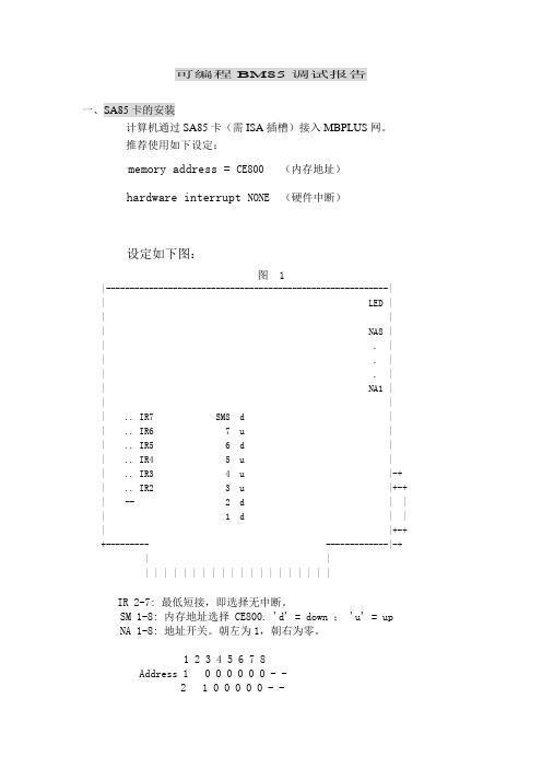
可编程BM85调试报告一、SA85卡的安装计算机通过SA85卡(需ISA插槽)接入MBPLUS网。
推荐使用如下设定:memory address = CE800 (内存地址)hardware interrupt NONE (硬件中断)设定如下图:图 1|-----------------------------------------------------------|| LED || || NA8 || . || . || . || NA1 || || .. IR7 SM8 d || .. IR6 7 u || .. IR5 6 d || .. IR4 5 u || .. IR3 4 u |-+ | .. IR2 3 u |+-+ | -- 2 d | | | 1 d | | | |+-+ +--------- -------------|-+ | || | | | | | | | | | | | | | | | | | | |IR 2-7: 最低短接,即选择无中断。
SM 1-8: 内存地址选择 CE800. 'd' = down ; 'u' = up NA 1-8: 地址开关。
朝左为1,朝右为零。
1 2 3 4 5 6 7 8Address 1 0 0 0 0 0 0 - -2 1 0 0 0 0 0 - -3 0 1 0 0 0 0 - -4 1 1 0 0 0 0 - -. . . . . . . . . .63 0 1 1 1 1 1 - -64 1 1 1 1 1 1 - -SA85卡的驱动程序有16位和32位两种。
此次调试在NT Workstation4.0上进行。
由于下载软件bm85load.exe需要16位驱动程序(在DOS下格式为:bm85load /s5c /re000 /p4.4 bm85.exe) 。
所以需安装SA85卡的16位驱动程序。
851-300 Rev. B 设备说明书

851-300 Rev. BSet-up, Operation& Maintenance ManualTable of ContentsWarnings – General Safety 2. . . . . . . . . . . . . . . . . . . . Introduction 2. . . . . . . . . . . . . . . . . . . . . . . . . . . . . . . . Product Description 3. . . . . . . . . . . . . . . . . . . . . . . . . . Specifications 3. . . . . . . . . . . . . . . . . . . . . . . . . . . . . . . Installation 4. . . . . . . . . . . . . . . . . . . . . . . . . . . . . . . . . Required Tools 4. . . . . . . . . . . . . . . . . . . . . . . . . . . . Mounting 4. . . . . . . . . . . . . . . . . . . . . . . . . . . . . . . . Preventative Maintenance & Adjustment 6. . . . . . . . . Required Tools 6. . . . . . . . . . . . . . . . . . . . . . . . . . . . Timing Belt Tensioning 6. . . . . . . . . . . . . . . . . . . . . Timing Belt Replacement 6. . . . . . . . . . . . . . . . . . . Drive or Driven Pulley Replacement 7. . . . . . . . . . . Gearmotor Replacement 7. . . . . . . . . . . . . . . . . . . . Service Parts 9. . . . . . . . . . . . . . . . . . . . . . . . . . . . . . . Return Policy 10. . . . . . . . . . . . . . . . . . . . . . . . . . . . . .2100, 4100, 6100 Series Bottom Mount Drive Package for Light Load 50 Hz Gearmotors SOMM851-300 Rev. B 2Dorner Mfg. Corp.IntroductionIMPORTANT: Some illustrations may showguards removed. Do NOT operate equipment with-out guards.Upon receipt of shipment:D Compare shipment with packing slip. Contact factory regarding discrepancies.D Inspect packages for shipping damage. Contact carrier regarding damage.D Accessories may be shipped loose. See accessory in-structions for installation.Dorner 2100 Series conveyors are covered by the following patent numbers: 5131529, 5174435, and corresponding patents and patent applications in other countries.Dorner 4100 Series conveyors are covered by patent number 3923148 and corresponding patents and patent applications in other countries.Dorner 6100 Series conveyors are covered by patent number 5174435 and corresponding patents and patent applications in other countries.Dorner ’s Limited Warranty applies.Dorner reserves the right to make changes at any time without notice or obligation.Warnings – General Safety2100, 4100, 6100 Series Bottom Mount Drive Package for Light Load 50 Hz Gearmotors SOMMDorner Mfg. Corp.3851-300 Rev. BRefer to Figure 1 for typical components.A ConveyorB Mounting BracketC GearmotorD Belt TensionerE CoverF Timing BeltG Drive Pulley HDriven PulleyTypical ComponentsFigure 1ABCDEFG H SpecificationsGearmotor Mounting Package Models:Example:4 = 4100 Series Conveyor 6 = 6100 Series Conveyor– = flat belt, A through J = cleated belt )Driven Pulley (see Table 2)* See “Ordering and Specifications ” Catalog for details.Table 1: Gearmotor SpecificationsProduct Description2100, 4100, 6100 Series Bottom Mount Drive Package for Light Load 50 Hz Gearmotors SOMM851-300 Rev. B 4Dorner Mfg. Corp.Table 2: Belt Speeds for Light Load Fixed Speed Parallel Shaft 50 Hz Gearmotors(vp) = voltage and phase 21 = 230 V, 1-phase 23 = 230 V, 3-phase 43 = 400 V, 3-phaseNOTE: 203 through 610 mm wide conveyors withlight load drives should be limited to 2438 mm length.NOTE: For belt speed other than those listed, con-tact factory for details.InstallationRequired ToolsD Hex key wrenches:2.5 mm, 3 mm & 5 mm D Straight edge D Torque wrenchInstallation Component ListI Bottom Mount Assembly J Driven Pulley K CoverL M4 Socket Head Screws (4x)M Timing Belt N KeyOM6 Socket Head Screws (2x)Mounting1.Typical components (Figure 2)Figure 2NKMJLOISpecifications2100, 4100, 6100 Series Bottom Mount Drive Package for Light Load 50 Hz Gearmotors SOMMDorner Mfg. Corp.5851-300 Rev. BNOTE: 6100 conveyor shown, 2100 & 4100 similar.2.Locate drive output shaft (P of Figure 3) and removetwo (2) screws (Q).Figure 3QP3.Attach mount assembly (I of Figure 4) with screws(O). Tighten screws to 9 Nm.Figure 4OI4.Install key (N of Figure 5).Figure 5NRM5.Wrap timing belt (M) around driven pulley (J) anddrive pulley (R). Install driven pulley (J) onto conveyor shaft.ing a straight edge (S of Figure 6), align drivenpulley (J) with drive pulley (R). Tighten driven pulley set screws (T).Figure 6SJTR7.Depending on conveyor belt travel (direction 1 or 2),locate timing belt tensioner (U of Figure 7) as shown.Tension timing belt to obtain 3 mm deflection for 456grams of force at timing belt mid-point (V). Tightentensioner screw to 12 Nm.21VUFigure 78.Install cover (K of Figure 8) with four (4) screws (L).Tighten to 4 Nm.Figure 8KLLInstallation2100, 4100, 6100 Series Bottom Mount Drive Package for Light Load 50 Hz Gearmotors SOMM851-300 Rev. B 6Dorner Mfg. Corp.Required ToolsD Hex key wrenches:2.5 mm, 3 mm, 5 mm D Straight edgeD Screwdriver (for terminal box screws)D Torque wrenchTiming Belt Tensioning1.Remove four (4) screws (L of Figure 9) and removecover (K).Figure 9KLL2.Loosen tensioner (U of Figure 10).Figure 10U3.Depending on conveyor belt travel (direction 1 or 2),locate timing belt tensioner (U of Figure 11) as shown.Tension timing belt to obtain 3 mm deflection for 456grams of force at timing belt mid-point (V). Tighten tensioner screw to 12 Nm.21VUFigure 114.Install cover (K of Figure 9) with four (4) screws (L).Tighten screws to 4 Nm.Timing Belt Replacement1.Remove four (4) screws (L of Figure 9) and removecover (K).2.Loosen tensioner (U of Figure 10).3.Remove timing belt (M of Figure 12).NOTE: If timing belt does not slide over pulleyflange, loosen driven pulley set screws (T of Figure 12) and remove pulley with belt. For re-installation,see steps 5 through 8 on page 5.Figure 12TM4.Install new timing belt.Preventive Maintenance and Adjustment2100, 4100, 6100 Series Bottom Mount Drive Package for Light Load 50 Hz Gearmotors SOMMDorner Mfg. Corp.7851-300 Rev. B5.Depending on conveyor belt travel (direction 1 or 2),locate timing belt tensioner (U of Figure 11) as shown. Tension timing belt to obtain 3 mm deflection for 456 grams of force at timing belt mid-point (V). Tighten tensioner screw to 12 Nm.6.Install cover (K of Figure 9) with four (4) screws (L).Tighten screws to 4 Nm.Drive or Driven Pulley Replacementplete steps 1 through 3 of “Timing BeltReplacement ” section on page 6.2.Loosen set screws and remove drive or driven pulley.NOTE: If drive pulley (R of Figure 13) is replaced,wrap timing belt (M) around drive pulley and complete step 3.Figure 13Mplete steps 5 through 8 of “Installation ” sectionon page 5.Gearmotor ReplacementNOTE: Single phase gearmotor shown, three phasesimilar.1.For single phase motor:a .Loosen terminal box screws (W of Figure 14) andremove cover (X).Figure 14WXPreventive Maintenance and Adjustment2100, 4100, 6100 Series Bottom Mount Drive Package for Light Load 50 Hz Gearmotors SOMM851-300 Rev. B 8Dorner Mfg. Corp.b .(Figure 15). Loosen terminals U1, W1and ground and remove wires.Figure 15c .Loosen cord grip (Y of Figure 15) and removecord.1.For three phase motor:a .Loosen terminal box screws (W of Figure 14) andremove cover (X).b .(Figure 16). Loosen terminals U1, V1,W1 and ground and remove wires.Figure 16c .Loosen cord grip (Y of Figure 16) and removecord.2.Remove four (4) screws (L of Figure 9) and remove cover (K).3.Loosen tensioner (U of Figure 10).4.Remove timing belt (M of Figure 12).NOTE: If timing belt does not slide over pulleyflange, loosen driven pulley set screws (T of Figure 17) and remove pulley with belt (M). For re-installation, see steps 5 through 8 on page 5.Figure 17TM5.Loosen two (2) set screws (T of Figure 18). Removedrive pulley (R).Figure 18ADADRT6.Remove four (4) screws (AD) and detach gearmotor.7.Mount new gearmotor with four (4) screws (AD).Tighten to 5 Nm.8.Replace drive pulley (R of Figure 18) and tighten setscrews (T).plete steps 5 through 8 of “Installation ” sectionon page 5.10.Replace wiring:D For a single phase motor, reverse step 1 on page 7.D For a three phase motor, reverse step 1 on this page.Preventive Maintenance and Adjustment2100, 4100, 6100 Series Bottom Mount Drive Package for Light Load 50 Hz Gearmotors SOMMDorner Mfg. Corp.9851-300 Rev. BNOTE: For replacement parts other than thoseshown on this page, contact an authorized Dorner Service Center or the factory.Figure 195,63,421Service PartsNo returns will be accepted without prior written factory authorization. When calling for authorization, please have the following information ready for the Dorner Factory representative or your local distributor: and address of customer.2.Item(s) being returned.3.Reason for return.4.Customer’s original order number used when ordering the item(s).5.Dorner or distributor invoice number.A representative will discuss action to be taken on the Returned items and provide a Returned Goods Authorization Number to reference.There will be a 15% restocking charge on all new items returned for credit where Dorner was not at fault. These will not be accepted after 60 days from original invoice date. The restocking charge covers inspection, cleaning,disassembly, and reissuing to inventory.If a replacement is needed prior to evaluation of returned item, a purchase order must be issued. Credit (if any) is issued only after return and evaluation is complete.Dorner has representatives throughout the world. Feel free to contact Dorner for the name of your local representative. Our technical sales and service staff will gladly help with your questions on Dorner products.For a copy of Dorner’s Limited Warranty, contact factory, distributor, service center or visit our website at 851-300 Rev. BPrinted in U.S.A.400Return Policy。
PC851-高电压光耦
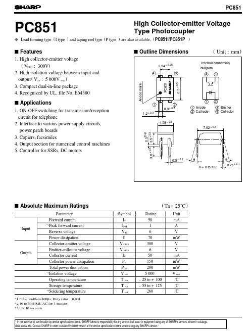
PC851
PC851
s Features
1. High collector-emitter voltage ( VCEO : 300V) 2. High isolation voltage between input and output ( Viso : 5 000V rms ) 3. Compact dual-in-line package 4. Recognized by UL, file No. E64380
( Unit : mm )
Internal connection
Anode mark
s Applications
1. ON-OFF switching for transmission/reception circuit for telephone 2. Interface to various power supply circuits, power patch boards 3. Copiers, facsimiles 4. Output section for numerical control machines 5. Controller for SSRs, DC motors
MB85RC16V(5V%2016KBit)

FUJITSU SEMICONDUCTORDATA SHEETCopyright©2011 FUJITSU SEMICONDUCTOR LIMITED All rights reserved 2011.8Memory FRAM16 K (2 K × 8) Bit I 2CMB85RC16V■DESCRIPTIONThe MB85RC16V is an FRAM (F erroelectric Random Access Memory) chip in a configuration of 2,048 words × 8 bits, using the ferroelectric process and silicon gate CMOS process technologies for forming the nonvolatile memory cells.Unlike SRAM, the MB85RC16V is able to retain data without using a data backup battery.The memory cells used in the MB85RC16V have at least 1010 Read/Write operation endurance per bit, which is a significant improvement over the number of read and write operations supported by other nonvolatile memory products.The MB85RC16V can provide writing in one byte units because the long writing time is not required unlike Flash memory and E 2PROM. Therefore, the writing completion waiting sequence like a write busy state is not required.■FEATURES•Bit configuration : 2,048 words × 8 bits •Operating power supply voltage : 3.0 V to 5.5 V •Operating frequency : 400 kHz (Max) •T wo-wire serial interface : Fully controllable by two ports: serial clock (SCL) and serial data (SDA).•Operating temperature range : − 40 °C to + 85 °C •Data retention : 10 years ( + 75 °C) •Read/Write endurance : 1010 times •Package : Plastic / SOP , 8-pin (FPT -8P-M02)•Low power consumption : Operating current 80 μA (Max: @400 kHz), Standby current 5 μA (Typ)DS501-00010-0v01-EMB85RC16V■PIN FUNCTIONAL DESCRIPTIONSPinNumberPin Name Functional Description1 to 3NC No Connect pins Leave it unconnected.4VSS Ground pin5SDA Serial Data I/O pinThis is an I/O pin of serial data for performing bidirectional communication of mem-ory address and writing or reading data. It is possible to connect some devices. It is an open drain output, so a pull-up resistance is required to be connected to the external circuit.6SCL Serial Clock pinThis is a clock input pin for input/output timing serial data. Data is sampled on the rising edge of the clock and output on the falling edge.7WP Write Protect pinWhen Write Protect pin is “H” level, writing operation is disabled. When Write Pro-tect pin is “L” level, the entire memory region can be overwritten. Reading operation is always enabled regardless of the Write Protect pin state. The write protect pin is internally pulled down to the VSS pin and that is recognized as the “L” level (write enabled) when the pin is the open state.8VDD Supply Voltage pinMB85RC16V■I2C (Inter-Integrated Circuit)The MB85RC16V has the two-wire serial interface and the I2C bus, and operates as a slave device.The I2C bus defines communication roles of “master” and “slave” devices, with the master side holding the authority to initiate control. Furthermore, a I2C bus connection is possible where a single master device is connected to multiple slave devices in a party-line configuration.2MB85RC16V■I2C COMMUNICATION PROTOCOLThe I2C bus provides communication by two wires only, therefore, the SDA input should change while SCL is the “L” level. However, when starting and stopping the communication sequence, SDA is allowed to change while SCL is the “H” level.•Start ConditionTo start read or write operations by the I2C bus, change the SDA input from the “H” level to the “L” level while the SCL input is in the “H” level.•Stop ConditionTo stop the I2C bus communication, change the SDA input from the “L” level to the “H” level while the SCL input is in the “H” level. In the reading operation, inputting the stop condition finishes reading and enters the standby state. In the writing operation, inputting the stop condition finishes inputting the rewrite data and enters the standby state.Note : The FRAM device does not need the programming wait time (t WC) after issuing the Stop Condition during the write operation.MB85RC16V ■ACKNOWLEDGE (ACK)In the I2C bus, serial data including memory address or memory information is sent in units of 8 bits. The acknowledge signal indicates that every 8 bits of the data is successfully sent and received. The receiver side usually outputs the “L” level every time on the 9th SCL clock after every 8 bits are successfully trans-mitted. On the transmitter side, the bus is temporarily released on this 9th clock to allow the acknowledge signal to be received and checked. During this released period, the receiver side pulls the SDA line down to indicate that the communication works correctly.If the receiver side receives the stop condition before transmitting the acknowledge “L” level, the read operation ends and the I2C bus enters the standby state. If the acknowledge “L” level is not detected, and the Stop condition is not sent, the bus remains in the released state without doing anything.■MEMORY ADDRESS STRUCTUREThe MB85RC16V has the memory address buffer to store the 11-bit information for the memory address.As for byte write, page write and random read commands, the complete 11-bit memory address is configured by inputting the memory upper address (3 bits) and the memory lower address (8 bits), and saving to the memory address buffer and access to the memory is performed.As for a current address read command, the complete 11-bit memory address is configured by inputting the memory upper address (3 bits) and by the memory address lower 8-bit which has saved in the memory address buffer, and saving to the memory address buffer and access to the memory is performed.MB85RC16V■DEVICE ADDRESS WORDF ollowing the start condition, the 8 bit device address word is input. Inputting the device address word decideswhether the master or the slave drives the data line. However, the clock is always driven by the master. The device address word (8bits) consists of a device T ype code (4bits), memory upper address code (3bits), anda Read/Write code (1bit).•Device Type Code (4bits)The upper 4 bits of the device address word are a device type code that identifies the device type, and are fixed at “1010” for the MB85RC16V.•Memory Upper Address Code (3bits)Following the device type code, the 3 bits of the memory upper address code are input.The slave address selection is not performed by the external pin setting on this device. These 3 bits are not the setting bits for the slave address, but the upper 3-bit setting bits for the memory address.•Read/Write Code (1bit)The 8th bit of the device address word is the R/W (Read/Write) code. When the R/W code is “0” input, a write operation is enabled, and the R/W code is “1” input, a read operation is enabled for the MB85RC16V.If the device code is not “1010”, the Read/Write operation is not performed and the standby state is chosen.MB85RC16V ■DATA STRUCTUREThe master inputs the device address word (8 bits) following the start condition, and then the slave outputs the Acknowledge “L” level on the ninth bit. After confirming the Acknowledge response, the sequential 8-bit memory lower address is input, to the byte write, page write and random read commands.As for the current address read command, inputting the memory lower address is not performed, and the address buffer lower 8-bit is used as the memory lower address.When inputting the memory lower address finishes, the slave outputs the Acknowledge “L” level on the ninth bit again.Afterwards, the input and the output data continue in 8-bit units, and then the Acknowledge “L” level is output for every 8-bit data.MB85RC16V■FRAM ACKNOWLEDGE -- POLLING NOT REQUIREDThe MB85RC16V performs the high speed write operations, so any waiting time for an ACK* by the acknowl-edge polling does not occur.*: In Flash memory and E2PROM, the Acknowledge Polling is performed as a progress check whether rewriting is executed or not. It is normal to judge by the 9th bit of Acknowledge whether rewriting is performed or not after inputting the start condition and then the device address word (8 bits) during rewriting.■WRITE PROTECT (WP)The entire memory array can be write protected by setting the WP pin to the “H” level. When the WP pin is set to the “L” level, the entire memory array will be rewritten. Reading is allowed regardless of the WP pin's “H” level or “L” level.Do not change the WP signal level during the communication period from the start condition to the stop condition.Note : The WP pin is pulled down internally to the VSS pin, therefore if the WP pin is open, the pin status is recognized as the “L” level (write enabled).MB85RC16V ■COMMAND•Byte WriteIf the device address word (R/W “0” input) is sent after the start condition, an ACK responds from the slave.After this ACK, write memory addresses and write data are sent in the same way, and the write ends by•Page WriteIf data is continuously sent after the following address when the same command (expect stop condition) as Byte Write was sent, a page write is performed. The memory address rolls over to first memory address (000H)at the end of the address. Therefore, if more than 2 Kbytes are sent, the data is overwritten in orderMB85RC16V•Current Address ReadIf the last write or read operation finishes correctly up to the end of stop condition, the memory address that was accessed last remains in the memory address buffer (the length is 11 bits).When sending this command without turning the power off, it is possible to read from the memory address n+1 which adds 1 to the total 11-bit memory address n, which consists of the memory upper address 3-bit from the device address word input and the lower 8-bit of the memory address buffer. If the memory address n is the last address, it is possible to read with rolling over to the head of the memory address (000H). The current address (address that the memory address buffer indicates) is undefined immediately after turning•Random ReadAfter specifying the address as well as for write system command, issuing another start condition, by trans-mitting Device Address Word (R/W “1” input), the one byte data from the memory address saved in the memory address buffer can be read synchronously to SCL.Setting values for the first and the second memory upper address codes should be the same (The figure below shows the input example).The final NACK (SDA is the “H” level) is issued by the receiver that receives the data. In this case, this bit is•Sequential ReadData can be received continuously following the Device address word (R/W “1” input) after specifying the address in the same way as for Random Read. If the read reaches the end of address, the read address■ABSOLUTE MAXIMUM RATINGS*: These parameters are based on the condition that Vss is 0 V .WARNING:Semiconductor devices can be permanently damaged by application of stress (voltage, current,temperature, etc.) in excess of absolute maximum ratings. Do not exceed these ratings.■RECOMMENDED OPERATING CONDITIONS*: These parameters are based on the condition that Vss is 0 V .WARNING:The recommended operating conditions are required in order to ensure the normal operation ofthe semiconductor device. All of the device's electrical characteristics are warranted when the device is operated within these ranges.Always use semiconductor devices within their recommended operating condition ranges.Operation outside these ranges may adversely affect reliability and could result in device failure.No warranty is made with respect to uses, operating conditions, or combinations not represented on the data sheet. Users considering application outside the listed conditions are advised to contact their representatives beforehand.ParameterSymbol RatingUnit Min Max Power supply voltage*V DD − 0.5 + 6.0V Input voltage*V IN − 0.5V DD + 0.5 ( ≤ 6.0)V Output voltage*V OUT − 0.5V DD + 0.5 ( ≤ 6.0)V Ambient temperature T A − 40 + 85 °C Storage temperatureT STG− 40+ 125°CParameterSymbol ValueUnit Min Typ Max Power supply voltage*V DD 3.0⎯ 5.5V “H” level input voltage*V IH V DD × 0.8⎯ 5.5V “L” level input voltage*V IL V SS ⎯V DD × 0.2V Ambient temperatureT A− 40⎯+ 85°C■ELECTRICAL CHARACTERISTICS1.DC Characteristics(within recommended operating conditions)*1: Applicable pin: SCL,SDA *2: Applicable pin: SDAParameterSymbol ConditionValueUnit Min Typ Max Input leakage current*1|I LI |V IN = 0 V to V DD ⎯⎯1μA Output leakage current*2|I LO |V OUT = 0 V to V DD ⎯⎯1μA Operating power supply current I CC SCL = 400 kHz⎯4080μA Standby current I SB SCL, SDA = V DDWP = 0V or V DD or OPEN T A = + 25 °C in stop condi-tion⎯510μA “L” level output voltage V OL I OL = 2 mA ⎯⎯0.4V Input resistance for WP pin R INV IN = V IL (Max)50⎯⎯k ΩV IN = V IH (Min)1⎯⎯M Ω2.AC Characteristics(within recommended operating conditions)AC characteristics were measured under the following measurement conditions.Power supply voltage : 3.0 V to 5.5 V Operating temperature : − 40 °C to + 85 °C Input voltage amplitude : V DD × 0.2 to V DD × 0.8 Input rise time : 5 ns Input fall time : 5 ns Input judge level : V DD /2 Output judge level: V DD /2ParameterSymbolValueUnitSTANDARD MODE FAST MODE MinMax Min Max SCL clock frequency FSCL 01000400kHz Clock high time T HIGH 4.0⎯0.6⎯μs Clock low time T LOW 4.7⎯ 1.3⎯μs SCL/SDA rise time T r ⎯1000⎯300ns SCL/SDA fall time T f ⎯300⎯300ns Start condition hold T HD:STA 4.0⎯0.6⎯μs Start condition setup T SU:STA 4.7⎯0.6⎯μs SDA input hold T HD:DAT 0⎯0⎯ns SDA input setup T SU:DAT 250⎯100⎯ns SDA output hold T DH:DAT 0⎯0⎯ns Stop condition setupT SU:STO 4.0⎯0.6⎯μs SDA output access after SCL fall T AA ⎯3⎯0.9μs Pre-charge timeT BUF 4.7⎯ 1.3⎯μs Noise suppression time constant on SCL, SDAT SP⎯50⎯50ns4.Pin capacitanceParameter Symbol Conditions ValueUnit Min Typ Max I/O capacitance C I/O V DD = V IN = V OUT = 0V, f = 1 MHz, T A = + 25 °C⎯⎯15pF Input capacitanceC IN⎯⎯15pF■NOTES ON USE•Data written before performing IR reflow is not guaranteed after IR reflow.•VDD is required to be rising from 0 V because turning the power on from an intermediate level may cause malfunctions, when the power is turned on.ParameterSymbol ValueUnit Min Max SDA, SCL level hold time during power down tpd 85⎯ ns SDA, SCL level hold time during power up tpu 85⎯ ns Power supply rise time tr 0.550ms Power supply fall time tf 0.0150ms Power off timetOFF50⎯ms■ORDERING INFORMATIONPart number Package RemarksMB85RC16VPNF-G-JNE1 8-pin, plastic SOP (FPT-8P-M02)MB85RC16VPNF-G-JNERE1 8-pin, plastic SOP(FPT-8P-M02)Embossed Carrier tape■PACKAGE DIMENSIONPlease check the latest package dimension at the following URL. /package/en-search/MEMOFUJITSU SEMICONDUCTOR LIMITED Nomura Fudosan Shin-yokohama Bldg. 10-23, Shin-yokohama 2-Chome, Kohoku-ku Y okohama Kanagawa 222-0033, JapanT el: +81-45-415-5858/fsl/en/For further information please contact:North and South AmericaFUJITSU SEMICONDUCTOR AMERICA, INC. 1250 E. Arques Avenue, M/S 333Sunnyvale, CA 94085-5401, U.S.A.T el: +1-408-737-5600 Fax: +1-408-737-5999 /micro/EuropeFUJITSU SEMICONDUCTOR EUROPE GmbH Pittlerstrasse 47, 63225 Langen, GermanyT el: +49-6103-690-0 Fax: +49-6103-690-122 /semiconductor/KoreaFUJITSU SEMICONDUCTOR KOREA LTD.902 Kosmo T ower Building, 1002 Daechi-Dong, Gangnam-Gu, Seoul 135-280, Republic of Korea T el: +82-2-3484-7100 Fax: +82-2-3484-7111 /fsk/Asia PacificFUJITSU SEMICONDUCTOR ASIA PTE. LTD.151 Lorong Chuan,#05-08 New T ech Park 556741 SingaporeT el : +65-6281-0770 Fax : +65-6281-0220/semiconductor/FUJITSU SEMICONDUCTOR SHANGHAI CO., LTD. Rm. 3102, Bund Center, No.222 Y an An Road (E), Shanghai 200002, ChinaT el : +86-21-6146-3688 Fax : +86-21-6335-1605 /fss/FUJITSU SEMICONDUCTOR P ACIFIC ASIA LTD. 10/F., World Commerce Centre, 11 Canton Road, Tsimshatsui, Kowloon, Hong KongT el : +852-2377-0226 Fax : +852-2376-3269/fsp/Specifications are subject to change without notice. For further information please contact each office.All Rights Reserved.The contents of this document are subject to change without notice.Customers are advised to consult with sales representatives before ordering.The information, such as descriptions of function and application circuit examples, in this document are presented solely for the purpose of reference to show examples of operations and uses of FUJITSU SEMICONDUCTOR device; FUJITSU SEMICONDUCTOR does not warrant proper operation of the device with respect to use based on such information. When you develop equipment incorporating the device based on such information, you must assume any responsibility arising out of such use of the information.FUJITSU SEMICONDUCTOR assumes no liability for any damages whatsoever arising out of the use of the information.Any information in this document, including descriptions of function and schematic diagrams, shall not be construed as license of the use or exercise of any intellectual property right, such as patent right or copyright, or any other right of FUJITSU SEMICONDUCTOR or any third party or does FUJITSU SEMICONDUCTOR warrant non-infringement of any third-party's intellectual property right or other right by using such information. FUJITSU SEMICONDUCTOR assumes no liability for any infringement of the intellectual property rights or other rights of third parties which would result from the use of information contained herein.The products described in this document are designed, developed and manufactured as contemplated for general use, including without limitation, ordinary industrial use, general office use, personal use, and household use, but are not designed, developed and manufactured as contemplated (1) for use accompanying fatal risks or dangers that, unless extremely high safety is secured, could have a serious effect to the public, and could lead directly to death, personal injury, severe physical damage or other loss (i.e., nuclear reaction control in nuclear facility, aircraft flight control, air traffic control, mass transport control, medical life support system, missile launch control in weapon system), or (2) for use requiring extremely high reliability (i.e., submersible repeater and artificial satellite).Please note that FUJITSU SEMICONDUCTOR will not be liable against you and/or any third party for any claims or damages aris-ing in connection with above-mentioned uses of the products.Any semiconductor devices have an inherent chance of failure. You must protect against injury, damage or loss from such failures by incorporating safety design measures into your facility and equipment such as redundancy, fire protection, and prevention of over-current levels and other abnormal operating conditions.Exportation/release of any products described in this document may require necessary procedures in accordance with the regulations of the Foreign Exchange and Foreign Trade Control Law of Japan and/or US export control laws.The company names and brand names herein are the trademarks or registered trademarks of their respective owners.Edited: Sales Promotion Department。