LTC2309CUF#PBF;LTC2309IUF#PBF;LTC2309HF#PBF;LTC2309CUF#TRPBF;LTC2309CF#PBF;中文规格书,Datasheet资料
LTC2941 LTC2942 电池气体计测试电路说明书

DC1496A-A1dc1496fD ESCRIPTION Battery Gas Gauge with I 2C Interface [and 14-Bit ADC(DC1496A-B)]Demonstration circuit 1496A-A (Figure 1) features the L TC ®2941. Demonstration circuit 1496A-B features the L TC2942. Both devices measure battery charge state in handheld PC and portable product applications. The operating range is perfectly suited for single cell Li-Ion batteries. A precision analog coulomb counter integrates current through a sense resistor between the battery’s positive terminal and the load or charger . The L TC2942 adds battery voltage and on-chip temperature measurement with an internal 14-bit No Latency ΔΣ™ ADC. The three measured quantities (charge, voltage and temperature) are stored in internal registers accessible via the onboard SMBus/I 2C interface.The L TC2941 has programmable high and low thresholds for accumulated charge. The L TC2942 has programmable high and low thresholds for all three measured quantities. If a programmed threshold is exceeded, the device reports an alert using either the SMBus alert protocol or by setting a fl ag in the internal status register .L , L T , L TC, L TM, Linear Technology and the Linear logo are registered trademarks and No Latency ΔΣ is a trademark of Linear Technology Corporation. All other trademarks are the property of their respective owners.The L TC2941 and L TC2942 require only a single low value sense resistor to set the measured current range. The default value assembled on the DC1496 is 100mΩ for a maximum current measurement of 500mA. Both parts have a software-confi gurable charge complete/alert pin. When the pin is set for charge complete, a jumper con-nects the pushbutton which simulates a logic high input to indicate a full battery. When the pin is confi gured for alert, the same jumper is used to connect a red LED that indicates an alert is present.The DC1496A-A/B is a part of the QuikEval system for quick evaluation with a host controller through a PC.Design fi les for this circuit board are available at http://www.linear.com/demo.Figure 1. DC1496A-A/B2dc1496fDEMO MANUAL DC1496A-A/B QUICK START PROCEDUREDemonstration circuit 1496A is easy to set up to evaluate the performance of the L TC2941/L TC2942. Refer to Figure 2 for proper measurement equipment setup and follow the procedure below.1. C onnect a 1-cell Li-I on battery across V_BAT and GND.2. Connect a load across V_CHRG/LD and GND for battery discharge measurement. Up to 500mA supplied from the battery can be measured with the board default 100mΩ sense resistor . Use SENSE + and SENSE – test points to read voltage across the sense resistor .3. Connect a 2.7V to 5.5V battery charger supply across V_CHRG/LD and GND. Up to 500mA supplied to the battery can be measured with the board default 100mΩ sense resistor . Use SENSE + and SENSE – test points to read voltage across the sense resistor .4. Connect a DC590 to 14-pin connector J1 for evaluation with QuikEval, or connect a host controller I 2C bus to the SDA, SCL and GND test turrets.5. Set JP1 to QuikEval if a DC590 is present. Otherwise set JP1 to Bat/Chrg for bus pull-up to the battery, or fl oat JP1 and supply a bus pull-up voltage to VP .6. Read and write to the L TC2941/L TC2942 through I 2C.7. Through I 2C, configure the AL /CC pin. Set JP2 accordingly.8 f AL /CC is set for charge complete, use pushbutton switch S1 to simulate a logic high from a controller to indicate a fully charged battery.Figure 2. DC1496A-A/B Basic Setup3dc1496fDEMO MANUAL DC1496A-A/BQuikEval INTERFACEThe DC1496A-A/B can be connected to a DC590 and used with the QuikEval software. The DC590 connects to a PC through USB. QuikEval automatically detects the demo board and brings up the L TC2941/L TC2942 evaluation software interface (Figure 3). Compact and Detailed FormWhen the interface is brought up, a compact form is fi rst shown with a display for the accumulated charge register (ACR), voltage ADC and temperature ADC. To expand the form for a more detailed display of the L TC2941/L TC2942 registers and board confi gurations, click on Detail. To go back to the compact form, click on Hide.Start/RefreshClick on Start to begin a polling routine that refreshes the interface every 1 second. Click on Stop to halt the poll-ing. For a single update, click on Refresh. Each refresh scans through the internal I 2C registers and updates the respective displays.L TC2941 and L TC2942 DisplayOn a refresh or poll, the software reads Status bit A[7] to determine communication with an L TC2941 or L TC2942. When an L TC2941 is detected, the voltage and temperature ADC and threshold displays are not shown. Control bits B[7:6] confi gure VBAT Alert for the L TC2941 and ADC Mode for the L TC2942.ACR DisplayThe data in the ACR (registers C and D) is displayed in one of three selected formats: Counter in coulombs, Counter in mA • hour , battery gas gauge in mA • hour , and battery gas gauge in charge percentage of battery. The two gas gauge displays correspond to the battery gas gauge full battery confi guration set in the detailed form.Voltage and Temperature ADC (L TC2942)Data from the Voltage ADC (registers I and J) and the Temperature ADC (registers M and N) is displayed here in Volts and Celsius.Figure 3. L TC2941/LTC2942 QuikEval InterfaceDEMO MANUAL DC1496A-A/B QuikEval INTERFACEAddress/I2C StatusThe write address for the L TC2941/L TC2942 is C8h and the read address is C9h. The alert response address (ARA) is 19h. If an error occurs while reading from the L TC2941/ L TC2942, the I2C status will read as an error. Otherwise, the status is good. If the L TC2941/L TC2942 AL/CC pin is set for alert mode and an alert has been latched, the device will pull down this pin. Click on ARA to send out an ARA on to the bus lines and the device will respond with its address. The Alert pin will then be cleared if the alert is no longer present.StatusThe individual status bits A[0:7] and their states are shown here. A red indicator next to bits A[0:5] indicates the re-spective alert is currently present and will latch the Alert pin if confi gured for alert. Bit A[7] shows if an L TC2941 or L TC2942 is detected.Sense ResistorEnter here the sense resistor value used in the application. The default for the DC1496A-A/B is a 100mΩ sense resis-tor. Check L TC2941-1/L TC2942-1 if one of these devices is used in place of the default IC. This sets the sense resistor value to 50mΩ, the value of the internal sense resistor in these devices. The sense resistor can only be changed when not polling. The software only accepts sense resis-tors between 0.1mΩ to 5Ω.Battery Gas GaugeThe battery capacity in the application is entered here. The ACR full scale (FFFFh) is set to this value and affects the two Gas Gauge ACR display options. Instead of counting up from 0 as in the Coulomb Counters, the Gas Gauge is used to count down from a full battery. The battery capacity can only be entered when not polling. The data in the ACR when a battery should be empty is calculated based off of R SENSE, and pre-scaler M, and displayed in hexadecimal below the ACR full scale.ControlConfi gurations done in the Control section write to the Control register (register B). For the L TC2941, the Control bits B[7:6] enables a battery monitor to one of three set voltage thresholds (2.8V, 2.9V, or 3V) or disables this battery voltage alert. The ADC mode with the L TC2942 is default to Sleep where both Voltage and Temperature ADCs (L TC2942) are disabled. Setting ADC Mode to Automatic Mode enables full-time the Voltage and Temperature ADC. Selecting Manual Voltage or Temperature mode enables the respective ADC once and returns the ADC to Sleep mode.Select a pre-scaler M value to scale the ACR according to battery capacity and maximum current. Changing the pre-scaler will halt the poll. A calculator tool is provided in the tool bar under Tools to assist in calculating a pre-scaler value and sense resistor (Figure 4).The AL#/CC pin can be confi gured for Alert mode, Charge Complete mode, or disabled. Select the corresponding settings on the DC1496A-A/B jumper J2.The Shutdown Analog Section is checked to disable the Analog portion of the L TC2941/42 and set the device in a low current state.Register Read/WriteData in the internal registers of the L TC2941/L TC2942 is displayed here in hexadecimal or appropriate units. Data can also be entered and written to the write registers. Enter data to be written in hexadecimal, or select Unit and enter data in decimal form. Data in decimal scale is auto corrected if the maximum or minimum full scale is exceeded. Select the ACR display in Counter (Coulombs) to be able to write to the ACR and charge thresholds in Coulombs, or select Counter (mAh) to be able to write to the ACR and charge thresholds in mA • hour. Voltage and Temperature High thresholds are rounded down in the calculations to the nearest lower count, while the low thresholds are rounded up to nearest higher count.4dc1496f5dc1496fDEMO MANUAL DC1496A-A/BSwitching back and forth between Hex and Unit can be used as a conversion tool.The LSB value for the 16-bit ACR and charge thresholds is displayed on the bottom. This value is adjusted with the sense resistor and pre-scaler M. The units are in mAh or mC depending on the selected ACR display. Shown for the L TC2942 is the LSB for the 14-bit voltage ADC, 10-bit temperature ADC, and 8-bit high and low thresholds for voltage and temperature.Calculator ToolA calculator tool is available in the tool bar options under Tools. In this calculator (Figure 4), enter the maximum cur-rent passed through the sense and the maximum battery capacity. Click on Calculate to calculate a recommended sense resistor and pre-scaler (M) value. The display shows the battery capacity in comparison to ACR full scale and provides an LSB value in mAh. Also shown is the recom-mended equation to use to determine an appropriate sense resistor as a function of the maximum battery charge and maximum current.Figure 4. L TC2941/L TC2942 Pre-Scaler and Sense Resistor CalculatorQuikEval INTERFACEDEMO MANUAL DC1496A-A/BPARTS LISTITEM QTY REFERENCE PART DESCRIPTION MANUFACTURE/PART NUMBER12C1, C2CAP., CHIP X7R, 0.1μF, 25V, 0603AVX, 06033C104KAT2A24E1-E4TURRET, Test Point 0.094"MILL-MAX, 2501-2-00-80-00-00-07-035E5-E9TURRET, Test Point 0.064"MILL-MAX, 2308-241E10, E11TURRET, Test Point 0.037"MILL-MAX, 2309-150TP1, TP2(SMT Pads Only)62JP1, JP2HEADER, 3Pin 1 Row 0.079CC SAMTEC, TMM-103-02-L-S72for (JP1, JP2)SHUNT, 0.079" Center SAMTEC, 2SN-BK-G81J1HEADERS, Vertical Dual 2X7 0.079CC MOLEX, 87831-142091D1LED, RED, LIGHT EMITTING DIODES PANASONIC, LN1251CTR101R1RES., CHIP, 0.1Ω, 1/8W, 1%, 1206IRC, LRC-LR1206LF-01-R100-F113R6, R7, R8RES., CHIP, 5.10k, 1%, 0603VISHAY, CRCW06035K10FKEA123R2, R3, R4RES., CHIP, 10k, 5%, 0603VISHAY, CRCW060310K0JNEA131R5RES., CHIP, 1k, 5%, 0603VISHAY, CRCW06031K00JNEA141R9RES., CHIP, 100k, 5%, 0603VISHAY, CRCW0603100KJNEA151S1SWITCH, SMT Pushbutton PANASONIC, EVQPE105K161U2I.C., Serial EEPROM TSSOP8MICROCHIP, 24LC025-I/ST171for (J1)CABLE ASSY., 8" STRIP LINEAR RIBBON CABLE CA-24406dc1496f7dc1496fDEMO MANUAL DC1496A-A/BSCHEMATIC DIAGRAM8dc1496fDEMO MANUAL DC1496A-A/B Silkscreen TopComponent SideInner Layer 2PCB LAYOUT AND FILM9dc1496fDEMO MANUAL DC1496A-A/BI nformation furnished by Linear Technology Corporation is believed to be accurate and reliable. However , no responsibility is assumed for its use. Linear Technology Corporation makes no representation that the interconnection of its circuits as described herein will not infringe on existing patent rights.PCB LAYOUT AND FILMInner Layer 3Solder SideSilkScreen Bottom10dc1496f DEMO MANUAL DC1496A-A/BLinear Technology Corporation 1630 McCarthy Blvd., Milpitas, CA 95035-7417(408) 432-1900 ● FAX: (408) 434-0507 ● www.linear .com © LINEAR TECHNOLOGY CORPORA TION 2010LT 0510 • PRINTED IN USADEMONSTRATION BOARD IMPORTANT NOTICELinear Technology Corporation (L TC) provides the enclosed product(s) under the following AS IS conditions:This demonstration board (DEMO BOARD) kit being sold or provided by Linear Technology is intended for use for ENGINEERING DEVELOPMENT OR EVALUATION PURPOSES ONL Y and is not provided by L TC for commercial use. As such, the DEMO BOARD herein may not be complete in terms of required design-, marketing-, and/or manufacturing-related protective considerations, including but not limited to product safety measures typically found in finished commercial goods. As a prototype, this product does not fall within the scope of the European Union direc-tive on electromagnetic compatibility and therefore may or may not meet the technical requirements of the directive, or other regulations.If this evaluation kit does not meet the specifications recited in the DEMO BOARD manual the kit may be returned within 30 days from the date of delivery for a full refund. THE FOREGOING WARRANTY IS THE EXCLUSIVE WARRANTY MADE BY THE SELLER TO BUYER AND IS IN LIEU OF ALL OTHER WARRANTIES, EXPRESSED, IMPLIED, OR STATUTORY, INCLUDING ANY WARRANTY OF MERCHANTABILITY OR FITNESS FOR ANY PARTICULAR PURPOSE. EXCEPT TO THE EXTENT OF THIS INDEMNITY, NEITHER PARTY SHALL BE LIABLE TO THE OTHER FOR ANY INDIRECT , SPECIAL, INCIDENTAL, OR CONSEQUENTIAL DAMAGES.The user assumes all responsibility and liability for proper and safe handling of the goods. Further , the user releases L TC from all claims arising from the handling or use of the goods. Due to the open construction of the product, it is the user’s responsibility to take any and all appropriate precautions with regard to electrostatic discharge. Also be aware that the products herein may not be regulatory compliant or agency certified (FCC, UL, CE, etc.).No License is granted under any patent right or other intellectual property whatsoever. L TC assumes no liability for applications assistance, customer product design, software performance, or infringement of patents or any other intellectual property rights of any kind.L TC currently services a variety of customers for products around the world, and therefore this transaction is not exclusive .Please read the DEMO BOARD manual prior to handling the product . Persons handling this product must have electronics training and observe good laboratory practice standards. Common sense is encouraged .This notice contains important safety information about temperatures and voltages. For further safety concerns, please contact a L TC applica-tion engineer .Mailing Address:Linear Technology1630 McCarthy Blvd.Milpitas, CA 95035Copyright © 2004, Linear Technology CorporationDC1496A-A。
LTC2309中文资料
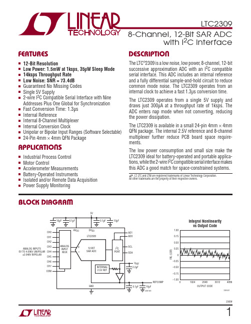
12-Bit Resolution Low Power: 1.5mW at 1ksps, 35μW Sleep Mode 14ksps Throughput Rate Low Noise: SNR = 73.4dB Guaranteed No Missing Codes Single 5V Supply 2-wire I2C Compatible Serial Interface with Nine Addresses Plus One Global for Synchronization Fast Conversion Time: 1.3μs Internal Reference Internal 8-Channel Multiplexer Internal Conversion Clock Unipolar or Bipolar Input Ranges (Software Selectable) 24-Pin 4mm × 4mm QFN Package
l
The l denotes the specifications which apply over the full operating temperature range, otherwise specifications are at TA = 25°C. (Notes 4, 5)
MIN 12 TYP ±0.45 ±0.35 ±1 0.002 ±0.1 ±0.4 0.002 ±0.2 ±0.5 ±0.4 0.05 ±0.4 ±0.4 ±0.3 0.05 ±0.3 MAX ±1 ±1 ±8 ±3 ±6 ±1 ±10 ±9 ±3 ±10 ±6 ±2 UNITS Bits LSB LSB LSB LSB/°C LSB LSB LSB/°C LSB LSB LSB LSB/°C LSB LSB LSB LSB/°C LSB
LTC4306IUFD-DC906A-用户手册说明书

QUICK START GUIDE FOR DEMONSTRATION CIRCUIT 906A4-CHANNEL, 2-WIRE BUS MULTIPLEXER WITH CAPACITANCE BUFFERINGLTC4306IUFDDESCRIPTIONDemonstration circuit 906A features the LTC ®4306IUFD, a 4-channel, 2-wire I2C bus and SMBus compatible multiplexer having bus buffers that provide capacitive isolation between the up-stream bus and downstream buses. Through soft-ware control, the LTC4306IUFD connects the up-stream 2-wire bus to any desired combination of downstream buses. Each bus can be pulled up to a supply voltage ranging from 2.2V to 5.5V, independ-ent of the LTC4306IUFD supply voltage. The down-stream buses are also provided with ALERT1B – ALERT4B inputs for fault reporting.Programmable timeout circuitry disconnects the downstream buses if the bus is stuck low. When acti-vated, rise time accelerators source currents into the 2-wire bus pins during rising edges to reduce rise time. Two general purpose input/output (GPIO) pins can be configured as inputs, open-drain outputs or push-pull outputs. Green LED’s D3 and D2 light up when GPIO1 and GPIO2, respectively, are low. Driv-ing the ENABLE pin low restores all device features totheir default states. Three address pins provide 27 distinct addresses.Design files for this circuit board are available. Call the LTC factory.LTC is a registered trademark of Linear Technology CorporationTable 1. Performance Summary (T A = 25°C)PARAMETERCONDITION VALUE V CC Voltage Operating Range2.7V – 5.5V Bus Pull-up Supply Voltage Range (V BUS1-V BUS4) 2.2V – 5.5V 2-Wire Bus Frequency Range0 - 400kHzBus Stuck Low Disconnect TimesV CC = 2.7V - 5.5V7.5ms, 15ms, 30ms optionsall times +/-16.7% feature can also be disabledBus Buffer V OL Offset Voltage R BUS = 10K 100mV (maximum) V CC = 3.3V 5.5mA (typical) Rise Time Accelerator Pull-up Current V CC = 5V9mA (typical) ALERTB and READY Output V OL VoltagesV CC = 2.7V - 5.5V; I ALERTB = I READY = 3mA0.4V (maximum)OPERATING PRINCIPLESFor operation with the DC906A, connect the host con-troller’s SDA and SCL pins to the LTC4306IUFD’s SDAIN and SCLIN pins (hereafter referred to as the upstream bus), and connect the upstream bus supply of 2.7V to 5.5V to Vcc (as shown in Figure 1). The host controller on the upstream side first addresses and configures the LTC4306IUFD to connect the up-stream bus to one or more of the four downstreambuses. Communications between the upstream and downstream components are then established and a host controller on any bus can then control the LTC4306IUFD.Use turrets VBUS1-VBUS4 and jumpers JP1-JP4 to pull up the downstream buses to supply voltages dif-ferent than VCC (i.e., to provide level-shifting). Forexample, in Figure1, JP1 is set to the right position and a supply voltage is connected between VBUS1 and ground. Voltages on VBUS1-VBUS4 must range between 2.2V and 5.5V. To connect a downstream bus’s pull-up supply to VCC, set its jumper to the left position.Additional configurations include enabling and dis-abling the rise time accelerators on the backplane side and/or the card side, setting the GPIO’s to open-drain output, push-pull output, or input mode, setting or resetting the GPIO’s outputs, disabling the Bus Stuck Low disconnect feature or setting the discon-nect time to 7.5ms, 15ms, 30ms. A host controller can also read the internal registers of the LTC4306IUFD to determine the settings of these fea-tures as well as fault statuses. All of these features are accessed by sending commands on the 2-wire bus.The ENABLE pin, when pulled low, resets the LTC4306IUFD to its registers default state and dis-ables communication to it. Communication can be reestablished when ENABLE is released high. There-fore, set jumper JP5 to the left position for normal operation, and set it to the right position to disable the LTC4306IUFD.Slave devices that are capable of fault reporting and that are located on downstream buses 1-4 should connect their fault pins to ALERT1B-ALERT4B, re-spectively. The LTC4306IUFD passes downstream faults to the upstream host by pulling down on the ALERTB pin, so this host’s fault input should be con-nected to the LTC4306IUFD ALERTB pin.When the upstream bus is connected to one or more downstream buses, the READY pin voltage is pulled up to VCC. When the upstream bus is disconnected from all downstream buses, the READY voltage is low (~0.2V).On the DC906A, the board’s default setting for jump-ers JP6, JP7 and JP8 is the center position, which sets the address of the LTC4306IUFD to (1001 010)2. To set a different address, configure the jumpers ac-cording to Table 1 of the data sheet (note: left posi-tion = H, middle position = NC, right position = L; de-fault = NC for all three jumpers).QUICK START PROCEDUREDemonstration circuit 906A is easy to set up to evalu-ate the performance of the LTC4306IUFD. Refer toFigure 1 for proper measurement equipment setup and follow the procedure below:KEY NOTES: a. Do not activate rise time acceleratorson buses whose pull-up supply voltages are lower than VCC. b. Make sure logic low voltages forced onall clock and data pins are < 0.4V. c. When activatingmultiple downstream buses that are powered from separate supply voltages, make sure that theLTC4306IUFD’s VCC voltage is less than or equal tothe lowest downstream bus pull-up supply voltage. 1.Jumpers JP1-JP4 choose the pull-up supply volt-ages VBUS1 – VBUS4 for downstream buses 1-4.For unused buses and buses pulled up to VCC, set the jumpers in the left position. To pull up a down-stream bus to a different voltage than VCC, set itsjumper to the right position, and connect the sup-ply voltage to the appropriate turret on the left side of the board.2.Set jumper J5 in the left position to enable communication to the LTC4306IUFD.3.Configure jumpers JP6 – JP8 to set the desired 2-wire bus address for the LTC4306IUFD according to Table 1 on page 13 of the datasheet (note: left position = H, middle position = NC, right position = L; default = NC for all three jumpers).4.Connect a cable from 6-pin header J2 to a board containing the master device(s).5.Connect a 20-pin ribbon cable from J1 to a board that contains downstream slave devices. Note: the downstream buses can contain masters, but the original command to connect must come from amaster connected to the upstream SDAIN/SCLIN bus.6. Connect power supplies to VCC and, if required,one or more of VBUS1 – VBUS4.7. Turn on the power supplies.NOTE: Make sure that the power supply voltages donot exceed 5.5V.8. Use the SMBus Read Byte and Write Byte proto-cols in conjunction with the register definitions on pages 8 and 9 of the datasheet to experiment with the LTC4306IUFD’s features and to establish up-stream-downstream communications between the master and slave devices.Figure 1.Proper Measurement Equipment Setup。
LTC4213 1 4213f 电子电路保护器说明书

2µs/DIV4213 TA01b124213fBias Supply Voltage (V CC )...........................–0.3V to 9V Input VoltagesON, SENSEP, SENSEN.............................–0.3V to 9V I SEL ..........................................–0.3V to (V CC + 0.3V)Output VoltagesGATE .....................................................–0.3V to 15V READY.....................................................–0.3V to 9V Operating Temperature RangeLTC4213C ...............................................0°C to 70°C LTC4213I.............................................–40°C to 85°C Storage Temperature Range.................–65°C to 150°C Lead Temperature (Soldering, 10sec)...................300°CORDER PART NUMBER DDB PART*MARKING T JMAX = 125°C, θJA = 250°C/WEXPOSED PAD (PIN 9)PCB CONNECTION OPTIONALConsult LTC Marketing for parts specified with wider operating temperature ranges.*The temperature grade is identified by a label on the shipping container.LBHVLTC4213CDDB LTC4213IDDB ABSOLUTE AXI U RATI GSW W WU PACKAGE/ORDER I FOR ATIOUUW (Note 1)ELECTRICAL CHARACTERISTICSThe ● denotes the specifications which apply over the full operatingtemperature range, otherwise specifications are at T A = 25°C. V CC = 5V, I SEL = 0 unless otherwise noted. (Note 2)SYMBOL PARAMETER CONDITIONSMIN TYP MAX UNITSV CC Bias Supply Voltage ● 2.36V V SENSEP SENSEP Voltage ●06V I CC V CC Supply Current●1.63mA V CC(UVLR)V CC Undervoltage Lockout Release V CC Rising● 1.8 2.07 2.23V ∆V CC(UVHYST)V CC Undervoltage Lockout Hysteresis ●30100160mV I SENSEP SENSEP Input Current V SENSEP = V SENSEN = 5V, Normal Mode 154080µA V SENSEP = V SENSEN = 0, Normal Mode –1±15µA I SENSENSENSEN Input CurrentV SENSEP = V SENSEN = 5V, Normal Mode 154080µA V SENSEP = V SENSEN = 0, Normal Mode –1±15µA V SENSEP = V SENSEN = 5V,50280µAReset Mode or Fault ModeV CBCircuit Breaker Trip Voltage I SEL = 0, V SENSEP = V CC●22.52527.5mV V CB = V SENSEP – V SENSEN I SEL = Floated, V SENSEP = V CC ●455055mV I SEL = V CC, V SENSEP = V CC ●90100110mV V CB(FAST)Fast Circuit Breaker Trip Voltage I SEL = 0, V SENSEP = V CC●63100115mV V CB(FAST)= V SENSEP – V SENSEN I SEL = Floated, V SENSEP = V CC ●126175200mV I SEL = V CC, V SENSEP = V CC ●252325371mV I GATE(UP)GATE Pin Pull Up Current V GATE = 0V●–50–100–150µA I GATE(DN)GATE Pin Pull Down Current ∆V SENSEP – V SENSEN = 200mV, V GATE = 8V ●1040mA ∆V GSMAX External N-Channel Gate Drive V SENSEN = 0, V CC ≥ 2.97V, I GATE = –1µA ● 4.8 6.58V V SENSEN = 0, V CC = 2.3V, I GATE = –1µA ● 2.65 4.38V ∆V GSARMV GS Voltage to Arm Circuit BreakerV SENSEN = 0, V CC ≥ 2.97V ● 4.4 5.47.6V V SENSEN = 0, V CC = 2.3V●2.53.57VTOP VIEWDDB PACKAGE8-LEAD (3mm × 2mm) PLASTIC DFN567894321READY ON I SEL GND V CC SENSEP SENSEN GATE34213f∆V GSMAX – ∆V GSARM Difference Between ∆V GSMAX and V SENSEN = 0, V CC ≥ 2.97V ●0.3 1.1V ∆V GSARMV SENSEN = 0, V CC = 2.3V●0.150.8VV READY(OL)READY Pin Output Low Voltage I READY = 1.6mA, Pull Down Device On ●0.20.4V I READY(LEAK)READY Pin Leakage Current V READY = 5V, Pull Down Device Off ●0±1µA V ON(TH)ON Pin High Threshold ON Rising, GATE Pulls Up ●0.760.80.84V ∆V ON(HYST)ON Pin Hysteresis ON Falling, GATE Pulls Down104090mV V ON(RST)ON Pin Reset Threshold ON Falling, Fault Reset, GATE Pull Down ●0.360.40.44V I ON(IN)ON Pin Input Current V ON = 1.2V●0±1µA ∆V OV Overvoltage Threshold ●0.410.7 1.1V ∆V OV = V SENSEP – V CCt OVOvervoltage Protection Trip Time V SENSEP = V SENSEN = Step 5V to 6.2V 2565160µs t FAULT(SLOW)V CB Trips to GATE Discharging ∆V SENSE Step 0mV to 50mV,●71627µs V SENSEN Falling, V CC = V SENSEP = 5V t FAULT(FAST)V CB(FAST) Trips to GATE Discharging ∆V SENSE Step 0V to 0.3V, V SENSEN Falling,●12.5µs V SENSEP = 5Vt DEBOUNCE Startup De-Bounce Time V ON = 0V to 2V Step to Gate Rising,2760130µs (Exiting Reset Mode)t READY READY Delay Time V GATE = 0V to 8V Step to READY Rising,2250115µs V SENSEP = V SENSEN = 0t OFF Turn-Off Time V ON = 2V to 0.6V Step to GATE Discharging 1.5510µs t ON Turn-On Time V ON = 0.6V to 2V Step to GATE Rising,4816µs (Normal Mode)t RESETReset TimeV ON Step 2V to 0V2080150µsNote 1: Absolute Maximum Ratings are those values beyond which the life of a device may be impaired.ELECTRICAL CHARACTERISTICSThe ● denotes the specifications which apply over the full operatingtemperature range, otherwise specifications are at T A = 25°C. V CC = 5V, I SEL = 0 unless otherwise noted. (Note 2)SYMBOLPARAMETERCONDITIONSMIN TYP MAX UNITSNote 2: All currents into device pins are positive; all currents out of device pins are negative. All voltages are referenced to ground unless otherwise specified.4564213ft RESET vs Temperaturet FAULT(SLOW) vs V CCt FAULT(SLOW) vs Temperaturet FAULT(FAST) vs V CCt FAULT(FAST) vs TemperatureTYPICAL PERFOR A CE CHARACTERISTICSU WSpecifications are at T A = 25°C. V CC = 5Vunless otherwise noted.t F A U L T (F A S T ) (µs )4213 G230.90.80.71.01.11.21.3TEMPERATURE (°C)–50050100125–252575BIAS SUPPLY VOLTAGE (V)2.010t F A U L T (S L O W ) (µs )14121618 3.0 4.0 5.0 6.04213 G202022 2.53.54.55.5TEMPERATURE (°C)–500501001254213 G21–25257510t F A U L T (S L O W ) (µs )141216182022TEMPERATURE (°C)–500501001254213 G19–252575t R E S E T (µs )60708090100BIAS SUPPLY VOLTAGE (V)2.0t F A U L T (F A S T ) (µs )3.04.05.06.04213 G222.53.54.55.50.90.80.71.01.11.21.374213fPI FU CTIO SU U UREADY (Pin 1): READY Status Output. Open drain output that goes high impedance when the external MOSFET is on and the circuit breaker is armed. Otherwise this pin pulls low.ON (Pin 2): ON Control Input. The LTC4213 is in reset mode when the ON pin is below 0.4V. When the ON pin increases above 0.8V, the device starts up and the GATE pulls up with a 100µA current source. When the ON pin drops below 0.76V, the GATE pulls down. To reset a circuit breaker fault, the ON pin must go below 0.4V.I SEL (Pin 3): Threshold Select Input. With the I SEL pin grounded, float or tied to V CC the V CB is set to 25mV, 50mV or 100mV, respectively. The corresponding V CB(FAST)values are 100mV, 175mV and 325mV.GND (Pin 4): Device Ground.GATE (P in 5): GATE D rive Output. An internal charge pump supplies 100µA pull-up current to the gate of the external N-channel MOSFET. Internal circuitry limits thevoltage between the GATE and SENSEN pins to a safe gate drive voltage of less than 8V. When the circuit breaker trips, the GATE pin abruptly pulls to GND.SENSEN (Pin 6): Circuit Breaker Negative Sense Input.Connect this pin to the source of the external MOSFET.During reset or fault mode, the SENSEN pin discharges the output to ground with 280µA.SENSEP (P in 7): Circuit Breaker Positive Sense Input.Connect this pin to the drain of external N-channel MOSFET.The circuit breaker trips when the voltage across SENSEP and SENSEN exceeds V CB . The input common mode range of the circuit breaker is from ground to V CC + 0.2V when V CC < 2.5V. For V CC ≥ 2.5V, the input common mode range is from ground to V CC + 0.4V.V CC (Pin 8): Bias Supply Voltage Input. Normal operation is between 2.3V and 6V. An internal under-voltage lockout circuit disables the device when V CC < 2.07V.Exposed Pad (Pin 9): Exposed pad may be left open or connected to device ground.8910114213fsupply transient dips below 1.97V of less than 80µs are ignored.ON FunctionWhen V ON is below comparator COMP1’s threshold of 0.4V for 80µs, the device resets. The system leaves reset mode if the ON pin rises above comparator COMP2’s threshold of 0.8V and the UVLO condition is met. Leaving reset mode, the GATE pin starts up after a t DEBOUNCE delay of 60µs. When ON goes below 0.76V, the GATE shuts off after a 5µs glitch filter delay. The output is discharged by the external load when V ON is in between 0.4V to 0.8V. At this state, the ON pin can re-enable the GATE if V ON exceeds 0.8V for more than 8µs. Alternatively, the device resets if the ON pin is brought below 0.4V for 80µs. Once reset, the GATE pin restarts only after the t DEBOUNCE 60µs delay at V ON rising above 0.8V. To protect the ON pin from overvoltage stress due to supply transients, a series resistor of greater than 10k is recommended when the ON pin is connected directly to the supply. An external resis-tive divider at the ON pin can be used with COMP2 to set a supply undervoltage lockout value higher than the inter-nal UVLO circuit. An RC filter can be implemented at the ON pin to increase the powerup delay time beyond the internal 60µs delay.Gate FunctionThe GATE pin is held low in reset mode. 60µs after leaving reset mode, the GATE pin is charged up by an internal 100µA current source. The circuit breaker arms when V GATE > V SENSEN + ∆V GSARM . In normal mode operation,the GATE peak voltage is internally clamped to ∆V GSMAX above the SENSEN pin. When the circuit breaker trips, an internal MOSFET shorts the GATE pin to GND, turning off the external MOSFET.READY StatusThe READY pin is held low during reset and at startup. It is pulled high by an external pullup resistor 50µs after the circuit breaker arms. The READY pin pulls low if the circuit breaker trips or the ON pin is pulled below 0.76V, or V CC drops below undervoltage lockout.∆V GSARM and V GSMAXEach MOSFET has a recommended V GS drive voltage where the channel is deemed fully enhanced and R DSON is minimized. Driving beyond this recommended V GS volt-age yields a marginal decrease in R DSON . At startup, the gate voltage starts at ground potential. The GATE ramps past the MOSFET threshold and the load current begins to flow. When V GS exceeds ∆V GSARM , the circuit breaker is armed and enabled. The chosen MOSFET should have a recommended minimum V GS drive level that is lower than ∆V GSARM . Finally, V GS reaches a maximum at ∆V GSMAX.Trip and Reset Circuit BreakerFigure 2 shows the timing diagram of V GATE and V READY after a fault condition. A tripped circuit breaker can be reset either by cycling the V CC bias supply below UVLO thresh-old or pulling ON below 0.4V for >t RESET . Figure 3 shows the timing diagram for a tripped circuit breaker being reset by the ON pin.Calculating Current LimitThe fault current limit is determined by the R DSON of the MOSFET and the circuit breaker voltage V CB .I V R LIMIT CB DSON=()2The R DSON value depends on the manufacturer’s distribu-tion, V GS and junction temperature. Short Kelvin-sense connections between the MOSFET drain and source to the LTC4213 SENSEP and SENSEN pins are strongly recommended.For a selected MOSFET, the nominal load limit current is given by:I V R LIMIT NOM CB NOM DSON NOM ()()()()=3The minimum load limit current is given by:I V R LIMIT MIN CB MIN DSON MAX ()()()()=4APPLICATIO S I FOR ATIOW UUU1213144213fOperating temperature of 0° to 70°C.R DSON @ 25°C = 100%R DSON @ 0°C = 90%R DSON @ 70°C = 120%MOSFET resistance variation:R DSON(NOM) = 15m • 0.82 = 12.3m ΩR DSON(MAX) = 15m • 1.333 • 0.93 • 1.2 = 15m • 1.488= 22.3m ΩR DSON(MIN) = 15m • 0.667 • 0.80 • 0.90 = 15m • 0.480= 7.2m ΩV CB variation:NOM V CB = 25mV = 100%MIN V CB = 22.5mV = 90%MAX V CB = 27.5mV = 110%The current limits are:I LIMIT(NOM) = 25mV/12.3m Ω = 2.03A I LIMIT(MIN) = 22.5mV/22.3m Ω = 1.01A I LIMIT(MAX) = 27.5mV/7.2m Ω = 3.82AFor proper operation, the minimum current limit must exceed the circuit maximum operating load current with margin. So this system is suitable for operating load current up to 1A. From this calculation, we can start with the general rule for MOSFET R DSON by assuming maxi-mum operating load current is roughly half of the I LIMIT(NOM). Equation 7 shows the rule of thumb.I V R OPMAX CB NOM DSON NOM =()()•()27Note that the R DSON(NOM) is at the LTC4213 nominal operating ∆V GSMAX rather than at typical vendor spec.Table 1 gives the nominal operating ∆V GSMAX at the various operating V CC . From this table users can refer to the MOSFET’s data sheet to obtain the R DSON(NOM) value.Table 1. Nominal Operating ∆V GSMAX for Typical Bias Supply VoltageV CC (V)∆V GSMAX (V)2.3 4.32.5 5.02.7 5.63.0 6.53.37.05.07.06.07.0Load Supply Power-Up after Circuit Breaker Armed Figure 4 shows a normal power-up sequence for the circuit in Figure 1 where the V IN load supply power-up after circuit breaker is armed. V CC is first powered up by an auxiliary bias supply. V CC rises above 2.07V at time point 1. V ON exceeds 0.8V at time point 2. After a 60µs debounce delay, the GATE pin starts ramping up at time point 3. The external MOSFET starts conducting at time point 4. At time point 5, V GATE exceed ∆V GSARM and the circuit breaker is armed. After 50µs (t READY delay), READY pulls high by an external resistor at time point 6. READY signals the V IN load supply module to start its ramp. The load supply begins soft-start ramp at time point 7. The load supply ramp rate must be slow to prevent circuit breaker tripping as in equation (8).∆∆V t I I C IN OPMAX LOADLOAD<−()8Where I OPMAX is the maximum operating current defined by equation 7.For illustration, V CB = 25mV and R DSON = 3.5m Ω at the nominal operating ∆V GSMAX . The maximum operating current is 3.5A (refer to equation 7). Assuming the load can draw a current of 2A at power-up, there is a margin of 1.5A available for C LOAD of 100µF and V IN ramp rate should be <15V/ms. At time point 8, the current through the MOSFET reduces after C LOAD is fully charged.APPLICATIO S I FOR ATIOW UUU1516174213fThe selected MOSFET V GS absolute maximum rating should meet the LTC4213 maximum ∆V GSMAX of 8V.Other MOSFET criteria such as V BDSS , I DMAX , and R DSON should be reviewed. Spikes and ringing above maximum operating voltage should be considered when choosing V BDSS . I DMAX should be greater than the current limit. The maximum operating load current is determined by the R DSON value. See the section on “Calculating Current Limit” for details.Supply RequirementsThe LTC4213 can be powered from a single supply or dual supply system. The load supply is connected to the SENSEP pin and the drain of the external MOSFET. In the single supply case, the V CC pin is connected to the load supply, preferably with an RC filter. With dual supplies,V CC is connected to an auxiliary bias supply V AUX where V AUX voltage should be greater or equal to the load supply voltage. The load supply voltage must be capable of sourcing more current than the circuit breaker limit. If the load supply current limit is below the circuit breaker trip current, the LTC4213 may not react when the output overloads. Furthermore, output overloads may trigger UVLO if the load supply has foldback current limit in a single supply system.V IN Transient and Overvoltage ProtectionInput transient spikes are commonly observed whenever the LTC4213 responds to overload. These spikes can be large in amplitude, especially given that large decoupling capacitors are absent in hot swap environments. These short spikes can be clipped with a transient suppressor of adequate voltage and power rating. In addition, the LTC4213can detect a prolonged overvoltage condition. WhenAPPLICATIO S I FOR ATIOW UUU point 6 should be within the circuit breaker limits. Other-wise, the system fails to start and the circuit breaker trips immediately after arming. In most applications additional external gate capacitance is not required unless C LOAD is large and startup becomes problematic. If an external gate capacitor is employed, its capacitance value should not be excessive unless it is used with a series resistor. This is because a big gate capacitor without resistor slows down the GATE turn off during a fault. An alternative method would be a stepped I SEL pin to allow a higher current limit during startup.In the event of output short circuit or a severe overload, the load supply can collapse during GATE ramp up due to load supply current limit. The chosen MOSFET must withstand this possible brief short circuit condition before time point 6 where the circuit breaker is allowed to trip. Bench short circuit evaluation is a practical verification of a reliable design. To have current limit while powering a MOSFET into short circuit conditions, it is preferred that the load supply sequences to turn on after the circuit breaker is armed as described in an earlier section.Power-Off CycleThe system can be powered off by toggling the ON pin low.When ON is brought below 0.76V for 5µs, the GATE and READY pins are pulled low. The system resets when ON is brought below 0.4V for 80µs.MOSFET SelectionThe LTC4213 is designed to be used with logic (5V) and sub-logic (3V) MOSFETs for V CC potentials above 2.97V with ∆V GSMAX exceeding 4.5V. For a V CC supply range between 2.3V and 2.97V, sub-logic MOSFETs should be used as the minimum ∆V GSMAX is less than 4.5V.1819Information furnished by Linear Technology Corporation is believed to be accurate and reliable.However, no responsibility is assumed for its use. Linear Technology Corporation makes no represen-tation that the interconnection of its circuits as described herein will not infringe on existing patent rights.201630 McCarthy Blvd., Milpitas, CA 95035-7417(408) 432-1900 ● FAX: (408) 434-0507 ● © LINEAR TECHNOLOGY CORPORA TION 2005LT/TP 0405 500 • PRINTED IN USA。
SI2309CDS中文资料
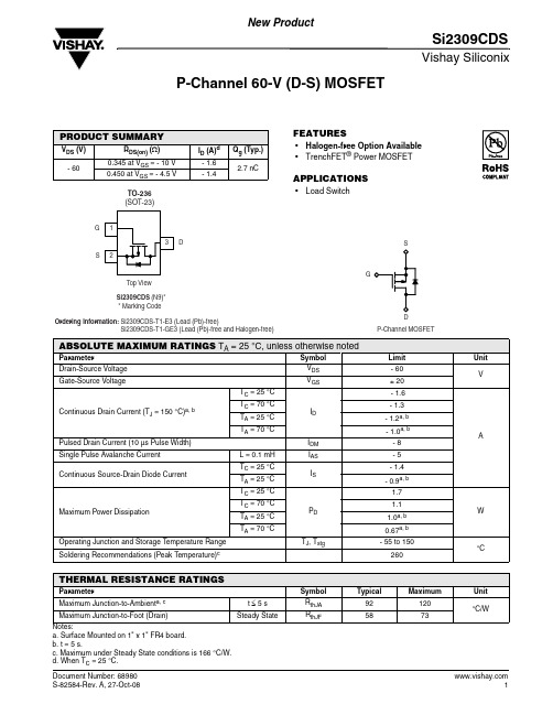
Vishay SiliconixSi2309CDSP-Channel 60-V (D-S) MOSFETFEATURES•Halogen-free Option Available •TrenchFET ® Power MOSFETAPPLICATIONS•Load SwitchPRODUCT SUMMARYV DS (V)R DS(on) (Ω)I D (A)d Q g (Typ.)- 600.345 at V GS = - 10 V - 1.6 2.7 nC0.450 at V GS = - 4.5 V- 1.4Notes:a. Surface Mounted on 1" x 1" FR4 board.b. t = 5 s.c. Maximum under Steady State conditions is 166 °C/W.d. When T C = 25 °C.ABSOLUTE MAXIMUM RATINGS T A = 25 °C, unless otherwise notedParameter Symbol Limit nitDrain-Source Voltage V DS - 60VGate-Source VoltageV GS± 20Continuous Drain Current (T J = 150 °C)a, bT C = 25 °CI D - 1.6A T C = 70 °C - 1.3T A = 25 °C - 1.2a, b T A = 70 °C- 1.0a, bPulsed Drain Current (10 µs Pulse Width)I DM - 8Single Pulse Avalanche Current L = 0.1 mH I AS - 5Continuous Source-Drain Diode CurrentT C = 25 °C I S - 1.4T A = 25 °C - 0.9a, b Maximum Power DissipationT C = 25 °CP D 1.7W T C = 70 °C 1.1T A = 25 °C 1.0a, b T A = 70 °C0.67a, b Operating Junction and Storage T emperature Range T J , T stg - 55 to 150°C Soldering Recommendations (Peak Temperature)c260THERMAL RESISTANCE RATINGSParameter Symbol Typical Maximum UnitMaximum Junction-to-Ambient a, c t ≤ 5 s R thJA 92120°C/WMaximum Junction-to-Foot (Drain)Steady StateR thJF5873Vishay SiliconixSi2309CDSNotes:a. Pulse test; pulse width ≤ 300 µs, duty cycle ≤ 2 %.b. Guaranteed by design, not subject to production testing.Stresses beyond those listed under “Absolute Maximum Ratings” may cause permanent damage to the device. These are stress ratings only, and functional operation of the device at these or any other conditions beyond those indicated in the operational sections of the specifications is not implied. Exposure to absolute maximum rating conditions for extended periods may affect device reliability.SPECIFICATIONS T J = 25 °C, unless otherwise notedParameter Symbol Test Conditions Min.Typ.Max.U nitStaticDrain-Source Breakdown Voltage V DS V GS = 0 V , I D = - 250 µA- 60V V DS Temperature Coefficient ΔV DS /T J I D = - 250 µA - 65mV/°C V GS(th) Temperature Coefficient ΔV GS(th)/T J 4.5Gate-Source Threshold Voltage V GS(th) V DS = V GS , I D = - 250 µA - 1- 3VGate-Source LeakageI GSS V DS = 0 V , V GS = ± 20 V - 100nAZero Gate Voltage Drain Current I DSS V DS = - 60 V , V GS = 0 V - 1µA V DS = - 60 V , V GS = 0 V , T J = 55 °C- 10On-State Drain Current aI D(on) V DS ≤ 5 V , V GS = - 10 V - 6A Drain-Source On-State Resistance a R DS(on) V GS = - 10 V , I D = - 1.25 A 0.2850.345ΩV GS = - 4.5 V , I D = - 1.0 A 0.3600.450Forward T ransconductance a g fsV DS = - 10 V, I D = - 1.0 A2.8SDynamic bInput Capacitance C iss V DS = - 30 V , V GS = 0 V, f = 1 MHz210pFOutput CapacitanceC oss 28Reverse Transfer Capacitance C rss 20Total Gate Charge Q g V DS = - 30 V, V GS = - 4.5 V , ID = - 1.25 A 2.7 4.1nC Gate-Source Charge Q gs 0.8Gate-Drain Charge Q gd 1.2Gate Resistance R g f = 1 MHz7ΩTurn-On Delay Time t d(on) V DD = - 30 V, R L = 30 Ω I D ≅ - 1 A, V GEN = - 4.5 V , R g = 1 Ω4060nsRise Timet r 3555Turn-Off Delay Time t d(off) 1525Fall Timet f 1020Turn-On Delay Time t d(on) V DD = - 30 V, R L = 30 ΩI D ≅ - 1 A, V GEN = - 10 V, R g = 1 Ω510Rise Timet r 1020Turn-Off Delay Time t d(off) 1525Fall Timet f1020Drain-Source Body Diode Characteristics Continuous Source-Drain Diode Current I S T C = 25 °C- 1.4A Pulse Diode Forward Current I SM - 8Body Diode VoltageV SD I S = - 0.75 A, V GS = 0 V- 0.8- 1.2V Body Diode Reverse Recovery Time t rr I F = - 1.25 A, dI/dt = 100 A/µs, T J = 25 °C3060ns Body Diode Reverse Recovery Charge Q rr 3360nC Reverse Recovery Fall Time t a 18nsReverse Recovery Rise Timet b12Gate ChargeOn-Resistance vs. Junction TemperatureSource-Drain Diode Forward VoltageThreshold VoltageSingle Pulse Power, Junction-to-AmbientVishay SiliconixSi2309CDSTYPICAL CHARACTERISTICS 25°C, unless otherwise notedVishay Siliconix maintains worldwide manufacturing capability. Products may be manufactured at one of several qualified locations. Reliability data for Silicon Technology and Package Reliability represent a composite of all qualified locations. For related documents such as package/tape drawings, part marking, and reliability data, see /ppg?68980.Normalized Thermal Transient Impedance, Junction-to-AmbientDisclaimer Legal Disclaimer NoticeVishayAll product specifications and data are subject to change without notice.Vishay Intertechnology, Inc., its affiliates, agents, and employees, and all persons acting on its or their behalf (collectively, “Vishay”), disclaim any and all liability for any errors, inaccuracies or incompleteness contained herein or in any other disclosure relating to any product.Vishay disclaims any and all liability arising out of the use or application of any product described herein or of any information provided herein to the maximum extent permitted by law. The product specifications do not expand or otherwise modify Vishay’s terms and conditions of purchase, including but not limited to the warranty expressed therein, which apply to these products.No license, express or implied, by estoppel or otherwise, to any intellectual property rights is granted by this document or by any conduct of Vishay.The products shown herein are not designed for use in medical, life-saving, or life-sustaining applications unless otherwise expressly indicated. Customers using or selling Vishay products not expressly indicated for use in such applications do so entirely at their own risk and agree to fully indemnify Vishay for any damages arising or resulting from such use or sale. Please contact authorized Vishay personnel to obtain written terms and conditions regarding products designed for such applications.Product names and markings noted herein may be trademarks of their respective owners.元器件交易网。
ltc2950的原理和应用
LTC2950的原理和应用1. LTC2950简介LTC2950是一款轻型电源管理芯片,适用于各种电池供电系统的自动开关功能。
它基于CMOS工艺,具有低功耗和高稳定性的特点。
本文将介绍LTC2950的原理和应用。
2. LTC2950的工作原理LTC2950采用了一种称为监视器模式的工作原理,其主要功能是监视系统电源电压并控制开关输出。
下面是LTC2950的工作原理:•输入电源电压监测:LTC2950能够监测输入电源的电压,并根据设定的电压阈值来确定系统是否正常工作。
当输入电压低于阈值时,LTC2950将触发系统关闭动作。
•开关输出控制:LTC2950有一个开关输出,用于控制其他外部设备的开关。
当系统运行正常时,开关输出保持开启状态;当输入电压低于阈值时,开关输出将关闭。
•自动开启恢复:LTC2950具有自动开启恢复功能,即当输入电压回复到正常范围内时,开关输出将自动开启,系统将恢复正常工作状态。
3. LTC2950的应用LTC2950的原理和功能使其在电池供电系统中具有广泛的应用。
下面是几个常见的应用场景:3.1 电池供电系统的自动开关LTC2950可以作为电池供电系统的自动开关,当电池电压低于设定阈值时,LTC2950将关闭系统以避免过放电,从而保护电池的寿命。
当电压回复正常时,LTC2950将自动开启系统,实现自动恢复。
3.2 低功耗电源管理由于LTC2950本身具有低功耗特点,可以提供给其他电路使用作为电源管理芯片。
它可以监控输入电压,根据需求控制开关输出,实现低功耗的电源管理功能。
3.3 电池充电系统LTC2950可以作为电池充电系统的控制芯片使用。
它可以监控充电电压和电流,并根据需求控制充电器的开关状态。
当充电电压和电流达到设定值时,LTC2950可以触发停止充电动作,从而保护电池的安全。
3.4 电源切换系统LTC2950还可以应用于电源切换系统中,当主电源发生故障或不稳定时,LTC2950可以自动切换到备用电源以保证系统的正常运行。
利特尔比特ltc4059 ltc4059a-900ma-线性锂离子电池充电器用热控制在2-2 dfn

124059fbInput Supply Voltage (V CC )...................... –0.3V to 10V BAT, PROG, EN, Li CC, ACPR ................... –0.3V to 10V BAT Short-Circuit Duration...........................Continuous BAT Pin Current............................................... 1000mA PROG Pin Current............................................. 1000µA Junction Temperature.......................................... 125°C Operating Temperature Range (Note 2)..–40°C to 85°C Storage Temperature Range.................–65°C to 125°CORDER PART NUMBER Consult LTC Marketing for parts specified with wider operating temperature ranges.LTC4059EDC LTC4059AEDC ABSOLUTE AXI U RATI GSW W WU PACKAGE/ORDER I FOR ATIOUUW (Note 1)T JMAX = 125°C, θJA = 60°C/W TO 85°C/W (NOTE 3)*Li CC PIN 2 ON LTC4059EDC,ACPR PIN 2 ON LTC4059AEDC EXPOSED PAD (PIN 7) IS GND MUST BE SOLDERED TO PCBTOP VIEW7DC6 PACKAGE6-LEAD (2mm × 2mm) PLASTIC DFN456321GND BAT EN PROG V CCLi CC/ACPR*DC6 PART MARKING LAFU LBJHELECTRICAL CHARACTERISTICSThe ● denotes the specifications which apply over the full operatingtemperature range, otherwise specifications are at T A = 25°C. V CC = 5V unless otherwise noted.SYMBOL PARAMETERCONDITIONSMIN TYP MAX UNITSV CC V CC Supply Voltage●3.758V I CC Quiescent V CC Supply Current V BAT = 4.5V (Forces I BAT and I PROG = 0)●2560µA I CCMS V CC Supply Current in Shutdown V EN = V CC●1025µA I CCUV V CC Supply Current in Undervoltage V CC < V BAT ; V CC = 3.5V, V BAT = 4V ●410µA LockoutV FLOAT V BAT Regulated Output Voltage I BAT = 2mA4.175 4.2 4.225V 4.5V < V CC < 8V, I BAT = 2mA● 4.158 4.2 4.242V I BAT BAT Pin CurrentR PROG = 2.43k, Current Mode, V BAT = 3.8V ●475500525mA R PROG = 12.1k, Current Mode, V BAT = 3.8V ●94100106mA I BMS Battery Drain Current in Shutdown V EN = V CC , V CC > V BAT ●0±1µA I BUV Battery Drain Current in Undervoltage V CC < V BAT , V BAT = 4V●014µA LockoutV UV V CC – V BAT Undervoltage Lockout V CC from Low to High, V BAT = 3.7V ●100150200mV ThresholdV CC from High to Low, V BAT = 3.7V ●03580mV V PROG PROG Pin VoltageR PROG = 2.43k, I PROG = 500µA ● 1.18 1.21 1.24V R PROG = 12.1k, I PROG = 100µA ● 1.18 1.21 1.24V V MS Manual Shutdown Threshold V EN Increasing ●0.30.92 1.2V V MSHYS Manual Shutdown Hysteresis V EN Decreasing 85mV R EN EN Pin Input ResistanceV EN = 5V●1 1.853M ΩV Li CC Voltage Mode Disable Threshold V Li CC Increasing (LTC4059 Only)●0.30.92 1.2V V Li CCHYS Voltage Mode Disable Hysteresis V Li CC Decreasing (LTC4059 Only)85mV V ACPR ACPR Pin Output Low Voltage I ACPR = 300µA (LTC4059A Only)0.250.5V t LIM Junction Temperature In Constant 115°C Temperature ModeR ONPower FET “ON” Resistance I BAT = 150mA (Note 4)8001200m Ω(Between V CC and BAT)Note 1: Absolute Maximum Ratings are those values beyond which the life of a device may be impaired.Note 2: The LTC4059E/LTC4059AE are guaranteed to meet performance specifications from 0°C to 70°C. Specifications over the –40°C to 85°C operating temperature range are assured by design, characterization and correlation with statistical process controls.Note 3: Failure to solder the exposed backside of the package to the PC board ground plane will result in a thermal resistance much higher than 60°C/W.Note 4: The FET on-resistance is guaranteed by correlation to wafer level measurements.3454059fbPI FU CTIO SU U UGND (P ins 1, 7): Ground/Exposed Pad. The exposed package pad is ground and must be soldered to the PC board for maximum heat transfer.Li CC (Pin 2, LTC4059): Li-Ion/Constant Current Input Pin. Pulling this pin above V Li CC disables voltage mode thereby providing a constant current to the BAT pin. This feature is useful for charging Nickel chemistry batteries.Tie to GND if unused.ACP R (P in 2, LTC4059A): Open-Drain Power Supply Status Output. When V CC is greater than the undervoltage lockout threshold, the ACPR pin will pull to ground;otherwise the pin is forced to a high impedance state.BAT (P in 3): Charge Current Output. Provides charge current to the battery and regulates the final float voltage to 4.2V. An internal precision resistor divider from this pin sets this float voltage and is disconnected in shutdown mode.V CC (P in 4): Positive Input Supply Voltage. This pin provides power to the charger. V CC can range from 3.75V to 8V. This pin should be bypassed with at least a 1µF capacitor. When V CC is within 35mV of the BAT pin voltage, the LTC4059 enters shutdown mode, dropping I BAT to less than 4µA.PROG (Pin 5): Charge Current Program and Charge Cur-rent Monitor Pin. Connecting a resistor, R PROG , to ground programs the charge current. When charging in constant-current mode, this pin servos to 1.21V. In all modes, the voltage on this pin can be used to measure the charge current using the following formula:I V R BAT PROGPROG=•1000EN (Pin 6): Enable Input Pin. Pulling this pin above the manual shutdown threshold (V MS is typically 0.92V) puts the LTC4059 in shutdown mode, thus terminating a charge cycle. In shutdown mode, the LTC4059 has less than 25µA supply current and less than 1µA battery drain current.Enable is the default state, but the pin should be tied to GND if unused.674059fbOPERATIOUThe LTC4059/LTC4059A are linear battery chargers de-signed primarily for charging single cell lithium-ion bat-teries. Featuring an internal P-channel power MOSFET,the chargers use a constant-current/constant-voltage charge algorithm with programmable current. Charge current can be programmed up to 900mA with a final float voltage accuracy of ±0.6%. No blocking diode or external sense resistor is required; thus, the basic charger circuit requires only two external components. The ACPR pin (LTC4059A) monitors the status of the input voltage with an open-drain output. The Li C C pin (LTC4059) disables constant-voltage operation and turns the LTC4059 into a precision current source capable of charging Nickel chem-istry batteries. Furthermore, the LTC4059/LTC4059A are designed to operate from a USB power source.An internal thermal limit reduces the programmed charge current if the die temperature attempts to rise above a preset value of approximately 115°C. This feature protects the LTC4059/LTC4059A from excessive temperature, and allows the user to push the limits of the power handling capability of a given circuit board without risk of damaging the LTC4059/LTC4059A or external components. Anotherbenefit of the thermal limit is that charge current can be set according to typical, not worst-case, ambient tempera-tures for a given application with the assurance that the charger will automatically reduce the current in worst-case conditions.The charge cycle begins when the voltage at the V CC pin rises approximately 150mV above the BAT pin voltage, a program resistor is connected from the PROG pin to ground, and the EN pin is pulled below the shutdown threshold (typically 0.92V).If the BAT pin voltage is below 4.2V, or the Li CC pin is pulled above V Li CC (LTC4059 only), the LTC4059 will charge the battery with the programmed current. This is constant-current mode. When the BAT pin approaches the final float voltage (4.2V), the LTC4059 enters constant-voltage mode and the charge current begins to decrease.To terminate the charge cycle the EN should be pulled above the shutdown threshold. Alternatively, reducing the input voltage below the BAT pin voltage will also terminate the charge cycle.APPLICATIO S I FOR ATIOW UUU Programming Charge CurrentThe charge current is programmed using a single resistor from the PROG pin to ground. The battery charge current is 1000 times the current out of the PROG pin. The program resistor and the charge current are calculated using the following equations:R V I I VR PROG CHG CHG PROG==10001211000121•.,•.For best stability over temperature and time, 1% metal-film resistors are recommended.The charge current out of the BAT pin can be determinedat any time by monitoring the PROG pin voltage and using the following equation:I V R BAT PROGPROG=•1000Undervoltage Lockout (UVLO)An internal undervoltage lockout circuit monitors the input voltage and keeps the charger in undervoltage lockout until V CC rises approximately 150mV above the BAT pin voltage.The UVLO circuit has a built-in hysteresis of 115mV. If the BAT pin voltage is below approximately 2.75V, then the charger will remain in undervoltage lockout until V CC rises above approximately 3V. During undervoltage lockout conditions, maximum battery drain current is 4µA.Power Supply Status Indicator (ACPR, LTC4059A Only)The power supply status output has two states: pull-down and high impedance. The pull-down state indicates that V CC is above the undervoltage lockout threshold (see Undervoltage Lockout). When this condition is not met,the ACPR pin is high impedance indicating that the LTC4059A is unable to charge the battery.894059fbPower DissipationThe conditions that cause the LTC4059/LTC4059A to reduce charge current through thermal feedback can be approximated by considering the power dissipated in the IC. For high charge currents, the LTC4059 power dissipa-tion is approximately:P D = (V CC – V BAT ) • I BATwhere P D is the power dissipated, V CC is the input supply voltage, V BAT is the battery voltage and I BAT is the charge current. It is not necessary to perform any worst-case power dissipation scenarios because the LTC4059/LTC4059A will automatically reduce the charge current to maintain the die temperature at approximately 115°C.However, the approximate ambient temperature at which the thermal feedback begins to protect the IC is:T A = 115°C – P D θJAT A = 115°C – (V CC – V BAT ) • I BAT • θJAExample: Consider an LTC4059 operating from a 5V wall adapter providing 900mA to a 3.7V Li-Ion battery. The ambient temperature above which the LTC4059/LTC4059A begin to reduce the 900mA charge current is approximately:T A = 115°C – (5V – 3.7V) • (900mA) • 50°C/W T A = 115°C – 1.17W • 50°C/W = 115°C – 59°C T A = 56°CThe LTC4059 can be used above 56°C, but the charge current will be reduced from 900mA. The approximate current at a given ambient temperature can be calculated:I C T V V BAT A CC BAT JA=°()115––•θUsing the previous example with an ambient temperature of 65°C, the charge current will be reduced to approximately:I C C V V C W CC AI mABAT BAT =°°()°=°°=11565537505065770––.•//F urthermore, the voltage at the PROG pin will change proportionally with the charge current as discussed in the Programming Charge Current section.It is important to remember that LTC4059/LTC4059A applications do not need to be designed for worst-case thermal conditions since the IC will automatically reduce power dissipation when the junction temperature reaches approximately 115°C.Board Layout ConsiderationsIn order to be able to deliver maximum charge current under all conditions, it is critical that the exposed metal pad on the backside of the LTC4059/LTC4059A package is soldered to the PC board ground. Correctly soldered to a 2500mm 2 double sided 1oz copper board the LTC4059/LTC4059A have a thermal resistance of approximately 60°C/W. F ailure to make thermal contact between the exposed pad on the backside of the package and the copper board will result in thermal resistances far greater than 60°C/W. As an example, a correctly soldered LTC4059/LTC4059A can deliver over 900mA to a battery from a 5V supply at room temperature. Without a backside thermal connection, this number could drop to less than 500mA.Stability ConsiderationsThe LTC4059 contains two control loops: constant voltage and constant current. The constant-voltage loop is stable without any compensation when a battery is connected with low impedance leads. Excessive lead length, how-ever, may add enough series inductance to require a bypass capacitor of at least 1µF from BAT to GND. Further-more, a 4.7µF capacitor with a 0.2Ω to 1Ω series resistor from BAT to GND is required to keep ripple voltage low when the battery is disconnected.High value capacitors with very low ESR (especially ce-ramic) reduce the constant-voltage loop phase margin.Ceramic capacitors up to 22µF may be used in parallel with a battery, but larger ceramics should be decoupled with 0.2Ω to 1Ω of series resistance.I n constant-current mode, the PROG pin is in the feedback loop, not the battery. Because of the additional pole created by PROG pin capacitance, capacitance on this pin must be kept to a minimum. With no additional capaci-tance on the PROG pin, the charger is stable with program resistor values as high as 12k. However, additional ca-pacitance on this node reduces the maximum allowedAPPLICATIO S I FOR ATIOW UUUFigure 5. Photo of Typical Circuit (2.5mm × 2.7mm) 1011Information furnished by Linear Technology Corporation is believed to be accurate and reliable.However, no responsibility is assumed for its use. Linear Technology Corporation makes no represen-tation that the interconnection of its circuits as described herein will not infringe on existing patent rights.121630 McCarthy Blvd., Milpitas, CA 95035-7417(408) 432-1900 ● FAX: (408) 434-0507 ● © LINEAR TECHNOLOGY CORPORA TION 2003LT/LT 0505 REV B • PRINTED IN USA。
LTC1298 微功耗双通道采样12位A D转换器演示手册说明书

1DESCRIPTIOUThe LTC ®1298 is a micropower, 11.1ksps, two-channel sampling 12-bit A/D converter that draws only 1.25mW from a single 5V supply. The LTC1298 demo board pro-vides the user with a stable and consistent platform on which to evaluate the LTC1298 A/D converter. In addition,the LTC1298 demo board illustrates the layout and by-passing techniques required to obtain optimum perfor-mance from this part. The LTC1298 demo board is de-signed to be easy to use and requires only a 7V to 15V supply, a clock signal, and an analog input signal. As shown in the Board Photo, the LTC1298 is a very space efficient solution for A/D users. By combining a mi-cropower 12-bit A/D, sample-and-hold, two-channel mul-tiplexer, serial port, and auto shutdown circuit into a single 8-pin SOIC package, all the data acquisition circuitry including the bypass caps occupy an area of only 0.1square inch.This manual shows how to use the demo board. It includes timing diagrams, power supply requirements, and analog input range information. Additionally, a schematic, parts list, drawings, and dimensions of all the PC board layers are included. Finally, an explanation of the layout andbypass strategies used in this board allows anyone de-signing a PC board to achieve maximum performance from the device.12-Bit A/D ConverterDemo Boards Proven µPower 12-Bit ADC Surface Mount Layout s On-Chip Two-Channel MulitplexersActual ADC Footprint Only 0.1 Inch 2 Including Bypass Capacitorss 71dB SINAD, 84dB THD and ±0.25LSB DNL sGerber Files for This Circuit Board Are Available.Call the LTC Factory.FEATURESTYPICAL PERFOR A CE CHARACTERISTICS A D BOARD PHOTOU UW DC045 • BP01SAMPLE FREQUENCY (Hz)0.1k11010010001k 10k 100kLT1286/98 G03S U P P L Y C U R RE N T (µA )Supply Current vs Sample Rate2DEMO MANUAL DC045W W T O P V I E WA EC 1DEMO MANUAL DC045 REFERENCEDESIGNATOR QUANTITY PART NUMBER DESCRIPTION VENDOR TELEPHONE C11TAJD476M01047µF 10V 20%, Tantalum Capacitor AVX(207) 282-5111 C2 to C5, C85GRM42-6X7R104K050AD0.1µF 50V 10%, X7R Chip Capacitor Murata Erie(814) 237-1431 C6, C9, C12312063G105ZATMA1µF 25V +80%/–20%, Y5V Chip Capacitor AVX(803) 448-9411 C71TAJB106M01010µF 10V 20%, Tantalum Capacitor AVX(207) 282-5111 C10112062R150K9BB215pF 50V 10% NPO Chip Capacitor Philips(407) 744-4200 C11108055A470GATBA47pF 50V 2% NPO Chip Capacitor AVX(803) 448-9411 D0 to D1112SF1-BR Red LED Data Display(800) 421-6815 E1, E22575-4Banana Jack Keystone(718) 956-8900 E3 to E531502-2Turret Keystone(718) 956-8900 JP11TSW-101-07-G-D Header Samtec(800) 726-8329 JP21TSW-104-07-G-D Header Samtec(800) 726-8329 JP31TSW-107-06-G-D Header Samtec(800) 726-8329 JP41TSW-105-07-G-SN Header Samtec(800) 726-8329 J11227699-3BNC Connector AMP(717) 564-0100 R1 to R1212CR32-621J-T620Ω 1/8W 5% 1206 Chip Resistor AVX(803) 448-9411 R13 to R153CT32-223J-T22k 1/8W 5% 1206 Chip Resistor AVX(803) 448-9411 R161CT32-102J-T1k 1/8W 5% 1206 Chip Resistor AVX(803) 448-9411 R171CT32-103J-T10k 1/8W 5% 1206 Chip Resistor AVX(803) 448-9411 R181CT32-5101J-T51Ω 1/8W 5% 1206 Chip Resistor AVX(803) 448-9411 S1190HBW03S DIP Switch Grayhill(708) 354-1040 U1174HC592IC Toshiba(408) 737-9844 U2174HC165IC Toshiba(408) 737-9844 U31LTC1298CS8IC LTC(408) 432-1900 U41LTC1021DCS8-5IC LTC(408) 432-1900 U5174HC14IC Texas Instruments(800) 336-5236 U61LT1121CST-5IC LTC(408) 432-1900 U7, U8274HC595IC Toshiba(408) 737-9844 4HTSP-3Plastic Stand.Micro Plastic(501) 453-88615SNT-100-BK-5Shunt Samtec(800) 726-832944/40 × 3/8Steel ScrewPARTS LISTOPERATIOUOPERATING THE BOARDPowering the BoardTo use the demo board, apply a 7V to 15V power source capable of supplying ≥100mA to the banana jacks (E1 and E2). Be careful to observe the correct polarity. On-board regulators provide 5V to the LTC1298’s V CC pin. LT1121-5 and LT1021 regulators generate 5V for the digital circuitry and ADC, respectively.Applying the Analog InputAnalog input signals are applied to the LTC1298’s two-channel (CH0 and CH1) input multiplexer through the demonstration board’s turret terminals E3 (CH0) and E4 (CH1). The input signals’ ground reference is applied to turret terminal E5. The analog signal input range is 0V to 5V. Optimum performance is achieved using a signal source that has low output impedance, is low noise, and34DEMO MANUAL DC045OPERATIOUhas low distortion. Signal generators such as the B & K Type 1051 sine generator give excellent results.Applying the Clock SignalThe clock signal is applied to BNC connector J1 and the CS signal is generated on the board. The clock input uses TTL or CMOS levels. The maximum clock frequency is 200kHz. While the clock signal is active, a high-to-low logic level transition is generated on the LTC1298’s CS input which initiates a conversion. The data transfer is shown in the timing diagrams (Figure 1).Reading the Output DataThe LTC1298 serial data outputs are buffered by the two 74HC595 latches and are available as a parallel output on connector JP3. The latches are used to drive the LEDs D0to D11. (Refer to the LTC1298 data sheet for details on different digital interface modes.)The LTC1298 output data is in unipolar format. A Data Ready line, RDY, (JP3 pin 13) is provided to latch the data.Data is valid on the rising edge of RDY. Connector JP3 has one ground pin (JP3 pin 14). Connect this pin to the data receiving system’s digital ground.MSB-First Data (MSBF = 0)Figure 1. Timing DiagramD CLKODD/ CSD LTC1286/98 • F02*AFTER COMPLETING THE DATA TRANSFER, IF FURTHER CLOCKS ARE APPLIED WITH CS LOW, THE ADC WILL OUTPUT ZEROS INDEFINITELY.ODD/ D t DATA : DURING THIS TIME, THE BIAS CIRCUIT AND THE COMPARATOR POWER DOWN AND THE REFERENCE INPUTBECOMES A HIGH IMPEDANCE NODE. WITH CS LOW AND THE CLOCK ACTIVE, THE OUTPUT ON D OUT IS EITHER LSB-FIRST DATA (MSBF = 0) OR ZEROS (MSBF = 1).MSB-First Data (MSBF = 1)5DEMO MANUAL DC045OPERATIOUTable 1.JUMPER JUMPER NAME JUMPER CONNECTIONJP1LED EnableShorted to enable LEDs. Open to disable the LEDs.JP2A CS Shorted for normal operation. If open, the CS line can be driven externally to select or deselect the LTC1286.JP2B CLK Shorted for normal operation. If open, the CLK line can be driven externally to clock the LTC1286.JP2C D OUT Shorted for normal operation. If open, the D OUT line can drive a scope probe.JP2DD INShorted for normal operation. If open, the D IN line can be driven externally to configure the input multiplexer.The LTC1298’s data word can be acquired with a logic analyzer. By using a logic analyzer that has a PC-compat-ible floppy drive, (such as an HP1663A), conversion data can be stored on a disk and easily transferred to a PC. Once the data is transfered to a PC, programs such as Mathcad or Excel can be used to calculate FFTs. The FFTs can be used to obtain LTC1298 AC specifications such as signal-to-noise ratio and total harmonic distortion.LEDs D0 to D11 provide a visual display of the LTC1298’s digital output word. D0 is the LSB and D11 is the MSB.Jumper JP1 can be removed to disable the LEDs, reducing supply consumption by up to 56mA.Driving CS, D IN , and CLKJumpers for CS, CLK, D IN , and D OUT (JP2) are shorted for normal operation. The jumpers can be removed and CS,D IN , and CLK lines can be externally driven if desired. See the LTC1298 data sheet for details on driving these YOUTThe use of separate analog and digital ground planes is a good practice for a well designed LTC1298 PC board. Theproper way to make the analog and digital ground planes can be seen by examining the solder side of the PCB layout. The two ground planes are completely isolated except for one connection at the power supply ground input, E1. The two ground planes follow the same path on the component and solder sides of the board to reduce coupling between the ground planes. Also ensure that the analog ground plane’s solder side has a limited number of plane-breaking traces within it. Any trace that opens a portion of the ground plane may reduce the ground plane’s efficiency. Further, the analog and digital traces do not cross each other (whether on the board’s top or bottom side) or run adjacent to each other.BYPASSINGIt is important to place the supply/reference bypass ca-pacitor as close as possible to the LTC1298’s supply/reference pin. The ground side of the capacitor should have a very short path to analog ground. The V CC /V REF pins should be bypassed with high quality ceramic capaci-tors of at least 0.1µF.6DEMO MANUAL DC045OPERATIOUTable 2.INPUT/OUTPUT PINFUNCTIONJ1Clock InputE1GroundE27V to 15V at ≥100mA CH0Multiplexer Input Channel 0CH1Mulitplexer Input Channel 1AGND Input signals’ ground reference JP3-1D0 (LSB)JP3-2D1JP3-3D2JP3-4D3JP3-5D4JP3-6D5INPUT/OUTPUT PINFUNCTIONJP3-7D6JP3-8D7JP3-9D8JP3-10D9JP3-11D10JP3-12D11 (MSB)JP3-13RDY. Can be used by an external system to latch the ADC’s output. Latch data on the rising edge.JP3-14Ground. Connect to the digital ground of a data receiving system.PCB LAYOUT A D FILU WComponent Side Silkscreen7DEMO MANUAL DC045Information furnished by Linear Technology Corporation is believed to be accurate and reliable.However, no responsibility is assumed for its use. Linear Technology Corporation makes no represen-tation that the interconnection of its circuits as described herein will not infringe on existing patent rights.PCB LAYOUT A D FILUWCircuit: Component SideCircuit: Solder SideComponent Side Solder MaskSolder Side Solder Mask8DEMO MANUAL DC045SYMBOL DIAMETER # OF HOLESA 0.1254B 0.2102C 0.0943D 0.035129E 0.04029F 0.0455UNMARKED0.01897TOTAL HOLES269Linear Technology Corporation1630 McCarthy Blvd., Milpitas, CA 95035-7487(408) 432-1900 qFAX : (408) 434-0507 qTELEX : 499-3977© PC FAB DRAWI GUA DAFEX8EX5F FF FAE X 14D X 128B C CC BEE NOTES:1.MATERIAL IS FR4, 0.062˝ THICK WITH 2 OUNCE COPPER.2.PCB WILL BE DOUBLE-SIDED WITH PLATED THROUGH-HOLES.3.HOLE SIZES ARE AFTER PLATING. PLATED THROUGH-HOLE WALL THICKNESS MINIMUM 0.0014˝ (1OZ.).E PADMASTER PROCESS.5.SOLDER MASK BOTH SIDES WITH PC401 USING FILM PROVIDED.6.SILKSCREEN COMPONENT SIDE USING FILM E WHITE, NON-CONDUCTIVE INK.7.ALL DIMENSIONS ARE IN INCHES.。
- 1、下载文档前请自行甄别文档内容的完整性,平台不提供额外的编辑、内容补充、找答案等附加服务。
- 2、"仅部分预览"的文档,不可在线预览部分如存在完整性等问题,可反馈申请退款(可完整预览的文档不适用该条件!)。
- 3、如文档侵犯您的权益,请联系客服反馈,我们会尽快为您处理(人工客服工作时间:9:00-18:30)。
2309fdBLOCK DIAGRAMFeAtuResAppLICAtIOnsDesCRIptIOnwith I 2C InterfacenIndustrial Process Control n Motor Controln Accelerometer Measurements n Battery-Operated Instrumentsn Isolated and/or Remote Data Acquisition nPower Supply MonitoringIntegral Nonlinearity vs Output Coden12-Bit Resolutionn Low Power: 1.5mW at 1ksps, 35µW Sleep Mode n 14ksps Throughput Rate n Low Noise: SNR = 73.4dB n Guaranteed No Missing Codes n Single 5V Supplyn 2-Wire I 2C Compatible Serial Interface with Nine Addresses Plus One Global for Synchronization n Fast Conversion Time: 1.3µs n Internal Referencen Internal 8-Channel Multiplexer n Internal Conversion Clockn Unipolar or Bipolar Input Ranges (Software Selectable)n Guaranteed Operation from –40°C to 125°C (TSSOP Package)n 24-Pin 4mm × 4mm QFN and 20-Pin TSSOP PackagesThe L TC ®2309 is a low noise, low power , 8-channel, 12-bit successive approximation ADC with an I 2C compatible serial interface. This ADC includes an internal reference and a fully differential sample-and-hold circuit to reduce common mode noise. The L TC2309 operates from an internal clock to achieve a fast 1.3µs conversion time.The L TC2309 operates from a single 5V supply and draws just 300µA at a throughput rate of 1ksps. The ADC enters nap mode when not converting, reducing the power dissipation.The L TC2309 is available in both a small 24-pin 4mm × 4mm QFN and a 20-pin TSSOP package. The internal 2.5V reference and 8-channel multiplexer further reduce PCB board space requirements.The low power consumption and small size make the L TC2309 ideal for battery-operated and portable applica-tions, while the 2-wire I 2C compatible serial interface makes this ADC a good match for space-constrained systems.L , L T , L TC, L TM, Linear Technology and the Linear logo are registered trademarks and Easy Drive is a trademark of Linear Technology Corporation. All other trademarks are the property of their respective owners.ANALOG INPUTS0V TO 4.096V UNIPOLAR ±2.048V BIPOLAROUTPUT CODE0I N L (L S B )00.250.5040962309 G01–0.25–0.50–1.00102420483072–0.751.000.75/2309fdABsOLute MAxIMuM RAtInGs (Notes 1, 2)ORDeR InFORMAtIOnLEAD FREE FINISH TAPE AND REEL PART MARKING*PACKAGE DESCRIPTIONTEMPERATURE RANGE L TC2309CUF#PBF L TC2309CUF#TRPBF 230924-Lead (4mm × 4mm) Plastic QFN 0°C to 70°C L TC2309IUF#PBF L TC2309IUF#TRPBF 230924-Lead (4mm × 4mm) Plastic QFN –40°C to 85°C L TC2309CF#PBF L TC2309CF#TRPBF L TC2309F 20-Lead Plastic TSSOP 0°C to 70°C L TC2309IF#PBF L TC2309IF#TRPBF L TC2309F 20-Lead Plastic TSSOP –40°C to 85°C L TC2309HF#PBFL TC2309HF#TRPBFL TC2309F20-Lead Plastic TSSOP–40°C to 125°CConsult L TC Marketing for parts specified with wider operating temperature ranges. *The temperature grade is identified by a label on the shipping container .Consult L TC Marketing for information on non-standard lead based finish parts.For more information on lead free part marking, go to: http://www.linear .com/leadfree/For more information on tape and reel specifications, go to: http://www.linear .com/tapeandreel/Supply VoltageV D D ..........................................................–0.3V to 6V Analog Input Voltage (Note 3) CH0-CH7, COM, V REF ,REFCOMP ....................(GND – 0.3V) to (V DD + 0.3V)Digital Input Voltage (Note 3) ............................(GND – 0.3V) to (V DD + 0.3V)Digital Output Voltage ......(GND – 0.3V) to (V DD + 0.3V)Power Dissipation ..............................................500mW Operating Temperature RangeLTC2309C ................................................0°C to 70°C LTC2309I .............................................–40°C to 85°C LTC2309H ..........................................–40°C to 125°C Storage Temperature Range ..................–65°C to 150°C Lead Temperature (Soldering, 10 sec)TSSOP ..............................................................300°CpIn COnFIGuRAtIOn/2309fdCOnVeRteR AnD MuLtIpLexeR CHARACteRIstICsPARAMETERCONDITIONSMIN TYP MAX UNITS Resolution (No Missing Codes)l12Bits Integral Linearity Error (Note 6)l ±0.45±1LSB Differential Linearity Error l ±0.35±1LSB Bipolar Zero Error (Note 7)l±1±8LSB Bipolar Zero Error Drift 0.002LSB/°C Bipolar Zero Error Match ±0.1±3LSB Unipolar Zero Error (Note 7)l±0.4±6LSB Unipolar Zero Error Drift 0.002LSB/°C Unipolar Zero Error Match ±0.2±1LSB Bipolar Full-Scale Error External Reference (Note 8) REFCOMP = 4.096V l l±0.5 ±0.4±10 ±9LSB LSB Bipolar Full-Scale Error Drift External Reference0.05LSB/°C Bipolar Full-Scale Error Match ±0.4±3LSB Unipolar Full-Scale ErrorQFN External Reference (Note 8) TSSOP External Reference (Note 8)l l ±0.4 ±0.5±10 ±12LSB LSB REFCOMP = 4.096V l±0.3±6LSB Unipolar Full-Scale Error Drift External Reference0.05LSB/°C Unipolar Full-Scale Error Match±0.3±2LSBThe l denotes the specificationswhich apply over the full operating temperature range, otherwise specifications are at T A = 25°C. (Notes 4, 5)SYMBOL PARAMETERCONDITIONS MIN TYPMAX UNITSV IN +Absolute Input Range (CH0 to CH7)(Note 9)l –0.05REFCOMP V V IN –Absolute Input Range (CH0 to CH7, COM)Unipolar (Note 9) Bipolar (Note 9)l l –0.05 –0.050.25 • REFCOMP 0.75 • REFCOMPV V V IN + – V IN –Input Differential Voltage Range V IN = V IN + – V IN – (Unipolar) V IN = V IN + – V IN – (Bipolar)l l 0 to REFCOMP ±REFCOMP/2V V I IN Analog Input Leakage Current l±1µA C IN Analog Input CapacitanceSample Mode Hold Mode55 5pF pF CMRRInput Common Mode Rejection Ratio70dBAnALOG InputThe l denotes the specifications which apply over the full operating temperature range, otherwisespecifications are at T A = 25°C. (Note 4)SYMBOL PARAMETERCONDITIONS MIN TYP MAXUNITS SINAD Signal-to-(Noise + Distortion) Ratio f IN = 1kHz l 7173.3dB SNR Signal-to-Noise Ratio f IN = 1kHzl 7173.4dB THD Total Harmonic Distortion f IN = 1kHz, First 5 Harmonics l –88–77dB SFDRSpurious Free Dynamic Range f IN = 1kHz l7990dB Channel-to-Channel Isolation f IN = 1kHz –109dB Full Linear Bandwidth(Note 11)700kHz –3dB Input Linear Bandwidth 25MHz Aperture Delay 13ns T ransient ResponseFull-Scale Step240nsDYnAMIC ACCuRACYThe l denotes the specifications which apply over the full operating temperature range,otherwise specifications are at T A = 25°C. A IN = –1dBFS. (Notes 4, 10)/2309fdpOWeR ReQuIReMentsPARAMETERCONDITIONS MIN TYP MAX UNITSV REF Output Voltage I OUT = 0 (QFN) I OUT = 0 (TSSOP)l l2.47 2.462.50 2.50 2.53 2.54V V V REF Output Tempco I OUT = 0±25ppm/°CV REF Output Impedance –0.1mA ≤ I OUT ≤ 0.1mA 8kΩV REFCOMP Output Voltage I OUT = 04.096V V REF Line RegulationV DD = 4.75V to 5.25V0.8mV/VInteRnAL ReFeRenCe CHARACteRIstICsThe l denotes the specifications which apply over the fulloperating temperature range, otherwise specifications are at T A = 25°C. (Note 4)I2C Inputs AnD DIGItAL Outputs The l denotes the specifications which apply over the fulloperating temperature range, otherwise specifications are at T A = 25°C. (Note 4)SYMBOL PARAMETERCONDITIONSMIN TYP MAX UNITSV IH High Level Input Voltage l 2.85V V IL Low Level Input Voltagel 1.5V V IHA High Level Input Voltage for Address Pins A1, A0l 4.75V V ILA Low Level Input Voltage for Address Pins A1, A0l 0.25V R INH Resistance from A1, A0, to V DD to Set Chip Address Bit to 1l 10kΩR INL Resistance from A1, A0 to GND to Set Chip Address Bit to 0l 10kΩR INF Resistance from A1, A0 to GND or V DD to Set Chip Address Bit to Float l2MΩI I Digital Input CurrentV IN = V DD l –1010µA V HYS Hysteresis of Schmitt T rigger Inputs (Note 9)l 0.25V V OL Low Level Output Voltage (SDA)I = 3mA l 0.4V t OF Output Fall Time V H to V IL(MAX)(Note 12)l 20 + 0.1C B250ns t SP Input Spike Suppressionl 50ns C CAXExternal Capacitance Load On-Chip Address Pins (A1, A0) for Valid Floatl 10pFSYMBOL PARAMETER CONDITIONSMIN TYP MAX UNITSV DD Supply Voltage l4.755 5.25V I DDSupply Current 14ksps Sample Ratel 2.33mA Nap Mode SLP Bit = 0, Conversion Done l 210350µA Sleep ModeSLP Bit = 1, Conversion Done l 715µA P DPower Dissipation 14ksps Sample Ratel 11.515mW Nap Mode SLP Bit = 0, Conversion Done l 1.05 1.75mW Sleep ModeSLP Bit = 1, Conversion Donel3575µWThe l denotes the specifications which apply over the full operating temperature range, otherwise specifications are at T A = 25°C. (Note 4)/I2C tIMInG CHARACteRIstICs The l denotes the specifications which apply over the full operating temperature range, otherwise specifications are at T A = 25°C. (Note 4)SYMBOL PARAMETER CONDITIONS MIN TYP MAX UNITS f SCL SCL Clock Frequency l400kHz t HD(SDA)Hold Time (Repeated) START Condition l0.6µs t LOW LOW Period of the SCL Pin l 1.3µs t HIGH HIGH Period of the SCL Pin l0.6µs t SU(STA)Set-Up Time for a Repeated START Condition l0.6µs t HD(DAT)Data Hold Time l00.9µs t SU(DAT) Data Set-Up Time l100ns t r Rise Time for SDA/SCL Signals(Note 12)l20 + 0.1C B300ns t f Fall Time for SDA/SCL Signals(Note 12)l20 + 0.1C B300ns t SU(STO)Set-Up Time for STOP Condition l0.6µs t BUF Bus Free Time Between a STOP and START Condition l 1.3µs ADC tIMInG CHARACteRIstICs The l denotes the specifications which apply over the full operating temperature range, otherwise specifications are at T A = 25°C. (Note 4)SYMBOL PARAMETER CONDITIONS MIN TYP MAX UNITS f SMPL Throughput Rate (Successive Reads)l14ksps t CONV Conversion Time(Note 9)l 1.3 1.8µs t ACQ Acquisition Time(Note 9)l240ns t REFWAKE REFCOMP Wake-Up Time (Note 13)C REFCOMP = 10µF, C REF = 2.2µF200msNote 1: Stresses beyond those listed under Absolute Maximum Ratings may cause permanent damage to the device. Exposure to any Absolute Maximum Rating condition for extended periods may affect device reliability and lifetime.Note 2: All voltage values are with respect to ground.Note 3: When these pin voltages are taken below ground or above V DD, they will be clamped by internal diodes. These products can handle input currents greater than 100mA below ground or above V DD without latchup. Note 4: V DD = 5V, f SMPL = 14ksps internal reference unless otherwise noted.Note 5: Linearity, offset and full-scale specifications apply for a single-ended analog input with respect to COM.Note 6: Integral nonlinearity is defined as the deviation of a code from a straight line passing through the actual endpoints of the transfer curve. The deviation is measured from the center of the quantization band. Note 7: Bipolar zero error is the offset voltage measured from –0.5LSB when the output code flickers between 0000 0000 0000 and 1111 1111 1111. Unipolar zero error is the offset voltage measured from +0.5LSB when the output code flickers between 0000 0000 0000 and 0000 0000 0001.Note 8: Full-scale bipolar error is the worst-case of –FS or +FS untrimmed deviation from ideal first and last code transitions and includes the effect of offset error. Unipolar full-scale error is the deviation of the last code transition from ideal and includes the effect of offset error.Note 9: Guaranteed by design, not subject to test.Note 10: All specifications in dB are referred to a full-scale ±2.048V input with a 2.5V reference voltage.Note 11: Full linear bandwidth is defined as the full-scale input frequency at which the SINAD degrades to 60dB or 10 bits of accuracy.Note 12: C B = capacitance of one bus line in pF (10pF ≤ C B ≤ 400pF). Note 13: REFCOMP wake-up time is the time required for the REFCOMP pin to settle within 0.5LSB at 12-bit resolution of its final value after waking up from SLEEP mode./2309fdtYpICAL peRFORMAnCe CHARACteRIstICsIntegral Nonlinearity vs Output Code 1kHz Sine Wave 8192 Point FFT PlotSupply Currentvs Sampling Frequency Offset Error vs Temperature Full-Scale Error vs TemperatureSupply Current vs Temperature Sleep Current vs Temperature Analog Input Leakage Current vs TemperatureT A = 25°C, V DD = 5V, f SMPL = 14ksps, unless otherwise noted.Differential Nonlinearityvs Output CodeOUTPUT CODEINL(LSB)0.250.5040962309 G01–0.25–0.50–1.00102420483072–0.751.000.75OUTPUT CODEDNL(LSB)0.250.5040962309 G02–0.25–0.50–1.00102420483072–0.751.000.75FREQUENCY (kHz)–140MAGNITUDE(dB)–120–100–80–4013472309 G03–20–60256SNR = 73.4dBSINAD = 73.3dBTHD = –88dB SAMPLING FREQUENCY (ksps)0.1SUPPLYCURRENT(mA)1.52.02.51101003209 G041.00.5TEMPERATURE (°C)–50OFFSETERROR(LSB)1.5252309 G05–1.0–25050–0.5–2.02.01.00.5–0.575100125TEMPERATURE (°C)–6FULL-SCALEERROR(LSB)–242309 G06–42100UNIPOLARBIPOLARTEMPERATURE (°C)–501.0SUPPLYCURRENT(mA)1.21.61.82.03.02.4050752309 G071.42.62.82.2–2525100125TEMPERATURE (°C)LEAKAGECURRENT(nA)10030040050010007002309 G09200800900600–25TEMPERATURE (°C)–50–25SLEEPCURRENT(µA)410050752309 G0828625100125/2309fdpIn FunCtIOnsCH3-CH7 (Pins 1-5): Channel 3 to Channel 7 Analog Inputs. CH3-CH7 can be configured as single-ended or differential input channels. See the Analog Input Multiplexer section.COM (Pin 6): Common Input. This is the reference point for all single-ended inputs. It must be free of noise and should be connected to ground for unipolar conversions and midway between GND and REFCOMP for bipolar conversions.V REF (Pin 7): 2.5V Reference Output. Bypass to GND with a minimum 2.2µF ceramic capacitor. The internal reference may be overdriven by an external 2.5V refer-ence at this pin.REFCOMP (Pin 8): Reference Buffer Output. Bypass to GND with 10µF and 0.1µF ceramic capacitors in parallel. Nominal output voltage is 4.096V. The internal reference buffer driving this pin is disabled by ground-ing V REF , allowing REFCOMP to be overdriven by an external source.GND (Pins 9-11, 18-20): Ground. All GND pins must be connected to a solid ground plane.V DD (Pins 12, 13, 21): 5V Supply. The range of V DD is 4.75V to 5.25V. Bypass V DD to GND with a 10µF ceramic capacitor in parallel with three 0.1µF ceramic capacitors, one located as close as possible to each pin.AD0 (Pin 14): Chip Address Control Pin. This pin is configured as a three-state (LOW, HIGH, floating) ad-dress control bit for the device I2C address. See Table 2 for address selection.AD1 (Pin 15): Chip Address Control Pin. This pin is configured as a three-state (LOW, HIGH, floating) address control bit for the device I2C address. See Table 2 for address selection.SCL (Pin 16): Serial Clock Pin of the I2C Interface. The L TC2309 can only act as a slave and the SCL pin only accepts an external serial clock. Data is shifted into the SDA pin on the rising edges of the SCL clock and output through the SDA pin on the falling edges of the SCL clock.SDA (Pin 17): Bidirectional Serial Data Line of the I2C Interface. In transmitter mode (read), the conversion result is output at the SDA pin, while in receiver mode (write), the D IN word is input at the SDA pin to con-figure the ADC. The pin is high impedance during the data input mode and is an open-drain output (requires an appropriate pull-up device to V DD) during the data output mode.CH0-CH2 (Pins 22-24): Channel 0 to Channel 2 Analog Inputs. CH0-CH2 can be configured as single-ended or differential input channels. See the Analog Input Multiplexer section.Exposed Pad (Pin 25): Ground. Must be soldered directly to ground plane.(QFN)/2309fdpIn FunCtIOnsREFCOMP (Pin 1): Reference Buffer Output. Bypass to GND with 10µF and 0.1µF ceramic capacitors in parallel. Nominal output voltage is 4.096V. The internal reference buffer driving this pin is disabled by ground-ing V REF , allowing REFCOMP to be overdriven by an external source.GND (Pins 2, 8 , 9): Ground. All GND pins must be connected to a solid ground plane.V DD (Pins 3, 10): 5V Supply. The range of V DD is 4.75V to 5.25V. Bypass V DD to GND with a 10µF ceramic ca-pacitor in parallel with two 0.1µF ceramic capacitors, one located as close as possible to each pin.AD0 (Pin 4): Chip Address Control Pin. This pin is con-figured as a three-state (LOW, HIGH, floating) address control bit for the device I2C address. See Table 2 for address selection.AD1 (Pin 5): Chip Address Control Pin. This pin is configured as a three-state (LOW, HIGH, floating) address control bit for the device I2C address. See Table 2 for address selection.SCL (Pin 6): Serial Clock Pin of the I2C Interface. The L TC2309 can only act as a slave and the SCL pin only accepts an external serial clock. Data is shifted into the SDA pin on the rising edges of the SCL clock and output through the SDA pin on the falling edges of the SCL clock.SDA (Pin 7): Bidirectional Serial Data Line of the I2C Interface. In transmitter mode (read), the conversion result is output at the SDA pin, while in receiver mode (write), the D IN word is input at the SDA pin to con-figure the ADC. The pin is high impedance during the data input mode and is an open-drain output (requires an appropriate pull-up device to V DD) during the data output mode.CH0-CH7 (Pins 11-18): Channel 0 to Channel 7 Analog Inputs. CH0-CH7 can be configured as single-ended or differential input channels. See the Analog Input Multiplexer section.COM (Pin 19): Common Input. This is the reference point for all single-ended inputs. It must be free of noise and should be connected to ground for unipolar conversions and midway between GND and REFCOMP for bipolar conversions.V REF (Pin 20): 2.5V Reference Output. Bypass to GND with a minimum 2.2µF ceramic capacitor. The internal reference may be overdriven by an external 2.5V refer-ence at this pin.(TSSOP)/2309fdFunCtIOnAL BLOCK DIAGRAMCH0 CH1 CH2 CH3 CH4 CH5 CH6 CH7 COMV REFtIMInG DIAGRAMDefinition of Timing for Fast/Standard Mode Devices on the I2C BusSDASCLS = START, Sr = REPEATED START, P = STOPt/2309fdAppLICAtIOns InFORMAtIOnOverviewThe L TC2309 is a low noise, 8-channel, 12-bit succes-sive approximation register (SAR) A/D converter with an I2C compatible serial interface. The L TC2309 includes a precision internal reference and a configurable 8-chan-nel analog input multiplexer (MUX). The ADC may be configured to accept single-ended or differential signals and can operate in either unipolar or bipolar mode. A sleep mode option is also provided to further reduce power during inactive periods.The L TC2309 communicates through a 2-wire I2C compatible serial interface. Conversions are initiated by signaling a STOP condition after the part has been successfully addressed for a read/write operation. The device will not acknowledge (NACK) an external request until the conversion is finished. After a conversion is finished, the device is ready to accept a read/write request. Once the L TC2309 is addressed for a read operation, the device begins outputting the conver-sion result under the control of the serial clock (SCL). There is no latency in the conversion result. There are 12 bits of output data followed by 4 trailing zeros. Data is updated on the falling edges of SCL, allowing the user to reliably latch data on the rising edge of SCL. A write operation may follow the read operation by using a repeat START or a STOP condition may be given to start a new conversion. By selecting a write operation, the ADC can be programmed with a 6-bit D IN word. The D IN word configures the MUX and programs various modes of operation of the ADC.During a conversion, the internal 12-bit capacitive charge redistribution DAC output is sequenced through a successive approximation algorithm by the SAR start-ing from the most significant bit (MSB) to the least significant bit (LSB). The sampled input is successively compared with binary weighted charges supplied by the capacitive DAC using a differential comparator. At the end of a conversion, the DAC output balances the analog input. The SAR contents (a 12-bit data word) that represent the sampled analog input are loaded into 12 output latches that allow the data to be shifted out via the I2C interface.Programming the L TC2309The various modes of operation of the L TC2309 are programmed by a 6-bit D IN word. The SDI input data bits are loaded on the rising edge of SCL during a write operation, with the S/D bit loaded on the first rising edge and the SLP bit on the sixth rising edge (see Figure 8b in the I2C Interface section). The input data word is defined as follows:S/D O/S S1S0UNI SLPS/D = SINGLE-ENDED/DIFFERENTIAL BITO/S = ODD/SIGN BITS1 = CHANNEL SELECT BIT 1S0 = CHANNEL SELECT BIT 0UNI = UNIPOLAR/BIPOLAR BITSLP = SLEEP MODE BITAnalog Input MultiplexerThe analog input MUX is programmed by the S/D, O/S, S1 and S0 bits of the D IN word. Table 1 lists the MUX configurations for all combinations of the con-figuration bits. Figure 1a shows several possible MUX configurations and Figure 1b shows how the MUX can be reconfigured from one conversion to the next. Driving the Analog InputsThe analog inputs of the L TC2309 are easy to drive. Each of the analog inputs can be used as a single-ended input relative to the COM pin (CH0-COM, CH1-COM, etc.) or in differential input pairs (CH0 and CH1, CH2 and CH3, CH4 and CH5, CH6 and CH7). Figure 2 shows how to drive COM for single-ended inputs in unipolar and bipolar modes. Regardless of the MUX configura-tion, the “+” and “–” inputs are sampled at the same instant. Any unwanted signal that is common to both inputs will be reduced by the common mode rejection of the sample-and-hold circuit. The inputs draw only one small current spike while charging the sample-and-hold capacitors during the acquire mode. In conversion/02309fd分销商库存信息:LINEAR-TECHNOLOGYLTC2309CUF#PBF LTC2309IUF#PBF LTC2309HF#PBF LTC2309CUF#TRPBF LTC2309CF#PBF LTC2309CF#TRPBF LTC2309IF#PBF LTC2309HF#TRPBF LTC2309IF#TRPBF LTC2309IUF#TRPBF DC1337A。