PYX28C64-35CWMB中文资料
Datasheet MLX90614 中文 数据手册 rev008

单区视场和双区视场 TO-39 封装 红外温度传感器
特性和优点
尺寸小,成本低 易集成 在极宽温度范围内工作,带出厂校准: 传感器工作温度范围:-40…+125˚C 被测目标温度范围:-70…+380˚C Ta 和 To 在 0 到 50° C 时,测量精度可达 0.5° C 高(医疗)精度校准 测量值分辨率 0.02° C 单区视场和双区视场可选 SMBus 兼容数字接口 可配置 PWM 连续输出 3V 或 5V 供电,也可使用 8…16V 供电调制 支持睡眠模式 适合不同应用领域的多种封装方式和测试方式 车用级别标准
3901090614 Rev 008
第 2ห้องสมุดไป่ตู้/ 52 页
数据手册 2013/2/28
MLX90614 系列
单区视场和双区视场 TO-39 封装 红外温度传感器
3 目录
1 功能图 ........................................................................................................................................................................................................ 1 2 概述 ......................................................................................................................................................................
YXC编程器详细说明书样本

YX-C多功能编程器YX-C多功能编程器是咱们依照国外资料仿制一种便宜、功能繁多普及型编程器。
YX-C多功能编程器通过并口与PC连接,支持Win9x、Me、XP、NT以及操作系统;英文软件(性能稳定),适合电脑公司、电子兴趣者、电子产品维修等工作人员使用。
使用前只需要将“YX-C程序”复制到电脑硬盘中即可。
打开文献夹“YX-C程序”,双击“EpromM51.exe”一、软件运营窗口如下:二、菜单栏:1、File(文件):下拉菜单中Load打开需要编程文献。
下拉菜单中Save as‥另存为编程器读入文献作为备用。
下拉菜单中Exit为退出程序。
2、Edit(编辑):编辑数据。
3、Device(选取元件):选取芯片类型。
4、Action(操作):对芯片进行操作,如:读写、编程/RAM测试、比较/校验、空白检查、擦除芯片、获取ID、清空缓存、颠倒数据、互换字节等。
5、Help(帮助):联机测试等。
6、主窗口简介:三、工具栏:1、打开文献。
把编译好数据调入编程器中。
可以打开文献类型为:二进制(*.BIN)、十六进制(*.HEX)等。
2、另存为一种文献。
把正在编辑中数据此外保存为一种*.bin文献。
3、清除缓存。
4、读取芯片数据。
5、校验数据。
6、空白测试。
检测芯片存储器与否为空。
7、获取芯片ID。
8、芯片编程。
9、擦除(清空)芯片。
四、支持芯片列表EPROM :27C16、27C32、27C64、27C128、27C256、27C512、27C010、27C020、27C040、27C1001 M27C1001、M27C、M27C400127C080,M27C801,M87C2572716(Vpp25V)、2732、2764、27128、27256、27512、27010FLASH Memory :28F64、28F128、28F256、28F512、28F010、28F020MX26C1000、MX26C、MX28F1000、MX28FAm28F256A、Am28F512A、Am28F010A、Am28F020AIntel:i28F001BX、28F004、28F008、28F016SST28SF040A 、LE28F400129F64、29F128、29F256、29F512、29F010、29F020、29F040、29F08029F001、29F002、29F004、29F008、29F016、29F032AT29C256、AT29C512、AT29C010A、AT29C020、AT29C040、AT29C040AW29EE512、W29EE011、W29EE012、W29C020(128)、W29C040PH29EE010(W29EE011)ASD AE29F1008 (AT29C010)、AE29F (AT29C020)AT49F512、AT49F010、AT49F020、AT49F040SST39SF010、SST3S9F020 、SST39SF040AT49F001、AT49F002 、AT49F008AAm29F512、Am29F010、Am29F020、Am29F040、HY29F08029F002、29F002T、Pm29F002TEEPROM :28C65、28C64、28C128、28C256、28C512、28C010、28C020、28C040 M28C16A/17A (DIP28)28C16、XLS2816 (DIP24)AT28C64B、AT28C256、AT28C512、AT28C010、AT28C020、AT28C040电擦 EPROM :W27E512、W27E010、W27C010、W27C020、W27C040SST27SF256、SST27SF512、SST27SF010、SST27SF020MX26C4000Vcc = 3.3-3.6V SST37VF512、SST37VF010、SST37VF020、SST37VF040串行(I2C) EEPROM :24C02、24C04、24C08、24C16、85C72、85C82、85C9224C32、24C64、24C128、24C256、24C512 (所有C、LC系列)PCF8572 或8572,PCF8582或8582,PCF8592或8592Microwire EEPROM :8位模式:93C06、93C46、93LC46、93C56、93C57、93C66、93C76、93C86、93C13、93C1416位模式:AT59C11、AT59C22、AT59C13CAT35C102、CAT35C104、CAT35C10893C06A 、93C46X、93C56、93C66、93C76、93C86 (NS)SPI EEPROM :Atmel:AT25010、020、040 (A8-A0)AT25080、160、320、640、128、256 (A15-A0)ST:W95010....256、Microchip 25x010 - 25x64025010、25020、2504025C080、25C160、25C320、25C640、25C128、25C256、25C512AT25HP256、AT25HP512AT25HP1024CAT64LCxxx (16位数据I/O)CAT64LC010、CAT64LC020、CAT64LC040PIC单片机:17XXX、18XXX系列16C84,16F84,16F84A ,16F627/16F62812C508/A,12C509/A,12CE518,12CE519,16C50516C620 16C621,16C622,16CE623,16CE624,16CE625,16C710/71151系列单片机(需要51AVR适配器) :AT89C51、52、55、AT89LV51、52、55AT89S51、AT89S52、AT89S53、AT89LS51、AT89LS52、AT89SL53AT89S8252 (8K+2K)、AT89LS8252、AT89LS53AT89C1051、AT89C2051、AT89C4051 (20pin)AT89C51RC (32KB)、AT89C55WD (6.2V)AT89LV52,AT89C55,AT89LV55 AT89S8252,AT89LS8252,AT89S53,AT89LS53 AT87F51,AT87F52 i87C51、i87C51FA、i87C51FBi8xC51、i8xC52、i8xC54、i8xC58i87C51,i87C51FA,i87C51FB,i87C51FC,i87C52,i87C54,i87C58 AT89C51RC (32KB),AT89C55WD等AT90S1200、AT90S231390S2333、90S4433、90S4414、90S8515、90S4434、90S8535,AT90S2313四、举例操作阐明使用编程器对W27C020进行读、擦除和写1、打开文献夹“YX-C程序”,双击“EpromM51.exe”操作软件运营窗口如下:2、用鼠标点击“Device”,在下拉菜单中点击“EPROM Electrical Erase”,再在下拉菜单中点击“Winboad 27E/27C”,最后在下拉菜单中点击“W27x020 (Vpe=14V)”。
DSC100 中文手册
2.2.2 报警逻辑...............................................................................................................................11
2.2.3 故障逻辑...............................................................................................................................13
2.2
停车,报警和故障逻辑 ....................................................................................11
2.2.1 停车逻辑...............................................................................................................................11
文档号 No. 001 中国 北京 印制
目录
目录......................................................................................................................................................................... i
产品和培训信息 .............................................................................................................................................v
广州唯创电子 WTB 系列语音芯片说明书
WTB系列语音芯片使用说明书目录1、WTB芯片特征 (3)2、应用范围 (3)3、WTB系列语音芯片选型 (3)4、WTB系列语音芯片应用方框图 (4)5、封装示意图 (4)6、管脚描述 (5)6.1、WTB015/031-16P封装引脚对应表 (5)6.2、WTB015-18S封装引脚对应表 (5)6.3、WTB031-18S封装引脚对应表 (6)6.4、WTB084-20SS/20P封装引脚对应表 (7)7、电器参数 (8)8、环境绝对极限参数 (8)9、定义IO口 (9)10、控制模式 (9)10.1、按键控制模式 (9)10.1.1、脉冲可重复触发 (9)10.1.2、脉冲不可重复触发 (9)10.1.3、电平保持可循环触发 (10)10.1.4、电平保持不可循环触发 (10)10.1.5、下一曲触发 (10)10.1.6、上一曲触发 (10)10.1.7、播放/停止触发 (11)10.1.8、播放/暂停触发 (11)10.2、一线串口控制模式 (11)10.2.1、端口分配表 (11)10.2.2、发送8位数据控制形式语音地址对应关系 (12)10.2.3、发送8位数据控制形式控制时序图 (12)10.2.4、发送16位数据控制形式语音地址对应关系 (12)10.2.5、发送16位数据控制形式控制时序图 (13)10.3、三线串口控制模式 (13)10.3.1、端口分配方式 (13)10.3.2、语音地址对应关系 (13)10.3.3、三线串口控制时序 (14)11、典型应用电路 (14)11.1、WTB015/031-16P (14)11.1.1、WTB015/031-16P按键控制(PWM输出)应用电路 (14)11.1.2、WTB015/031-16P按键控制(DAC输出)应用电路 (15)11.1.3、WTB015/031-16P一线串口控制(PWM输出)应用电路 (15)11.1.4、WTB015/031-16P一线串口控制(DAC输出)应用电路 (15)11.1.5、WTB015/031-16P三线串口控制(PWM输出)应用电路 (16)11.1.6、WTB015/031-16P三线串口控制(DAC输出)应用电路 (16)11.2、WTB015/031-18S (16)11.2.1、WTB015/031-18S按键控制(PWM输出)应用电路 (16)11.2.2、WTB031-18S按键控制(DAC输出)应用电路 (17)11.2.3、WTB015/031-18S一线串口控制(PWM输出)应用电路 (17)11.2.4、WTB015/031-18S一线串口控制(DAC输出)应用电路 (17)11.2.5、WTB015/031-18S三线串口(PWM输出)应用电路 (18)11.2.6、WTB015/031-18S三线串口(DAC输出)应用电路 (18)11.3、WTB084-20SS/20P (19)11.3.1、WTB084-20SS/20P按键控制(PWM输出)应用电路 (19)11.3.2、WTB084-20SS/20P按键控制(DAC输出)应用电路 (19)11.3.3、WTB084-20SS/20P一线串口(PWM输出)应用电路 (19)11.3.4、WTB084-20SS/20P一线串口(DAC输出)应用电路 (20)11.3.5、WTB084-20SS/20P三线串口(PWM输出)应用电路 (20)11.3.6、WTB084-20SS/20P三线串口(DAC输出)应用电路 (20)12、应用范例电路 (21)12.1、电动车应用电路 (21)12.2、定时药盒应用电路 (22)13、控制程序范例 (22)13.1、一线串口(发送8位数据控制形式)控制程序范例 (22)13.2、一线串口(发送16位数据控制形式)控制程序范例 (24)13.3、三线串口控制程序范例 (27)14、封装尺寸 (29)14.1、WTB015/031-16P封装尺寸 (29)14.2、WTB015/031-18S封装尺寸 (30)15、货源信息 (31)16、说明书版本记录 (31)1、WTB芯片特征WTB语音芯片是一款低成本OTP语音芯片;工业级性能,确保产品在多种场合下正常工作;内置音频合成器的4位微型语音处理器及4位数字逻辑运算器;WTB语音芯片完备的内部资源包括EPROM、RAM和I/O端口等;可定义多路输入端和输出端;随意定义控制输入端触发功能;自动休眠功能,有效降低功耗;支持WAV音频和两通道MIDI播放;可工作于4MHz和8MHz两种震荡模式,不同模式下的音频最高采样率分别为14KHz和28KHz;WTB系列语音芯片包括WTB015、WTB031、WTB084、WTB170,其存储时间分别为15秒、31秒、84秒、170秒,目前库存有WTB015、WTB031和WTB084三种;可加载128段语音进行控制播放;单芯片方案,可掩膜投产,降低批量生产成本;支持9bit D/A和8bit PWM输出;工作电压:DC2.2V~5.5V。
PY264-35WM中文资料

Document # EPROM102 REV ORPY2648K X 8 REPROGRAMMABLE PROMDESCRIPTIONThe PY264 is an 8Kx8 CMOS PROM. The device is available in windowed packages which when exposed to UV light, the memory content in the PROM is erased and can be reprogrammed. EPROM technology is used in the memory cells for programming. The EPROM re-quires a 12.5V for programming. Devices are tested to insure that performance of the device meets the DC and AC specification limits after customer programming.To perform a read operation from the device, CS is LOW.The memory contents in the address established by the Address pins (A 0 to A 12) will become available on the outputs (O 0 to O 7).The PY264 is available in 24-pin 600 mil Ceramic DIPs (Windowed) and Plastic DIPs (Non-Windowed).FUNCTIONAL BLOCK DIAGRAMPIN CONFIGURATIONFEATURESEPROM Technology for reprogramming High Speed– 35/45/55 ns (Commercial)– 35/45/55 ns (Military)Low Power Operation:– 660 mW Commercial – 770 mW MilitarySingle 5V±10% Power SupplyWindowed devices for reprogramming Fully TTL Compatible Inputs and Outputs Standard Pinout (JEDEC Approved):– 24-Pin 600 mil Windowed CERDIP– 24-Pin 600 mil Non-Windowed Plastic DIPDIP (P8, WD2)Note: Window on WD2 package onlyPY264MAXIMUM RATINGS (1)Symbol Parameter Value Unit V CCPower Supply Pin with –0.5 to +7VRespect to GND Terminal Voltage with –0.5 to V TERM Respect to GND V CC +0.5V (up to 7.0V)V PPProgram Voltage13VSymbol ParameterValue Unit T A Operating Temperature –55 to +125°C T BIASTemperature Under –55 to +125°C BiasT STG Storage Temperature –65 to +150°C P T Power Dissipation 1.0W I OUTDC Output Current50mASymbol Parameter Conditions Typ.Unit C IN Input CapacitanceV IN = 0V10pF C OUTOutput Capacitance V OUT = 0V10pFGrade (2)Ambient Temp GndVccCommercial 0°C to 70°C 0V 5.0V ±10%Military-55°C to +125°C0V5.0V ±10%RECOMMENDED OPERATING CONDITIONSCAPACITANCES (4)(V CC = 5.0V, T A = 25°C, f = 1.0MHz)DC ELECTRICAL CHARACTERISTICSOver recommended operating temperature and supply voltage (2)V PP Programming Supply Voltage 121350V mA Programming Supply Current I PP Symbol V IH V IL V HC V LC V OL V OH I LI I LO ParameterInput High Voltage Input Low Voltage CMOS Input High Voltage CMOS Input Low Voltage Output Low Voltage (TTL Load)Output High Voltage (TTL Load)Input Leakage Current Output Leakage Current Test ConditionsI OL = +16 mA, V CC = Min.I OH = –4 mA, V CC = Min.V CC = Max.V IN = GND to V CC V CC = Max., CE = V IH ,V OUT = GND to V CCPY264Min 2.0–0.5(3)V CC –0.2–0.5(3)2.4–10–10Max V CC 0.8V CC +0.50.20.4+10+10Unit V V V V V VµA µA I CCSymbol ParameterTemperature Range Dynamic Operating Current*Commercial Military–35–55Unit mA mAPOWER DISSIPATION CHARACTERISTICS VS. SPEED120120120100100100–45V IHP Input HIGH Programming Voltage 4.75V V ILPInput LOW Programming Voltage0.4VCOM –40+40µA MILAC ELECTRICAL CHARACTERISTICS—READ CYCLE (VCC= 5V ± 10%, All Temperature Ranges)(2)TIMING WAVEFORM OF READ CYCLENotes:1.Stresses greater than those listed under MAXIMUM RATINGS maycause permanent damage to the device. This is a stress rating only and functional operation of the device at these or any other conditions above those indicated in the operational sections of this specification is not implied. Exposure to MAXIMUM rating conditions for extended periods may affect reliability.2.Extended temperature operation guaranteed with 400 linear feet perminute of air flow.3.Transient inputs with VILand IILnot more negative than –3.0V and –100mA, respectively, are permissible for pulse widths up to 20 ns.4.This parameter is sampled and not 100% tested.PY264DEVICE ERASUREIf the device is subjected to wavelengths of light below 4000 Angstroms, device erasure will commence. It is therefore recommended to use an opaque label over the window in the event the device will be exposed to lighting for a long time. The UV dose for erasure requires a wavelength of 2,537 Angstroms for a minimum dose of25 Wsec/cm 2. If using a UV lamp of 12 mW/cm 2, the exposure time is estimated to be 35 minutes. Devices should be positioned within 1 inch of the lamp during the erasure process. Permanent damage can occur to the devices if exposed to UV light for an extended period of time.MODE SELECTIONPROGRAMMING PINOUTSREAD MODEReading the addressed content is the normal operating mode for a programmed device. Signals are at normal TTL levels. Addressing is applied to the 13 address pinsand CS is LOW. Under these conditions, the addressed location contents are presented to the output pins.Input Pulse Levels GND to 3.0VInput Rise and Fall Times3nsInput Timing Reference Level 1.5VOutput Timing Reference Level 1.5VOutput Load See Figures 1 and 2AC TEST CONDITIONSFigure 1. Output Load Figure 2. Thevenin Equivalent * including scope and test fixture.Note:Because of the ultra-high speed of the PY264, care must be taken when testing this device; an inadequate setup can cause a normal functioning part to be rejected as faulty. Long high-inductance leads that cause supply bounce must be avoided by bringing the VCCand ground planes directly up to the contactor fingers. A 0.01 µF high frequency capacitor is also required between VCCand ground.PY264ORDERING INFORMATION* Military temperature range with MIL-STD-883, Class B processing.N/A = Not AvailableSELECTION GUIDEThe PY264 is available in the following temperature, speed and package options.CERAMIC DUAL IN-LINE PACKAGE (WINDOWED)PY264REVISIONSDOCUMENT NUMBER:EPROM102DOCUMENT TITLE:PY264 8K x 8 REPROGRAMMABLE PROMREV.ISSUEDATEORIG. OFCHANGEDESCRIPTION OF CHANGEOR Jul-2007JDB New Data Sheet。
28C64中文资料
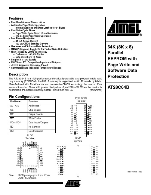
Features•Fast Read Access Time – 150 ns •Automatic Page Write Operation –Internal Address and Data Latches for 64 Bytes •Fast Write Cycle Times–Page Write Cycle Time: 10 ms Maximum –1 to 64-byte Page Write Operation •Low Power Dissipation –40 mA Active Current–100 µA CMOS Standby Current•Hardware and Software Data Protection•DATA Polling and Toggle Bit for End of Write Detection •High Reliability CMOS Technology –Endurance: 100,000 Cycles –Data Retention: 10 Years •Single 5V ± 10% Supply•CMOS and TTL Compatible Inputs and Outputs •JEDEC Approved Byte-wide Pinout•Commercial and Industrial Temperature RangesDescriptionThe AT28C64B is a high-performance electrically-erasable and programmable read only memory (EEPROM). Its 64K of memory is organized as 8,192 words by 8 bits.Manufactured with Atmel ’s advanced nonvolatile CMOS technology, the device offers access times to 150 ns with power dissipation of just 220 mW. When the device is deselected, the CMOS standby current is less than 100 µA.Pin ConfigurationsPin Name Function A0 - A12Addresses CE Chip Enable OE Output Enable WE Write Enable I/O0 - I/O7Data Inputs/Outputs NC No Connect DCDon ’t Connect PDIP , SOIC T op ViewTop ViewPLCC Top ViewNote:PLCC package pins 1 and 17 are DON ’T CONNECT.(continued)The AT28C64B is accessed like a Static RAM for the read or write cycle without the need for external components.The device contains a 64-byte page register to allow writing of up to 64 bytes simultaneously. During a write cycle, the addresses and 1 to 64 bytes of data are internally latched,freeing the address and data bus for other operations. Fol-lowing the initiation of a write cycle, the device will automat-ically write the latched data using an internal control timer.ING of I/O 7. Once the end of a write cycle has been detected, a new access for a read or write can begin.Atmel ’s AT28C64B has additional features to ensure high quality and manufacturability. The device utilizes internal error correction for extended endurance and improved data retention characteristics. An optional software data protec-tion mechanism is available to guard against inadvertent writes. The device also includes an extra 64 bytes of EEPROM for device identification or tracking.Block DiagramAbsolute Maximum Ratings*Temperature Under Bias................................-55°C to +125°C *NOTICE:Stresses beyond those listed under “Absolute Maximum Ratings ” may cause permanent dam-age to the device. This is a stress rating only and functional operation of the device at these or any other conditions beyond those indicated in the operational sections of this specification is not implied. Exposure to absolute maximum rating conditions for extended periods may affect device reliabilityStorage Temperature.....................................-65°C to +150°C All Input Voltages (including NC Pins)with Respect to Ground...................................-0.6V to +6.25V All Output Voltageswith Respect to Ground.............................-0.6V to V CC + 0.6V Voltage on OE and A9with Respect to Ground...................................-0.6V to +13.5VAT28C64B Device OperationREAD: The AT28C64B is accessed like a Static RAM. at the memory location determined by the address pins is asserted on the outputs. The outputs are put in the high-line control gives designers flexibility in preventing bus con-tention in their systems.BYTE WRITE: A low pulse on the WE or CE input with CE The address is latched on the falling edge of CE or WE, whichever occurs last. The data is latched by the first rising will automatically time itself to completion. Once a pro-gramming operation has been initiated and for the duration of t WC, a read operation will effectively be a polling operation.PAGE WRITE: The page write operation of the AT28C64B allows 1 to 64 bytes of data to be written into the device during a single internal programming period. A page write operation is initiated in the same manner as a byte write; after the first byte is written, it can then be followed by 1 to 63 additional bytes. Each successive byte must be loaded within 150µs (t BLC) of the previous byte. If the t BLC limit is exceeded, the AT28C64B will cease accepting data and commence the internal programming operation. All bytes during a page write operation must reside on the same page as defined by the state of the A6 to A12 inputs. For tion, A6 to A12 must be the same.The A0 to A5 inputs specify which bytes within the page are to be written. The bytes may be loaded in any order and may be altered within the same load period. Only bytes which are specified for writing will be written; unnecessary cycling of other bytes within the page does not occur. DATA POLLING: The AT28C64B features DATA Polling to indicate the end of a write cycle. During a byte or page write cycle an attempted read of the last byte written will result in the complement of the written data to be presented on I/O7. Once the write cycle has been completed, true data is valid on all outputs, and the next write cycle may begin. DATA Polling may begin at any time during the write cycle.TOGGLE BIT:provides another method for determining the end of a write cycle. During the write operation, successive attempts to read data from the device will result in I/O6 toggling between one and zero. Once the write has completed, I/O6 will stop toggling, and valid data will be read. Toggle bit reading may begin at any time during the write cycle.DATA PROTECTION: If precautions are not taken, inad-vertent writes may occur during transitions of the host sys-tem power supply. Atmel has incorporated both hardware and software features that will protect the memory against inadvertent writes.HARDWARE DATA PROTECTION: Hardware features protect against inadvertent writes to the AT28C64B in the following ways: (a) V CC sense – if V CC is below 3.8V (typi-cal), the write function is inhibited; (b) V CC power-on delay – once V CC has reached 3.8V, the device will automatically time out 5 ms (typical) before allowing a write; (c)write inhibit –inhibits write cycles; and (d) noise filter – pulses of less than 15 ns (typical) on the WE or CE inputs will not initiate a write cycle.SOFTWARE DATA PROTECTION: A software controlled data protection feature has been implemented on the AT28C64B. When enabled, the software data protection (SDP), will prevent inadvertent writes. The SDP feature may be enabled or disabled by the user; the AT28C64B is shipped from Atmel with SDP disabled.SDP is enabled by the user issuing a series of three write commands in which three specific bytes of data are written to three specific addresses (refer to the “Software Data Protection Algorithm” diagram in this datasheet). After writ-ing the 3-byte command sequence and waiting t WC, the entire AT28C64B will be protected against inadvertent writes. It should be noted that even after SDP is enabled, the user may still perform a byte or page write to the AT28C64B by preceding the data to be written by the same 3-byte command sequence used to enable SDP.Once set, SDP remains active unless the disable command sequence is issued. Power transitions do not disable SDP, and SDP protects the AT28C64B during power-up and power-down conditions. All command sequences must conform to the page write timing specifications. The data in the enable and disable command sequences is not actually written into the device; their addresses may still be written with user data in either a byte or page write operation. After setting SDP, any attempt to write to the device without the 3-byte command sequence will start the internal write timers. No data will be written to the device. However, for the duration of t WC, read operations will effectively be poll-ing operations.DEVICE IDENTIFICATION: An extra 64 bytes of EEPROM memory are available to the user for device identification. By raising A9 to 12V ± 0.5V and using address locations 1FC0H to 1FFFH, the additional bytes may be written to or read from in the same manner as the regular memory array.元器件交易网Notes:1.X can be V IL or V IH .2.Refer to the “AC Write Waveforms ” diagrams in this datasheet.3.V H = 12.0V ± 0.5V .DC and AC Operating RangeAT28C64B-15AT28C64B-20AT28C64B-25OperatingTemperature (Case)Com.0°C - 70°C 0°C - 70°C 0°C - 70°C Ind.-40°C - 85°C -40°C - 85°C -40°C - 85°C V CC Power Supply5V ± 10%5V ± 10%5V ± 10%Operating ModesMode CE OE WE I/O Read V IL V IL V IH D OUT Write (2)V IL V IH V IL D IN Standby/Write Inhibit V IH X (1)X High ZWrite Inhibit X X V IH Write Inhibit X V IL X Output Disable X V IH XHigh Z Chip Erase V ILV H (3)V IL High ZDC CharacteristicsSymbol Parameter ConditionMinMax Units I LI Input Load Current V IN = 0V to V CC + 1V 10µA I LO Output Leakage Current V I/O = 0V to V CC10µA I SB1V CC Standby Current CMOS CE = V CC - 0.3V to V CC + 1V Com., Ind.100µA I SB2V CC Standby Current TTL CE = 2.0V to V CC + 1V 2mA I CC V CC Active Current f = 5 MHz; I OUT = 0 mA40mA V IL Input Low Voltage 0.8V V IH Input High Voltage 2.0V V OL Output Low Voltage I OL = 2.1 mA 0.40V V OHOutput High VoltageI OH = -400 µA2.4V元器件交易网AT28C64BAC Read Waveforms (1)(2)(3)(4)Notes:1.ACC - t CE after the address transition without impact on t ACC .2.CE - t OE CE or by t ACC - t OE after an address changewithout impact on t ACC .3.t DF is specified from OE or CE whichever occurs first (C L = 5 pF).4.This parameter is characterized and is not 100% tested.Input Test Waveforms and Measurement LevelOutput Test LoadNote:1.This parameter is characterized and is not 100% tested.AC Read CharacteristicsSymbol ParameterAT28C64B-15AT28C64B-20AT28C64B-25Units MinMax MinMax MinMax t ACC Address to Output Delay 150200250ns t CE (1)CE to Output Delay 150200250ns t OE (2)OE to Output Delay 0700800100ns t DF (3)(4)CE or OE to Output Float 050055060ns t OHOutput Hold from OE, CE or Address, whichever occurred first00nsR F Pin Capacitancef = 1 MHz, T = 25°C (1)Symbol Typ Max Units Conditions C IN 46pF V IN = 0V C OUT 812pFV OUT = 0V元器件交易网AC Write WaveformsWE ControlledAC Write CharacteristicsSymbol ParameterMin MaxUnits t AS , t OES Address, OE Setup Time 0ns t AH Address Hold Time 50ns t CS Chip Select Setup Time 0ns t CH Chip Select Hold Time 0ns t WP Write Pulse Width (WE or CE)100ns t DS Data Setup Time 50ns t DH , t OEHData, OE Hold Timens元器件交易网AT28C64BPage Mode Write Waveforms (1)(2)Notes: 1.A6 through A12 must specify the same page address during each high to low transition of WE (or CE).2.OE must be high only when WE and CE are both low.Chip Erase Waveformst S = t H = 1 µsec (min.)t W = 10 msec (min.)V H = 12.0 ± 0.5VPage Mode CharacteristicsSymbol Parameter MinMax Units t WC Write Cycle Time10ms t WC Write Cycle Time (option available; contact Atmel sales office for ordering part number)02ms t AS Address Setup Time 0ns t AH Address Hold Time 50ns t DS Data Setup Time 50ns t DH Data Hold Time 0ns t WP Write Pulse Width 100ns t BLC Byte Load Cycle Time 150µs t WPHWrite Pulse Width High50ns元器件交易网Software Data Protection Enable Algorithm (1)Notes for software program code:1.Data Format: I/O7 - I/O0 (Hex);Address Format: A12 - A0 (Hex).2.Write Protect state will be activated at end ofwrite even if no other data is loaded.3.Write Protect state will be deactivated at end ofwrite period even if no other data is loaded.4. 1 to 64 bytes of data are loaded.Software Data Protection Disable Algorithm (1)Software Protected Write Cycle Waveforms (1)(2)Notes: 1.A6 through A12 must specify the same page address during each high to low transition of WE (or CE) after the software code has been entered.2.元器件交易网AT28C64BNotes:1.These parameters are characterized and not 100% tested.2.See “AC Read Characteristics ”.Notes:1.These parameters are characterized and not 100% tested.2.See “AC Read Characteristics ”.Toggle Bit Waveforms (1)(2)(3)Notes: 1.2.Beginning and ending state of I/O6 will vary.3.Any address location may be used but the address should not vary.Data Polling Characteristics (1)Symbol Parameter Min TypMaxUnits t DH Data Hold Time 0ns t OEH OE Hold Time 0ns t OE OE to Output Delay (2)ns t WR Write Recovery TimensToggle Bit Characteristics (1)Symbol Parameter Min TypMaxUnits t DH Data Hold Time 10ns t OEH OE Hold Time 10ns t OE OE to Output Delay (2)ns t OEHP OE High Pulse 150ns t WR Write Recovery Time0ns元器件交易网元器件交易网AT28C64BNote:1.See “Valid Part Numbers ” table below.Ordering Information (1)t ACC (ns)I CC (mA)Ordering Code Package Operation Range Active Standby 150400.1A T28C64B-15JC A T28C64B-15PC A T28C64B-15SC A T28C64B-15TC 32J 28P628S 28T Commercial (0°C to 70°C)A T28C64B-15JI A T28C64B-15PI A T28C64B-15SI A T28C64B-15TI32J 28P628S 28T Industrial (-40°C to 85°C)200400.1A T28C64B-20JC A T28C64B-20PC A T28C64B-20SC A T28C64B-20TC 32J 28P628S 28T Commercial (0°C to 70°C)A T28C64B-20JI A T28C64B-20PI A T28C64B-20SI A T28C64B-20TI32J 28P628S 28T Industrial (-40°C to 85°C)250400.1A T28C64B-25JC A T28C64B-25PC A T28C64B-25SC A T28C64B-25TC 32J 28P628S 28T Commercial (0°C to 70°C)A T28C64B-25JI A T28C64B-25PI A T28C64B-25SI A T28C64B-25TI32J 28P628S 28TIndustrial (-40°C to 85°C)Valid Part NumbersThe following table lists standard Atmel products that can be ordered.Device Numbers Speed Package and Temperature Combinations AT28C64B 15JC, JI, PC, PI, SC, SI, TC, TI AT28C64B 20JC, JI, PC, PI, SC, SI, TC, TI AT28C64B 25JC, JI, PC, PI, SC, SI, TC, TI AT28C64B–WDie ProductsReference Section: Parallel EEPROM Die Products元器件交易网AT28C64B12Packaging Information© Atmel Corporation 1999.Atmel Corporation makes no warranty for the use of its products, other than those expressly contained in the Company ’s standard war-ranty which is detailed in Atmel ’s Terms and Conditions located on the Company ’s web site. The Company assumes no responsibility for any errors which may appear in this document, reserves the right to change devices or specifications detailed herein at any time without notice, and does not make any commitment to update the information contained herein. No licenses to patents or other intellectual prop-erty of Atmel are granted by the Company in connection with the sale of Atmel products, expressly or by implication. Atmel ’s products are not authorized for use as critical components in life support devices or systems.Marks bearing ® and/or ™ are registered trademarks and trademarks of Atmel Corporation.Terms and product names in this document may be trademarks of others.Atmel HeadquartersAtmel OperationsCorporate Headquarters2325 Orchard Parkway San Jose, CA 95131TEL (408) 441-0311FAX (408) 487-2600EuropeAtmel U.K., Ltd.Coliseum Business Centre Riverside WayCamberley, Surrey GU15 3YL EnglandTEL (44) 1276-686-677FAX (44) 1276-686-697AsiaAtmel Asia, Ltd.Room 1219Chinachem Golden Plaza 77 Mody Road Tsimhatsui East Kowloon Hong KongTEL (852) 2721-9778FAX (852) 2722-1369JapanAtmel Japan K.K.9F, Tonetsu Shinkawa Bldg.1-24-8 ShinkawaChuo-ku, Tokyo 104-0033JapanTEL (81) 3-3523-3551FAX (81) 3-3523-7581Atmel Colorado Springs1150 E. Cheyenne Mtn. Blvd.Colorado Springs, CO 80906TEL (719) 576-3300FAX (719) 540-1759Atmel RoussetZone Industrielle13106 Rousset Cedex FranceTEL (33) 4-4253-6000FAX (33) 4-4253-6001Fax-on-DemandNorth America:1-(800) 292-8635International:1-(408) 441-0732e-mailliterature@Web Site BBS1-(408) 436-43090270H –12/99/xM。
AT28C64中文资料

AT28C64B 64Kbit,并行EEPROMs 存储器AT28C64B 器件操作(1)ATMEL 爱特梅尔AT28C64B 程序存储器芯片读操作ATMEL 爱特梅尔AT28C64B 程序存储器芯片读操作访问就像使用静态RAM 一样,当CE 和OE 为低电平,WE 为高电平,由地址引脚上电平决定的存储单元中的存储的数据就被读出。
无论何时CE 或OE 为高电平时,AT28C64B 输出引脚上都呈高阻状态。
AT28C64B 这种双信号控制机制给设计者防止总线冲突带来灵活性。
(2)ATMEL 爱特梅尔AT28C64B 程序存储器芯片后备状态CE 信号是芯片选择控制信号,实际上同时也作为电源控制信号。
当其为高电平时,ATMEL 爱特梅尔AT28C64B 程序存储器芯片就进入低功耗后备状态。
这时ATMEL 爱特梅尔AT28C64B 程序存储器芯片输出呈高阻状态,并与OE 信号无关。
(3)ATMEL 爱特梅尔AT28C64B 程序存储器芯片数据保护为了确保数据的完整性和安全性,持别是在上电和掉电过渡过程中,可以用以下方法实现数据保护:①利用内部检测电路对电源电压Vcc 进行检测,当ATMEL 爱特梅尔AT28C64B 程序存储器芯片检测到的电压低于规定的阂值时,AT28C64B 就禁止内部非易失性编程操作的初姑化。
当达到阂值电压时,AT28C64B 芯片在允许字节写入之前将自动输出5阳的定时脉冲。
②ATMEL 爱特梅尔AT28C64B 程序存储器芯片片内有一个丽信号滤波电路,可以防止而信号负脉冲从初姑化到写入周期所持续的时间小于10ns。
③ATMEL爱特梅尔AT28C64B程序存储器芯片在上电和掉电期间,通过保持WE或CE 为高电平,或者OE为低电乎都可以封锁字节写入周期。
(4)ATMEL爱特梅尔AT28C64B程序存储器芯片写操作把数据写入AT28C64B芯片类似于静态RAM的操作,当OE为高电平、WE或CE为低电平时,相对应的CE或WE信号为低电平,就对字节写入操作进行韧始化。
平板电脑主流芯片

平板电脑主流芯片目前平板大部分主控芯片是使用ARM内核,少数是MIPS内核。
比如君正4760,主频为600MHz,就是采用MIPS架构。
另外还有使用Atom芯片的平板电脑。
ARM9系列威盛WM8505/WM8505+65nm工艺ARM926E 300MHz/400MHz,Linpack 1-1.25MFlops(1.6系统)RAM: 128M DDR2,16bit只有个JPEG硬解,视频支持很弱,无3D加速代表机型:国美飞触1代,山寨VIA平板性能★☆☆☆☆视频★☆☆☆☆---------------------------------------------------瑞芯微RK280865nm工艺ARM926E 600MHz,Linpack 2-2.5MFlops(1.5系统)RAM: 128M SDRAM,32bit视频子系统:Ceva MM2000,基于550MHz的DSP多格式,RV,H.264,VC-1,H.263,MPEG4最高720p,流畅576p,无3D加速代表机型:蓝魔W7,爱可视7HT,山寨apad等性能★★☆☆☆视频★★★☆☆瑞芯微RK281865nm工艺ARM926E 660MHz,Linpack 3MFlops+(2.1系统)RAM: 256M DDR2,32bit视频子系统:Ceva MM2000,基于600MHz的DSP多格式,RV,H.264,VC-1,H.263,MPEG4最高720p代表机型:蓝魔W9,W11,原道N6性能★★★☆☆视频★★★☆☆ARM11Telechips TCC890265nm工艺ARM1176JZF-S 540MHz/720MHz,Linpack 2.3/3.5MFlops(2.1系统)RAM: 256M DDR2,32bit视频子系统:ARM Mali-VE6,基于硬解多格式,RV,H.264,VC-1,H.263,MPEG4最高1080p,1080p流畅3D加速: ARM Mali-200代表机型:智器V系列,一些山寨平板性能★★★☆☆视频★★★★★三星S3C641065nm工艺ARM1176JZF-S 666MHz/800MHz,Linpack ~3.5MFlops(2.1系统)RAM: 128M DDR/256M mDDR,32bit视频子系统:三星,硬件解码支持720×480下的H.264 BP3D加速:三星自有代表机型:智器Q系列,魅族M8,三星i5700性能★★★☆☆视频★☆☆☆☆盈方微IMAPX20065nm工艺ARM1176JZF-S 1GHz,Linpack ~9.8MFlops(2.1系统开启JIT,不开估计在4-4.5)RAM: 256M DDR2,32bit视频子系统:On2 Hantro 8190,硬件解码多格式,RV,H.264,VC-1,H.263,MPEG4,VP6最高1080p3D加速:有代表机型:卓尼斯epad,国美飞触2代性能★★★☆☆视频★★★★☆高通MSM720165nm工艺ARM1136J-S 528MHz,Linpack ~2-2.5MFlops(1.6系统)RAM: 128/256M mDDR,32bit视频子系统:高通QDSP5000支持720×480以下H.264 BP3D加速: Adreno 130代表机型:G1 G2 G3之类的性能★★☆☆☆视频★☆☆☆☆Cortex-A8高通QSD8x5065nm工艺Scorpion 1GHz,Linpack 7-7.5MFlops(2.1系统)RAM: 256/512M mDDR,32bit视频子系统:高通QDSP6000支持720p H.264,但一般只有480p H.264流畅(BP或者MP) 通过软件解码能勉强支持480p多格式流畅3D加速: Adreno 200(AMD Z430)代表机型:google N1, Dell streak性能★★★★★视频★★☆☆☆德州仪器OMAP3430/353065nm工艺Cortex-A8 550/720MHz,Linpack ~4.5(550MHz)/5.9(800MHz)(2.1系统)RAM: 256M mDDR,32bit视频子系统:IVA2+,基于C64x+ DSP,430MHz多格式,但除去爱可视,很多厂商都没做解码通过软件解码,配合超频,能勉强支持480p多格式流畅3D加速: PowerVR SGX530代表机型:moto milestone,爱可视5,维智A81性能★★★★☆视频★★☆☆☆三星S5PC10065nm工艺Cortex-A8 667/800MHzRAM: 256M mDDR,32bit视频子系统:PowerVR VXD370多格式,H.264,VC-1,MPEG4最高1080p 3D加速: PowerVR SGX535代表机型:touch3,3GS性能★★★★☆视频★★☆☆☆(苹果)飞思卡尔i.MX51565nm工艺Cortex-A8 800MHz/1GHzRAM: 256/512M DDR2,32bit视频子系统:硬解多格式,H.264,VC-1,MPEG4,RV最高720p通过软件解码能勉强支持480p多格式流畅3D加速: Adreno 200(AMD Z430)代表机型:viliv P3性能★★★★★视频★★★★☆三星S5PC110/S5PV21045nm工艺优化的Cortex-A8 800MHz/1GHz,512K L2,Linpack 8-8.5(1GHz)(2.1系统)RAM: 512M mDDR2,32bit视频子系统:PowerVR VXD370多格式,H.264,VC-1,MPEG4最高1080p通过软件解码能勉强支持480p多格式流畅3D加速: PowerVR SGX540代表机型:三星i9000,Galaxy Tab采用类似的A4芯片的有iPad、iPod touch4、iPhone 4性能★★★★★★视频★★★★☆德州仪器OMAP3630/364045nm工艺Cortex-A8 800MHz/1GHzRAM: 512M mDDR2,32bit视频子系统:IVA2+,基于C64x+ DSP,430MHz多格式,但除去爱可视,很多厂商都没做解码通过软件解码能勉强支持480p多格式流畅3D加速: PowerVR SGX530代表机型:moto droidx,droid2,爱可视新发布的那一串机器性能★★★★★视频★★☆☆☆Cortex-A9NVidia Tegra240nm工艺(TMSC)Cortex-A9 1GHz双核 + VFPRAM: 512M/1G DDR2,32bit视频子系统:硬件解码多格式,H.264,VC-1,MPEG4最高1080p3D加速: GeForce ULV代表机型:微星Harmony,万利达Zpad、东芝Folio性能★★★★★★★★★★视频★★★★☆德州仪器OMAP4430/444045nm工艺Cortex-A9 1GHz/1.3GHz双核 + NeonRAM: 512M/1G+ DDR3,64bit视频子系统:IVA3,高清硬件解码单元 + C64x+ Lite DSP多格式1080p,DSP部分提供可编程性3D加速: PowerVR SGX540代表机型:性能★★★★★★★★★★★★视频★★★★☆+Amlogic(晶晨)AML8726-M( Cortex A9 +1080P +3D GPU)日本RENESASARM CORTEX A9,双CPU(533*2)+GPU,支持1080P,3D图形加速,Flash 10.1 NEC意法半导体(由意大利的SGS微电子公司和法国Thomson半导体公司合并而成)。
- 1、下载文档前请自行甄别文档内容的完整性,平台不提供额外的编辑、内容补充、找答案等附加服务。
- 2、"仅部分预览"的文档,不可在线预览部分如存在完整性等问题,可反馈申请退款(可完整预览的文档不适用该条件!)。
- 3、如文档侵犯您的权益,请联系客服反馈,我们会尽快为您处理(人工客服工作时间:9:00-18:30)。
FUNCTIONAL BLOCK DIAGRAM
DIP (C5-1)
L1C51C9B (L6)
Document # EEPROM101 REV B Revised July 2007
1
元器件交易网
PYX28C64
MAXIMUM RATINGS(1)
10
10
tOHQZ Output Disable to Output in High Z
80
80
tAVQX Output Hold from Address Change
0
0
tPU Chip Enable to Power Up Time
250
250
tPD Chip Disable to Power Down Time
___
60
mA
Notes:
1. Stresses greater than those listed under MAXIMUM RATINGS may cause permanent damage to the device. This is a stress rating only and functional operation of the device at these or any other conditions above those indicated in the operational sections of this specification is not implied. Exposure to MAXIMUM rating conditions for extended periods may affect reliability.
tEHWH CE Hold Time
tWHOH OE Hold Time
tOHAV Erase Time
tWLWH2 Chip Erase Time
VH High Voltage for Chip Clear
-200 Min Max
10
20
150
0 0 20 20 150
50
10
0.2 2 1 1 1 1 200 150 12 13
元器件交易网
PYX28C64 8K x 8 EEPROM
FEATURES
Access Times of 200, 250, 300 and 350 ns
Single 5V±10% Power Supply
Simple Byte and Page Write
Low Power CMOS: - 60 mA Active Current - 200 µA Standby Current
OH (TTLLoad)
I = –4 mA, V = Min.
OH
CC
2.4
V
ILI Input Leakage Current
ILO Output Leakage Current
ISB
Standby Power Supply Current (TTL Input Levels)
VCC = Max.
VCC = 5.0V, TA = 25°C, f = 1.0MHz
Symbol Parameter Conditions Typ. Unit
C IN
COUT
Input Capacitance VIN = 0V 10 pF Output Capacitance VOUT = 0V 10 pF
DC ELECTRICAL CHARACTERISTICS
Over recommended operating temperature and supply voltage(2)
Symbol
Parameter
Test Conditions
VIH Input High Voltage
VIL Input Low Voltage
VHC CMOS Input High Voltage VLC CMOS Input Low Voltage
50
50
-300 Min Max 300
300 300 100 10 80 10 80 0 250 50
-350
Unit
Min Max
350
ns
350 ns
350 ns
100 ns
10
ns
80 ns
10
ns
80 n
50 ns
TIMING WAVEFORM OF READ CYCLE
V = GND to V
IN
CC
VCC = Max., CE = VIH,
V = GND to V
OUT
CC
CE ≥ VIH, OE = VIL, V = Max,
CC
f = Max., Outputs Open
–10
+10
µA
–10
+10
µA
___
3
mA
Standby Power Supply ISB1 Current
Fast Write Cycle Times
DESCRIPTION
The PYX28C64 is a 5 Volt 8Kx8 EEPROM using floating gate CMOS Technology. The device supports 64-byte page write operation. The PYX28C64 features DATA and Toggle Bit Polling as well as a system software scheme used to indicate early completion of a Write Cycle. The device also includes user-optional software data protection. Endurance is 10,000 or 100,000 Cycles and Data Retention is 100 Years. The device is available in a 32-Pin LCC package as well as a 28-Pin 600 mil wide Ceramic DIP.
PYX28C64
TIMING WAVEFORM OF BYTE WRITE CYCLE (WE CONTROLLED)
200
250
tOLQV Output Enable Access Time
100
100
tELQX Chip Enable to Output in Low Z
10
10
tEHQZ Chip Disable to Output in High Z
80
80
tOLQX Output Enable to Output in Low Z
(CMOS Input Levels)
CE ≥ VHC, VCC= Max, f = 0, Outputs Open
VIN ≤ VLC or VIN ≥ VHC
___
250
µA
I
Supply Current
CC
CE = OE = VIL, WE = VIH, All I/O's = Open,
Inputs = VCC = 5.5V
tWHWL1 Write Cycle Time tEHEL1
tAVEL Address Setup Time tAVWL
tELAX tWLAX
Address Hold Time
tWLEL tELWL
Write Setup Time
tWHEH Write Hold Time
tOHEL tOHWL
OE Setup Time
–65 to +150 °C
1.0
W
50
mA
RECOMMENDED OPERATING TEMPERATURE AND SUPPLY VOLTAGE
Grade(2) Military
Ambient Temperature
–55°C to +125°C
GND 0V
VCC 5.0V ± 10%
CAPACITANCES(4)
150
ns
0
ns
0
ns
20
ns
20
ns
150
ns
50
ns
10
ns
0.2 2 µs
1
µs
1
µs
1
µs
1
µs
200
ms
150
ns
12 13 V
Document # EEPROM101 REV B
Page 4 of 11
元器件交易网 TIMING WAVEFORM OF BYTE WRITE CYCLE (CE CONTROLLED)
-250 Min Max
10
20
150
0 0 20 20 150
50
10
0.2 2 1 1 1 1 200 150 12 13
-300 Min Max
10
20
150
0 0 20 20 150
50
10
0.2 2 1 1 1 1 200 150 12 13
-350
Unit
Min Max
10 ms
20
ns
Software Data Protection Fully TTL Compatible Inputs and Outputs Endurance: 10,000 or 100,000 Cycles Data Retention: 100 Years Available in the following Packages: – 32-Pin Ceramic LCC (450 x 550 mils) – 28-Pin 600 mil Ceramic DIP