TDK贴片电容型号选型规格书
TDK电容清单

SMD,一般
C0603CH1H1R5C
C
SMD,中耐压
C1608CH2E101J
C
SMD,高耐压,COG
C4532CH3F101K
C
SMD,高耐压,X7R
C4520X7R3D471K
C
SMD,低ESL,倒装型(LW倒装)
C0816JB1C103K
C
SMD,高温保证
C11608X8R2A102K
CC45
圆板型带导线,光高频率低损耗
CD
圆板型带导线,安规品
CD(S)70-B2GA101KYNS
CK45
圆板型带导线,一般
CK45-B3FD101KYNN
CK45-RB
圆板型带导线,光高频率低损耗
CK45-B3DD101KYNR
CK45-RR
圆板型带导线,光高频率低损耗
CK45-R3DD101K-NR
CKC
SMD阵列,4单元
CKCL44CH1H100F
CKC
SMD阵列,2单元
CKCM25CH1H100F
CKD
SMD,低ESL,3端贯通
CKD510JB1H220S
CKG
SMD金属支架电容
CKG57NX5R1H226M
CLL
SMD,低ESL,ULI
CLLD11X7R1A104M
CS
圆板型带金属端子,安规品
TDK电容清单
系列号
型号举例
备注
C
SMD,薄型
C1608JB1H104K
左边的型号只是随便举个例子,我们有各种尺寸、电容、温度的型号,只要您需要TDK的东西都可以和我们联系。
ROHM的产品我们有电容、二极管、IC等,IC包括电源木块,升压和降压、打印头等。
通用型贴片电容规格书(选型手册)

【 南京南山半导体有限公司 — 贴片电容选型资料】MULTILAYER CHIP CERAMIC CAPACITORCOG/COHCOG, ,-55125,030ppm/060ppm/0805CG101J500NT(PF) ( 0402 0.04 0603 0.06 0805 0.08 1206 0.12 ) 0.02 0.03 0.05 0.06 1.00 1.60 2.00 3.20 ( ) 0.50 0.80 1.25 1.60 CG CH COG NPO COH 100 101 102 10 100 1J G C B D5.00% 2.00% 0.25PF 0.10PF 0.50PF10 10 10 1026R3 100 250 5006.3V 10V 25V 50VS C N / / T BWBWTL mm L 0402 0603 0805 1206 1005 1608 2012 3216 1.00 1.60 2.00 3.20 0.05 0.10 0.20 0.30 W 0.50 0.80 1.25 1.60 0.05 0.50 0.10 0.80 0.20 0.80 1.00 1.25 0.20 0.80 1.00 1.25 T WB 0.05 0.25 0.10 0.30 0.20 0.50 0.20 0.20 0.20 0.60 0.20 0.20 0.10 0.10 0.20 0.3015【 南京南山半导体有限公司 — 贴片电容选型资料】0.80 0.20 1.00 0.20 0.50 0.80 0.20 1.00 0.20 0.600.20 0.30【 南京南山半导体有限公司 — 贴片电容选型资料】MULTILAYER CHIP CERAMIC CAPACITORCOG/COH 0402 0603 0805 12066.3V 10V 16V 25V 50V 6.3V 10V 16V 25V 50V 6.3V 10V 16V 25V 50V 6.3V 10V 16V 25V 50V0.5PF 1PF 2PF 3PF 4PF 5PF 6PF 7PF 10PF 22PF 33PF 47PF 68PF 100PF 120PF 150PF 180PF 220PF 330PF 470PF 560PF 680PF 1000PF 2200PF 2700PF 3300PF 4700PF 5600PF 6800PF 10nF 12nF 15nF 22nF 47nF 68nF 100nF17【 南京南山半导体有限公司 — 贴片电容选型资料】04020603080512066.3V 10V 16V 25V 50V 6.3V 10V 16V 25V 50V 6.3V 10V 16V 25V 50V 6.3V 10V 16V 25V 50VCapacitance0.5PF 1PF 2PF 3PF 4PF 5PF 6PF 7PF 10PF 22PF 33PF 47PF 68PF 100PF 120PF 150PF 180PF 220PF 330PF 470PF 560PF 680PF 1000PF 2200PF 2700PF 3300PF 4700PF 5600PF 6800PF 10nF 12nF 15nF 22nF 47nF 68nF 100nF【 南京南山半导体有限公司 — 贴片电容选型资料】MULTILAYER CHIP CERAMIC CAPACITORCOG COHPH~SLCOG PH SH SL TH RH UJCOH1-55125-55851. 2. 3. 2 4. 5. , , , , , 103 4 Cr 5PF 0.56% -4 5PF Cr 50PF 1.5 [(150/Cr)+7] 10 Cr 50PF 0.15% C C 10nF Ri 10nF Ri 5 10 Cr 500s 3 50mA 150+0/-10 8 25 9 75 235 5 2 0.5 25 60 265 10 1 25 : 1 2 100 170 120 200 1 1 2.5mm/ 24 2 5 5 5 2.5mm/ 245 24 -55 125 2 -55 85 60 510:HP4278A 1. 2. 3. (D.F.) :1.0 C : : (HP4284 25 5 0.2V 0.1MHz; 0.1KHZ ) 1000PF,1.0 :SF2511 , 60 60 1 5 :30% 75%5:C<1000PF,1.06I.R.7>3x150+0/-10 5% 0.5PF D.F. 10 I.R. 24 245【 南京南山半导体有限公司 — 贴片电容选型资料】General COGCOHPHSL MLCC reliability test methodStandard Number Item COG COH MLCC for General-use -55 125 PH, RH, SH, TH, UJ, SL MLCC for General-use -55 85 Check by using microscope 10 . Test Method1Operating Temperature RangeAppearance21.Good ceramic body color continuity. 2.The chips have no visual damages and must be very smooth. 3.No exposed inner- electrode, no cracks or holes. 4.The outer electrode should have no cracks, holes, damages or surface oxidation. 5.Outer electrode no prolongation or the prolongation is less than half of that of the termination width.3 4 5Dimensions Capacitance Dissipation Factor (DF)Within the specified dimensions Within the specified tolerance Cr 5PF 0.56% 5PF Cr 50PF 1.5 [(150/Cr)+7] 10-4 Cr 50PF 0.15% C C 10nF Ri 10nF Ri 5 1010 Cr 500sUsing micrometer or vernier calipers Measuring Equipments:HP4278 capacitance meter,HP4284 capacitance, Measuring Conditions: 1.Measuring Temperature:25 5 .Humidity: 30% 75%. 2.Measuring Voltage:1.0 0.2V. 3.Measuring Frequency:C<1000PF 1.0 0.1MHz C 1000PF 1.0 0.1KHz Measuring Equipment:Insulation resistance meter (such as Sf2511 insulation resistance). Measuring Method:Must measure at rated voltage, and measure the IR within 60 5 seconds. Must measure at 3 times rated voltage, dwell time: 60 1 seconds, no short and the changing/discharging current less than 50mA. First, pre-heat: heat treat 60 5 minutes at 150+0/-10 , then set it for 24 2 hours at room temperature. Measure the capacitance at -55 125 or -55 85 , the capacitance change ratio comparing to that of 25 must be within the specified range. Dip the capacitor into ethanol or colophony solution, and then dip it into 235 5 ( or 245 5 leadless eutedtic solder solution ) eutectic solder solution hanving lead for 2 0.5 seconds. Dipping speed: 25 2.5mm/second. First pre-heat: heat treat for 60 5 minutes at 150+0/-10 , then set it for 24 2 hours at room temperature. Then pre-heat the capacitance according to the following chart. Dip the capacitor into 265 5 eutectic solder solution for 10 1 seconds. Then set it for 24 2 hours at room temperature, then measure. Dipping speed: 25 2.5mm/second. Preheat conditions: Stage 1 2 Temperature 100 170 120 200 Time 1minute 1minute6Insulation Resistance7Withstanding Voltage Capacitance Temperature Characteristic>3x rated continuous working voltage Must meet the capacitor character temperature coefficient requirements within the operating temperature range. Tin coverage should be 75% of the outer electrode Appearance Cap. Change ratio DF No defects visible 5%or 0.5PF (whichever is larger)89SolderabilityResistance to Soldering10Same as original spec Same as original specIR46【 南京南山半导体有限公司 — 贴片电容选型资料】MULTILAYER CHIP CERAMIC CAPACITOR1 10N11 10N,10 1 :1.0mm/ 11.5mm 10 D.F. 12 55Hz 210 55Hz 10Hz 6 123 420 mm mmmm13mmmmmmmm150+0/-10 14 24 2 24 260 547【 南京南山半导体有限公司 — 贴片电容选型资料】NumberItems Adhesive Strength of TerminationStandard No removal of the terminations or other defect shall occurTest Method Solder the capacitor to the test jig (glass epoxy resin board) shown in Fig.1 using a eutectic solder.Then apply a 10N force inthe direction shown as the arrowhead.The aoldering shall be done either with an iron or using the reflow method and shall be conducted with care so that an iron or using the refow method and shall be conducted with care so that the soldering is uniform and free of defects such as heat shock,etc. 10N,10 1s Speed:1.0mm/s Glss epoxy resinboard11Fig.1 Vibration Resistance Appearance Capacitance No defects or abnormities Within the specified tolerance range Same as original spec12DFSolder the capacitor to the test jig (glass epoxy resin board). The capacitor should be subjected to a simple harmonic motion having a total amplitude of 1.5mm, the frequency being varied uniformly between the approximate limits of 10 and 55Hz, shall be traversed (from 10 Hz to 55 Hz then 10 Hz again) in approximately 1 minute.This motion shall be applied for a period of 2 hours in each 3 mutually perpendicular directions (total is 6 hours).Same i standarFif.2 Bending Resistance No cracks or other defects shall occur Solder the capacitor to the test jig (glass epoxy resin board) shown in Fig.3 using a eutectic solder. Then apply a 10N force in the direction shown as Fig.4. The soldering shall be done either with an iron or using the reflow method and shall be conducted with care so that the soldering is uniform and free of defects such as mm heat shock, etc.mm13mm mm mm14Temperature CycleAppearance No defects or abnormitiesPre-treatment: Heat-treat the capacitor for 60 5minutes at 150+0/-10 , then set it for 24 2 hours at room temperature. Perform five cycles according to the four heat treatments listed in the following table. Set it for 24 2 hours at room temperature, then measure.48mm【 南京南山半导体有限公司 — 贴片电容选型资料】MULTILAYER CHIP CERAMIC CAPACITOR2.5% 0.25PF, 1 10000M 2 3 4 2 3 30 3 2 3 30 3 2 314D.F. I.R.40 290 95 24 2500+24/-05% 0.5PF, 15 ( ) D.F. I.R. 10000M40 2 500+24/-0 5% 0.5PF, 16 D.F. I.R. 10000M90 95 24 22 50mA 5% 0.5PF, 17 D.F. I.R. 10000M1000 12 24 249【 南京南山半导体有限公司 — 贴片电容选型资料】NumberItem Temperature CycleStandard Cap. Change ratio D.F. I.R. 2.5% or 0.25 PF (whichever is larger) Same as original spec More than 10000M Heat-treatment:Test Method14stage temperature 1 lowest opeating temperature 3 2 normal temperature 3 high operating temperature 2 4 normal temperaturetime min. 30 3 2 3 30 3 2 3Humidity Steady StateAppearance Cap. Change ratio D.F. I.R.No defects or abnormities 5% or 0.5 PF (whichever is larger) Same as original spec More than 10000MSet the capacitor for 500+24/-0 hours at the condition of 40 2 and 90-95% humidity. Then remove and set it for 24 2 hours at room temperature, then measure.15Humidity LoadAppearance Cap. Change ratioNo defects or abnormities 5% or 0.5 PF (whichever is larger) Same as original spec More than 10000MApply rated voltage to the capacitor for 500+24/-0 hours at the condition of 40 2 and 90-95% humidity. Remove and set it for 24 2 hours at room temperature, then measure.16D.F. I.R.Life TestAppearance Cap. Change ratioNo defects or abnormities 5% or 0.5 PF (whichever is larger) Same as original spec More than 10000MApply two times rated voltage to the capacitor for 1000 12 hours at the upper temperature limits, the charging current should be less than 50mA. Remove and set it for 24 2 hours at room temperature, then measure.17D.F. I.R.5057-10%-5%0%5%10%COG 50VX7R 50V Z5U 50V Y5V50V010********-100%-80%-60%-40%-20%0%20%40%[Vdc]COG :1MHZ X7R,Z5U,Y5V:1KHZZ5U 50VY5V 50V X7R 50VC0G 50V0123-20%0%+20%+40%+60%^+80%COG PH RH SH TH UHCOG X7R Y5V,Z5U05010010001000010%0%-10%-20%-30%-40%[Hr]X7R20%0%[Vr ms ]COG :1MHZ X7R,Z5U,Y5V:1KHZMULTILAYER CHIP CERAMIC CAPACITOR58-5%0%5%10%-100%-80%-60%-40%-20%0%20%40%Z5U 50VY5V 50V X7R 50VC0G 50V0123-20%0%+20%+40%+60%^+80%COG X7R Y5V,Z5U05010010001000010%0%-10%-20%-30%-40%0%GENEREL-USE MLCC CHARCCTER PROFILESCapacitance change ratio DC Voltage[Vdc]Measuring condition COG :1MHzX7R,Z5U,Y5V:1KHzCOG and PHRH SH TH UH siriestemperature coefficentDC Capacitance-AC VoltageCharactericsCapacitance change_agingTime[Hr]X7R tempreture characteristicsZ5U [Vr ms ]Capacitance change ratioCapacitance change ratio Capacitance change ratio Capacitance change ratio。
TDK车规车载级贴片电容CGA4型号大全
系列:车载用MPQ(最小包装):3,000pcs 包装规则:φ180mm压纹带应用:汽车电子,AEC-Q200 CGA4系列TDK常用规格如下:CGA4J3X7R1Hvalue="474" unitname="m" w:st="on">474M125AB CGA4J3X7R1Hvalue="474" unitname="m" w:st="on">474M125AECGA4J3X7R1H684K125ABCGA4J3X7R1Hvalue="684" unitname="m" w:st="on">684M125ABCGA4J3X7R1V105K125ABCGA4J3X7R1Vvalue="105" unitname="m" w:st="on">105M125ABCGA4J3X7R1V474K125ABCGA4J3X7R1Vvalue="474" unitname="m" w:st="on">474M125ABCGA4J3X7R1V684K125ABCGA4J3X7R1Vvalue="684" unitname="m" w:st="on">684M125ABCGA4J3X7R2E103K125AACGA4J3X7R2E103K125AECGA4J3X7R2Evalue="103" unitname="m" w:st="on">103M125AA CGA4J3X7R2Evalue="103" unitname="m" w:st="on">103M125AE CGA4J3X7R2E153K125AACGA4J3X7R2Evalue="153" unitname="m" w:st="on">153M125AA CGA4J3X7R2E223K125AACGA4J3X7R2E223K125AECGA4J3X7R2Evalue="223" unitname="m" w:st="on">223M125AA CGA4J3X7R2Evalue="223" unitname="m" w:st="on">223M125AE CGA4J3X7R2E682K125AACGA4J3X7R2Evalue="682" unitname="m" w:st="on">682M125AACGA4J3X7Svalue="1" unitname="a" w:st="on">1A106K125ABCGA4J3X7Svalue="1" unitname="a" w:st="on">1Avalue="106" unitname="m" w:st="on">106M125ABCGA4J3X7Svalue="1" unitname="a" w:st="on">1A685K125ABCGA4J3X7Svalue="1" unitname="a" w:st="on">1Avalue="685" unitname="m" w:st="on">685M125ABCGA4J3X8R1E474K125ABCGA4J3X8R1E474K125ADCGA4J3X8R1Evalue="474" unitname="m" w:st="on">474M125ABCGA4J3X8R1Evalue="474" unitname="m" w:st="on">474M125ADCGA4J3X8R1H154K125ABCGA4J3X8R1H154K125ADCGA4J3X8R1Hvalue="154" unitname="m" w:st="on">154M125ABCGA4J3X8R1Hvalue="154" unitname="m" w:st="on">154M125ADCGA4J3X8R1H224K125ABCGA4J3X8R1H224K125ADCGA4J3X8R1Hvalue="224" unitname="m" w:st="on">224M125ABCGA4J3X8R1Hvalue="224" unitname="m" w:st="on">224M125ADCGA4J3X8Rvalue="2" unitname="a" w:st="on">2A333K125ABCGA4J3X8Rvalue="2" unitname="a" w:st="on">2A333K125ADCGA4J3X8Rvalue="2" unitname="a" w:st="on">2Avalue="333" unitname="m" w:st="on">333M125ABCGA4J3X8Rvalue="2" unitname="a" w:st="on">2Avalue="333" unitname="m" w:st="on">333M125ADCGA4J3X8Rvalue="2" unitname="a" w:st="on">2A473K125ABCGA4J3X8Rvalue="2" unitname="a" w:st="on">2A473K125ADw:st="on">473M125ABCGA4J3X8Rvalue="2" unitname="a" w:st="on">2Avalue="473" unitname="m" w:st="on">473M125ADCGA4J3X8Rvalue="2" unitname="a" w:st="on">2A683K125ABCGA4J3X8Rvalue="2" unitname="a" w:st="on">2Avalue="473" unitname="m" w:st="on">473M125ADCGA4J3X8Rvalue="2" unitname="a" w:st="on">2A683K125ABCGA4J3X8Rvalue="2" unitname="a" w:st="on">2A683K125ADCGA4J3X8Rvalue="2" unitname="a" w:st="on">2Avalue="683" unitname="m" w:st="on">683M125ABCGA4J3X8Rvalue="2" unitname="a" w:st="on">2Avalue="683" unitname="m" w:st="on">683M125ADCGA4Jvalue="4" unitname="C" w:st="on">4Cvalue="0" unitname="g" w:st="on">0G2W272J125AACGA4Jvalue="4" unitname="C" w:st="on">4Cvalue="0" unitname="g" w:st="on">0G2W332J125AAw:st="on">0G2W392J125AACGA4Jvalue="4" unitname="C" w:st="on">4Cvalue="0" unitname="g" w:st="on">0G2W472J125AACGA4Jvalue="4" unitname="C" w:st="on">4Cvalue="0" unitname="g" w:st="on">0G2W562J125AACGA4J4NP02W272J125AACGA4J4NP02W332J125AACGA4J4NP02W392J125AACGA4J4NP02W472J125AACGA4J4NP02W562J125AACGA4J4X7T2W223K125AACGA4J4X7T2W223K125AECGA4J4X7T2Wvalue="223" unitname="m" w:st="on">223M125AACGA4J4X7T2Wvalue="223" unitname="m" w:st="on">223M125AECGA4J4X7T2W333K125AACGA4J4X7T2Wvalue="333" unitname="m" w:st="on">333M125AACGA4J4X7T2W473K125AACGA4J4X7T2W473K125AECGA4J4X7T2Wvalue="473" unitname="m" w:st="on">473Mvalue="125" unitname="a" w:st="on">125AACGA4J4X7T2Wvalue="473" unitname="m" w:st="on">473M125AE。
C系列TDK高压瓷片电容命名规格书

C Series Commercial Grade Mid Voltage (100 to 630V)
Type:
C1005 [EIA CC0402] C1608 [EIA CC0603] C2012 [EIA CC0805] C3216 [EIA CC1206] C3225 [EIA CC1210] C4532 [EIA CC1812] C5750 [EIA CC2220]
2. We may modify products or discontinue production of a product listed in this catalog without prior notification. 3. We provide “Delivery Specification” that explain precautions for the specifications and safety of each product
Notice: Effective January 2013, TDK will use a new catalog number which adds product thickness and packaging specification detail. This new catalog number should be referenced on all catalog orders going forward, and is not applicable for OEM part number orders. Please be aware the last five digits of the catalog number will differ from the item description (internal control number) on the product label. Contact your local TDK Sales representative for more information.
最全贴片电容规格书
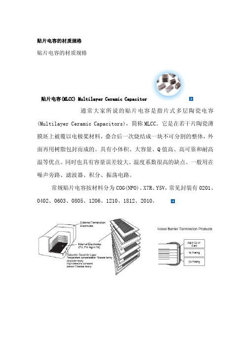
贴片电容的材质规格贴片电容的材质规格贴片电容(MLCC)Multilayer Ceramic Capacitor常规贴片电容按材料分为COG(NPO)、X7R、Y5V,常见封装有0201、0402、0603、0805、1206、1210、1812、2010。
NPO、X7R、Z5U和Y5V的主要区别是它们的填充介质不同。
在相同的体积下由于填充介质不同所组成的电容器的容量就不同,随之带来的电容器的介质损耗、容量稳定性等也就不同。
所以在使用电容器时应根据电容器在电路中作用不同来选用不同的电容器。
上表可看出各个不同材料的温度特性一 NPO电容器NPO是一种最常用的具有温度补偿特性的单片陶瓷电容器。
它的填充介质是由铷、钐和一些其它稀有氧化物组成的。
NPO电容器是电容量和介质损耗最稳定的电容器之一。
在温度从-55℃到+125℃时容量变化为0±30ppm/℃,电容量随频率的变化小于±0.3ΔC。
NPO电容的漂移或滞后小于±0.05%,相对大于±2%的薄膜电容来说是可以忽略不计的。
其典型的容量相对使用寿命的变化小于±0.1%。
NPO电容器随封装形式不同其电容量和介质损耗随频率变化的特性也不同,大封装尺寸的要比小封装尺寸的频率特性好。
NPO电容器适合用于振荡器、谐振器的槽路电容,以及高频电路中的耦合电容。
二 X7R电容器X7R电容器被称为温度稳定型的陶瓷电容器。
当温度在-55℃到+125℃时其容量变化为15%,需要注意的是此时电容器容量变化是非线性的。
X7R电容器的容量在不同的电压和频率条件下是不同的,它也随时间的变化而变化,大约每10年变化1%ΔC,表现为10年变化了约5%。
X7R电容器主要应用于要求不高的工业应用,而且当电压变化时其容量变化是可以接受的条件下。
它的主要特点是在相同的体积下电容量可以做的比较大。
三 Z5U电容器Z5U电容器称为”通用”陶瓷单片电容器。
国巨贴片电容知识
国巨贴片电容知识一、国巨贴片电容的命名:贴片电容的命名所包含的参数有贴片电容的尺寸、容值精度、贴片电容的材质、电压、电容容量、端头材料以及包装要求。
例如:国巨贴片电CC0805JRNPO9BN101容CC:表示国巨电容系列名称——多层陶瓷贴片电容。
国巨电容的系列还有CA(表示排容),CH(表示高频电容)等等。
0805:表示尺寸,长度为0.08英寸,宽度为0.05英寸。
此外,常见的电容尺寸还有0201,0402,0603,1206,1210,1808,1812等。
J:表示电容容量的误差精度为±5%;另外B=±0.1PF,C=±0.25PF,D=±0.5PF,F=±1PF,G=±2PF,K=±10%,M=±20%,Z=-20%~+80%。
R:表示7寸盘纸带包装。
NPO:表示电容材质。
此外,常用的电容材质还有X5R,X7R,Y5V。
9:表示电压为50V。
4=4V, 5=6.3V, 6=10V, 7=16V, 8=25V, 0=100V, A=200V, B=500V, C=1KV, D=2KV, E=3KV等(注意:100V是用数字0表示,不是字母O)B:表示端头材料是镍电极。
N:表示NPO。
101:表示容值,前面两个数字为有效数字,第三个数字表示有几个零。
101=100PF, 102=1000PF, 103=10,000PF……以此类推。
二、英制尺寸与公制尺寸的对应表:TDK贴片电容的参数识别积层贴片陶瓷片式电容器C 2012 X7R 1H 104 K T系列名称体积材料电压容量误差包装0603=0201 CH 0J=6.3V C=0.25 T=卷带1005=0402 COG 1A=10V D=0.5 B=袋装1608=0603 JB 1C=16V J=5%2012=0805 JF 1E=25V K=10%3216=1206 X7R 1H=50V M=20%3225=1210 X5R 2A=100V Z=+80-20%4532=1812 Y5V 2E=250V5650=2220 2J=630V4520=1808 3A=1KV3D=2KV3F=3KV。
TDK电容规格对照表
1. SCOPEThis specification is applicable to chip type multilayer ceramic capacitors with a priority over the other relevant specifications.Production places defined in this specification shall be TDK-EPC Corporation Japan,TDK (Suzhou) Co., Ltd and TDK Components U.S.A. Inc.EXPLANATORY NOTE:This specification warrants the quality of the ceramic chip capacitors. The chips should be evaluated or confirmed a state of mounted on your product.If the use of the chips goes beyond the bounds of the specification, we can not afford to guarantee.2. CODE CONSTRUCTION(Example)Catalog Number : C2012 X7R 1E 105 K A125 A (Web) (1) (2) (3) (4) (5) (6) (7) (8) Item Description : C2012 X7R 1E 105 K T xxxx(1) (2) (3) (4) (5) (9) (10)(1) TypePlease refer to product list for the dimension of each product.(2) Temperature Characteristics (Details are shown in table 1 No.7 and No.8 at page 5)(3) Rated Voltage(4) Rated CapacitanceStated in three digits and in units of pico farads (pF).The first and Second digits identify the first and second significant figures of the capacitance, the third digit identifies the multiplier.R is designated for a decimal point.Example 2R2 → 2.2pF105 → 1,000,000pF(5) Capacitance tolerance(6) Thickness code (Only Catalog Number)(7) Package code (Only Catalog Number)(8) Special code (Only Catalog Number)(9) Packaging (Only Item Description)(10) Internal code (Only Item Description)3. RATED CAPACITANCE AND CAPACITANCE TOLERANCE3.1 Standard combination of rated capacitance and tolerances5. STORING CONDITION AND TERM5 to 40°C at 20 to 70%RH6 months Max.6. P.C. BOARDWhen mounting on an aluminum substrate, large case sizes such as C3225, C4532 and C5750 types are more likely to be affected by heat stress from the substrate.Please inquire separate specification for the large case sizes when mounted on the substrate.7. INDUSTRIAL WASTE DISPOSALDispose this product as industrial waste in accordance with the Industrial Waste Law.8. PERFORMANCE(continued)(continued)(continued)(continued)*As for the initial measurement of capacitors (Class2) on number 8,12,13,14 and 15, leave capacitors at 150 -10,0°C for 1 hour and measure the value after leaving capacitors for 24 ± 2h in ambient condition.Dimensions (mm)TDK (EIA style) a b c C0402 (CC01005)0.2 0.8 0.2 C0603 (CC0201)0.3 0.8 0.3 C1005 (CC0402)0.4 1.5 0.5 C1608 (CC0603) 1.0 3.0 1.2 C2012 (CC0805) 1.2 4.0 1.65 C3216 (CC1206) 2.2 5.0 2.0 C3225 (CC1210) 2.2 5.0 2.9 C4532 (CC1812) 3.5 7.0 3.7 C5750 (CC2220)4.5 8.05.6Material : Glass Epoxy ( As per JIS C6484 GE4 )P .C. Board thickness : Appendix-2a 0.8mmAppendix-1a, 1b, 2b 1.6mmCopper ( thickness 0.035mm ) Solder resist9. INSIDE STRUCTURE AND MATERIALMATERIALNo. NAMEClass1 Class21 Dielectric CaZrO 3 BaTiO 32 ElectrodeNickel (Ni) 3 Copper (Cu) 4 Nickel(Ni) 5Termination Tin (Sn)10. RECOMMENDATIONAs for C3225, C4532 and C5750 types, It is recommended to provide a slit (about 1mm wide) in the board under the components to improve washing Flux. And please make sure to dry detergent up completely before.11. SOLDERING CONDITIONAs for C0402, C0603, C1005, C3225, C4532 and C5750 types, reflow soldering only.No. Process Condition2)Direct contact of the soldering iron with ceramic dielectric of chip capacitorsmay cause crack. Do not touch the ceramic dielectric and the terminations bysolder iron.5 Soldering5-7. Sn-Zn solderSn-Zn solder affects product reliability.Please contact TDK in advance when utilize Sn-Zn solder.5-8. Countermeasure for tombstoneThe misalignment between the mounted positions of the capacitors and the landpatterns should be minimized. The tombstone phenomenon may occur especiallythe capacitors are mounted (in longitudinal direction)in the same direction of thereflow soldering.(Refer to JEITA RCR-2335B Annex 1 (Informative) Recommendations to prevent thetombstone phenomenon)1) 2)If an unsuitable cleaning fluid is used, flux residue or some foreign articles may stick to chip capacitors surface to deteriorate especially the insulation resistance.If cleaning condition is not suitable, it may damage the chip capacitors.2)-1. Insufficient washing(1)(2)(3) Terminal electrodes may corrode by Halogen in the flux.Halogen in the flux may adhere on the surface of capacitors, and lower the insulation resistance.Water soluble flux has higher tendency to have above mentioned problems (1) and (2).2)-2. Excessive washingWhen ultrasonic cleaning is used, excessively high ultrasonic energy outputcan affect the connection between the ceramic chip capacitor's body and theterminal electrode. To avoid this, following is the recommended condition.Power : 20 W/ max.Frequency : 40 kHz max.Washing time : 5 minutes max.6Cleaning2)-3. If the cleaning fluid is contaminated, density of Halogen increases, and it maybring the same result as insufficient cleaning.10 Capacitance agingThe capacitors (Class 2) have aging in the capacitance. They may not be used in precision time constant circuit. In case of the time constant circuit, the evaluation should be done well. 11Estimated life and estimated failure rate of capacitorsAs per the estimated life and the estimated failure rate depend on the temperature and the voltage. This can be calculated by the equation described in JEITA RCR-2335B Annex 6 (Informative) Calculation of the estimated lifetime and the estimated failure rate ( Voltage acceleration coefficient : 3 multiplication rule, Temperature acceleration coefficient : 10°C rule)The failure rate can be decreased by reducing the temperature and the voltage but they will not be guaranteed.12 OthersCautionThe products listed on this specification sheet are intended for use in general electronic equipment (AV equipment, telecommunications equipment, homeappliances, amusement equipment, computer equipment, personal equipment, office equipment, measurement equipment, industrial robots) under a normal operation and use condition.The products are not designed or warranted to meet the requirements of theapplications listed below, whose performance and/or quality require a more stringent level of safety or reliability, or whose failure, malfunction or trouble could cause serious damage to society, person or property. Please understand that we are not responsible for any damage or liability caused by use of the products in any of the applications below or for any other use exceeding the range or conditions set forth in this specification sheet. If you intend to use the products in the applications listed below or if you have special requirements exceeding the range or conditions set forth in this specification, please contact us.(1) Aerospace/Aviation equipment(2) Transportation equipment (cars, electric trains, ships, etc.) (3) Medical equipment(4) Power-generation control equipment (5) Atomic energy-related equipment (6) Seabed equipment(7) Transportation control equipment(8) Public information-processing equipment (9) Military equipment(10) Electric heating apparatus, burning equipment (11) Disaster prevention/crime prevention equipment (12) Safety equipment(13) Other applications that are not considered general-purpose applicationsWhen designing your equipment even for general-purpose applications, you are kindly requested to take into consideration securing protection circuit/device or providing backup circuits in your equipment.13. Packaging labelPackaging shall be done to protect the components from the damage duringtransportation and storing, and a label which has the following information shall be attached.1) Inspection No.2) TDK P/N3) Customer's P/N4) Quantity*Composition of Inspection No.Example M2 A – ΟΟ– ΟΟΟ(a)(b) (c) (d) (e)a) Line codeb) Last digit of the yearc) Month and A for January and B for February and so on. (Skip I)d) Inspection Date of the month.e) Serial No. of the day14. Bulk packaging quantityTotal number of components in a plastic bag for bulk packaging: 1,000pcs.As for C0402, C0603 and C1005 types, not available for bulk packaging.15. TAPE PACKAGING SPECIFICATION1. CONSTRUCTION AND DIMENSION OF TAPING1-1. Dimensions of carrier tapeDimensions of paper tape shall be according to Appendix 3, 4. Dimensions of plastic tape shall be according to Appendix 5, 6. 1-2. Bulk part and leader of taping1-3. Dimensions of reelDimensions of Ø178 reel shall be according to Appendix 7, 8. Dimensions of Ø330 reel shall be according to Appendix 9, 10.1-4. Structure of tapingDrawing directionBottom cover tape(Bottom cover tape is not always applied.)2. CHIP QUANTITYChip quantity (pcs.) TypeThickness of chipTaping Material φ178mm reel φ330mm reelC0402 0.20 mm Paper 20,000 - C0603 0.30 mm Paper 15,000 - C1005 0.50 mm Paper 10,000 50,000 C1608 0.80 mmPaper 4,000 10,0000.60 mmPaper 0.85 mm Paper or Plastic4,000 C20121.25 mm Plastic 2,000 10,0000.60 mm Paper 0.85 mmPaper or Plastic4,0001.15 mm 1.30 mm 10,000 C32161.60 mm Plastic 2,0008,0001.15 mm 2,00010,0001.25 mm 1.30 mm1.60 mm 2,000 8,0002.00 mm 2.30 mm C32252.50 mm Plastic1,000 5,0001.60 mm2.00 mm1,0002.30 mm 2.50 mm 3,0002.80 mm C45323.20 mm Plastic5002,0002.00 mm2.30 mm 2.50 mm 3,000C57502.80 mmPlastic 5002,0003. PERFORMANCE SPECIFICATIONS3-1. Fixing peeling strength (top tape)0.05-0.7N. (See the following figure.)Direction of cover tape pullingDirection of pulling3-2. Carrier tape shall be flexible enough to be wound around a minimum radius of 30mm with components in tape.3-3. The missing of components shall be less than 0.1%3-4. Components shall not stick to fixing tape.3-5. The fixing tapes shall not protrude beyond the edges of the carrier tape not shall cover the sprocket holes.Appendix 3Paper TapePitch holeAppendix 4Paper Tape(Unit : mm)* The values in the parentheses ( ) are for reference.(Unit : mm)*The values in the parentheses ( ) are for reference.* As for 2.5mm thickness products, apply values in the brackets [ ].(Unit : mm)* The values in the parentheses ( ) are for reference.C0402, C0603, C1005, C1608, C2012, C3216, C3225( As for C3225 type, any thickness of the item except 2.5mm )(Material : Polystyrene)Symbol A B C D E W1 Dimension Ø178 ± 2.0 Ø60 ± 2.0Ø13 ± 0.5Ø21 ± 0.8 2.0 ± 0.5 9.0 ± 0.3 Symbol W2 rDimension 13.0 ± 1.4 1.0Appendix 8C3225, C4532, C5750 ( As for C3225 type, applied to 2.5mm thickness products )(Material : Polystyrene)Symbol W2 rDimension 17.0 ± 1.4 1.0C0603, C1005, C1608, C2012, C3216, C3225( As for C3225 type, any thickness of the item except 2.5mm )(Unit : mm) Symbol A B C D E WDimension Ø382 max.(NominalØ330)Ø50 min. Ø13 ± 0.5Ø21 ± 0.8 2.0 ± 0.5 10.0 ± 1.5Symbol t rDimension 2.0 ± 0.5 1.0Appendix 10C3225, C4532, C5750 ( As for C3225 type, applied to 2.5mm thickness products )Symbol A B C D E WDimension Ø382 max.(NominalØ330)Ø50 min. Ø13 ± 0.5Ø21 ± 0.8 2.0 ± 0.5 14.0 ± 1.5Symbol t r Dimension 2.0 ± 0.5 1.0。
TDK各大料号大全,TDK规格书大全,TDK最新版规格书
TDK电容C2012C0G1H472J0805NPO50V 4.7NF5%TDK电容C3216X5R1C106K1206X7R25V10UF10%TDK电容C3216X7R1H474K1206X7R50V0.47UF10%TDK电容C3216X7R1H684K1206X7R50V0.68UF10%TDK电容C3216X7R1H105K1206X7R50V1UF10%TDK电容C3216COG1H104J1206NPO50V0.1UF5%TDK新产品TDK电容C3216COG1H473J1206NPO50V0.047UF47NF5%TDK新产品TDK电容C3216X5R0J107M1206X5R 6.3V100UF20%TDK新产品TDk电容C3216X7T2J473K1206X7T630V47NF10%适用LED电源EMI 滤波,代替cbb插件电容TDK新品TDk电容C3216X7R2A104K1206X7R100V0.1UF(100NF)10%TDk电容C3216X7R2E104K1206X7R250V0.1UF(100NF)10%TDK电容C3216X5R1A476M1206X5R10V47UF20%TDK新产品TDK电容C3225X7R1H335K1210X7R50V 3.3UF10%TDK电容C3225X7R1E106K1210X7R25V10UF10%TDK电容C3225X7T1H106K1210X7T50V10UF10%封装TDK新产品TDK电容C3225X5R1C226K1210X7R25V22UF10%TDk电容C3225X7R2A225K1210X7R100V 2.2UF10%TDk电容C3225X7R1H475K1210X7R50V 4.7UF10%TDk电容C3225X5R1C336K1210X5R16V33UF20%TDk电容C3225X7T2W224K1210X7T450V0.22UF10%适用LED电源整流后滤波,代替cbb插件电容TDK新品TDk电容C3225X5R1C476M1210X5R16V47UF20%TDk电容C3225X5R1A476M1210X5R10V100UF20%TDK电容C4532COG2A104J1812NPO100V0.1UF5%新品TDK电容C4532COG2A473J1812NPO100V0.047UF47NF5%新品TDK电容C4532X7R2A105K1812X7R250V1UF10%TDK电容C4532X7R1H475K1812X7R50V 4.7UF10%TDK电容C4532X7R1E106K1812X7R25V10UF10%TDK电容C4532X5R1E226M1812X7R25V22UF10%TDk电容C4532X7R2E474K1812X7R100V0.47UF10%TDk电容C4532X5R0J107M1812X5R 6.3V100UF20%TDK电容C4532X7T2W334K1812X7T450V0.33UF适用220v阻容降压TDK电容C4532X7T2W474K1812X7T450V0.47UF适用220v阻容降压TDK电容C4532XT72W224K1812X7R450V0.22UF适用220v阻容降压TDk电容C5750X7R1H106K2220X7R50V10UF10%TDk电容C5750X7S2A106K2220X7S100V10UF10%TDK新品TDK电容C5750X7T2W105K2220X7S450V1UF适用于LED电源220V阻容降压,代替CBB插件电容TDK电容C5750Y5V1H226Z2220Y5V50V22UFTDK电容C5750Y5V1E476Z2220Y5V25V47UFTDK电容C5750Y5V1A107Z2220Y5V10V100UFTDK电容C5750Y5V1C107Z2220Y5V16V100UFTDK电容C5750X5R1A107M2220X5R10V100UFTDK电容C5750X5R0J107M2220X5R16V100UFTDK电容C5750X5R1A686M2220X5R10V68UFTDK电容C5750X5R1C336M2220X5R16V33UFTDK电容C5750X5R1E226M2220X5R25V22UFTDK电容C5750X5R1H106K2220X5R50V10UFTDK电容C5750X7R1C476M2220X7R16V47UFTDK电容C5750X7R1E226M2220X7R25V15UFTDK电容C5750X7R1E156M2220X7R25V 4.7UFTDK电容C5750X7R1H475K2220X7R50V 4.7UFTDK电容C5750X7R1H685K2220X7R50V 6.8UFTDK电容C5750X7R1H685M2220X7R50V 6.8UF20%TDK电容C5750X7R1H106M2220X7R50V10UF20%TDK电容C5750X7T2W684K2220X7T450V0.68UFTDK电容C5750X7R2E684K2220X7R250V0.68UFTDK电容C5750X7R2A105K2220X7R100V1UFTDK电容C5750X7T2J474K2220X7T630V0.47UFTDK电容C5750X7R2E474K2220X7R250V0.47UFTDK电容C5750X7R2A225M2220X7R100V 2.2UFTDK电容C5750X7R2A475K2220X7R100V 4.7UFTDK电容C5750X7R2A475M2220X7R100V 4.7U20%TDK电容C5750X7S2A685K2220X7S100V 6.8UF孙先生136********qq2877735032TDK共模电感(滤波器)ACM2012-900-2P-T002TDK原装新货TDK共模电感(滤波器)ACM7060-701-2PL-TL01TDK原装新货TDK贴片功率电感NLCV32T-2R2M-PF TDK原装新货TDK贴片功率电感NL453232T-102J-PF TDK原装新货TDK电感SLF6045T-1R5N4R0-3PFTDK电感SLF6045T-1R5N4R0-3PFTDK电感SLF6045T-2R2N3R3-3PFTDK电感SLF6045T-3R3N2R8-3PFTDK电感SLF6045T-4R7N2R4-3PFTDK电感SLF6045T-6R8N2R0-3PFTDK电感SLF6045T-100M1R6-3PFTDK电感SLF6045T-150M1R3-3PFTDK电感SLF6045T-220M1R1-3PFTDK电感VLCF4020T-100MR85TDK蜂鸣器PS1240P02CT3TDK-PS1240P02BT-蜂鸣器压电型70dB12.2MM制造商:TDK库存编号:制TDK蜂鸣器PS1240P02BT造商编号:PS1240P02BT输出音调类型:Low Frequency谐振频率:4kHz声压级SPL:70dB功能:Buzzer外径:12.2mm外部深度:6.5mm输出音调类型:Low Frequency谐振频率:4kHz声压级SPL:70dB功能:Buzzer外径:12.2mm外部深度:6.5mm详情咨询电话:1.利用贴片陶瓷电容器介质层的薄层化和多层叠层技术,使电容值大为扩大2.单片结构保证有极佳的机械性强度及可靠性3.极高的精确度,在进行自动装配时有高度的准确性4.因仅有陶瓷和金属构成,故即便在高温,低温环境下亦无渐衰的现象出现,具有较强可靠性与稳定性5.低集散电容的特性可完成接近理论值的电路设计6.残留诱导系数小,确保上佳的频率特性7.因电解电容器领域也获得了电容,故使用寿命延长,更造于具有高可靠性的电源8.由于esr低,频率特性良好,故最适合于高频,高密度类型的电源工作温度范围:-55~125℃额定电压:100vdc~3000vdc温度特性:npo:≤±30ppm/℃,-55~125℃(eia class i)x7r:≤±15%,-55~125℃(eia class ii)容量范围:npo:2pf to100nf;x7r:150pf to 2.2uf损失角正切(tanδ):npo:q≥1000;x7r:d.f.≤2.5%绝缘电阻:10gω或500/cω取两者最小值老化速率:npo:1%;x7r:2.5%一个decade时间日本tdk一级代理供应高频贴片电容,无线充电器专用,日本原装进口,大量现货,欢迎来电详询。
最全贴片电容规格书
贴片电容的材质规格贴片电容的材质规格贴片电容(MLCC)Multilayer Ceramic Capacitor常规贴片电容按材料分为COG(NPO)、X7R、Y5V,常见封装有0201、0402、0603、0805、1206、1210、1812、2010。
NPO、X7R、Z5U和Y5V的主要区别是它们的填充介质不同。
在相同的体积下由于填充介质不同所组成的电容器的容量就不同,随之带来的电容器的介质损耗、容量稳定性等也就不同。
所以在使用电容器时应根据电容器在电路中作用不同来选用不同的电容器。
上表可看出各个不同材料的温度特性一 NPO电容器NPO是一种最常用的具有温度补偿特性的单片陶瓷电容器。
它的填充介质是由铷、钐和一些其它稀有氧化物组成的。
NPO电容器是电容量和介质损耗最稳定的电容器之一。
在温度从-55℃到+125℃时容量变化为0±30ppm/℃,电容量随频率的变化小于±0.3ΔC。
NPO电容的漂移或滞后小于±0.05%,相对大于±2%的薄膜电容来说是可以忽略不计的。
其典型的容量相对使用寿命的变化小于±0.1%。
NPO电容器随封装形式不同其电容量和介质损耗随频率变化的特性也不同,大封装尺寸的要比小封装尺寸的频率特性好。
NPO电容器适合用于振荡器、谐振器的槽路电容,以及高频电路中的耦合电容。
二 X7R电容器X7R电容器被称为温度稳定型的陶瓷电容器。
当温度在-55℃到+125℃时其容量变化为15%,需要注意的是此时电容器容量变化是非线性的。
X7R电容器的容量在不同的电压和频率条件下是不同的,它也随时间的变化而变化,大约每10年变化1%ΔC,表现为10年变化了约5%。
X7R电容器主要应用于要求不高的工业应用,而且当电压变化时其容量变化是可以接受的条件下。
它的主要特点是在相同的体积下电容量可以做的比较大。
三 Z5U电容器Z5U电容器称为”通用”陶瓷单片电容器。
京瓷贴片电容名称规格
关于贴片电容的品名构成说明:(二)京瓷供贴片电容品名构成:京瓷供贴片电容名称构成共分9个部份:第一部份为:京瓷规定名称。
第二部份为:京瓷规格(尺寸)。
第三部份为:温度特性。
第四部份为:额定容量。
第五部份为:额定容量的允许偏差。
第六部份为:额定电压。
第七部份为:端电极处理形式。
第八部份为:包装方式。
第九部份为:选用品(特殊情况的选用)。
【例】:CM 21 X7R 105 K 10 A T 000①②③④⑤⑥⑦⑧⑨1.京瓷规定名称:记号用途CM普通应用CT薄形尺寸DM/DR汽车应用CF耐高压*CA多联型CU 高频用低ESR产品2.京瓷规格(尺寸):3.温度特性4.额定容量:容量大小一般由三位数字表示,前二位表示容量的有效值,第三位数字表示10的乘方(即0的个数),容量单位为PF。
代码容量R500.5PF1R0 1.0PF101100PF10310000PF5. 额定容量的允许偏差:代码A B C D F 偏差±01PF±0.1PF±0.25PF±.50PF±1PF 代码G J K M偏差±2%±5%±10%±206.额定电压:代码额定电压06京瓷OJ(村田,TDK)DC6.3V10京瓷1A(村田,TDK)DC10V16京瓷1C(村田,TDK)DC16V25京瓷1E(村田,TDK)DC25V50京瓷1H(村田,TDK)DC50V100京瓷2A(村田,TDK)DC100V200京瓷2D(村田,TDK)DC200V250京瓷2E(村田,TDK)DC250V400京瓷DC400V1000京瓷DC1000V2000京瓷DC2000V3000京瓷DC3000V4000京瓷DC4000V7.端电极处理形式:代码端电极A电镀8.包装方式:代码包装B散装(全品种)T编带(178mm直径/卷)H编带(178mm直径/卷)*L编带(330mm直径/卷)N编带(330mm直径/卷)*C盒装* H型、N型的文件插间隙为2mm.9.选用品(省略)。