5082-K111-0H000中文资料
5082-2800中文资料

Schottky Barrier Diodes for General Purpose ApplicationsTechnical DataFeatures• Low Turn-On VoltageAs Low as 0.34 V at 1 mA• Pico Second Switching Speed • High Breakdown VoltageUp to 70 V• Matched Characteristics AvailableDescription/Applications The 1N5711, 1N5712, 5082-2800/ 10/11 are passivated Schottky barrier diodes which use a patented “guard ring” design to achieve a high breakdown voltage. Packaged in a low cost glass package, they are well suited for high level detecting, mixing, switching, gating, log or A-D converting, video detecting, frequency discriminating, sampling, and wave shaping.The 5082-2835 is a passivatedSchottky diode in a low cost glasspackage. It is optimized for lowturn-on voltage. The 5082-2835 isparticularly well suited for theUHF mixing needs of the CATVmarketplace.The 5082-2300 Series and5082-2900 devices are unpas-sivated Schottky diodes in a glasspackage. These diodes haveextremely low 1/f noise and areideal for low noise mixing, andhigh sensitivity detecting. Theyare particularly well suited for usein Doppler or narrow band videoreceivers.1N57111N57125082-2300 Series5082-2800 Series5082-2900DIMENSIONS IN MILLIMETERS AND (INCHES).Outline 15Maximum RatingsJunction Operating and Storage Temperature Range5082-2303, -2900.................................................................-60°C to +100°C 1N5711, 1N5712, 5082-2800/10/11....................................-65°C to +200°C 5082-2835............................................................................-60°C to +150°C DC Power Dissipation(Measured in an infinite heat sink at T CASE = 25°C)Derate linearly to zero at maximum rated temperature5082-2303, -2900..............................................................................100 mW 1N5711, 1N5712, 5082-2800/10/11.................................................250 mW 5082-2835.........................................................................................150 mW Peak Inverse Voltage.................................................................................V BRPackage CharacteristicsOutline 15Lead Material........................................................................................DumetLead Finish..............................................................................95-5% Tin-LeadMax. Soldering Temperature................................................260°C for 5 secMin. Lead Strength....................................................................4 pounds pullTypical Package Inductance1N5711, 1N5712:................................................................................2.0 nH2800 Series:........................................................................................2.0 nH2300 Series, 2900:..............................................................................3.0 nHTypical Package Capacitance1N5711, 1N5712:................................................................................0.2 pF2800 Series:........................................................................................0.2 pF2300 Series, 2900:............................................................................0.07 pFThe leads on the Outline 15 package should be restricted so that thebend starts at least 1/16 inch from the glass body.Outline 15 diodes are available on tape and reel. The tape and reelspecification is patterned after RS-296-D.Electrical Specifications at T= 25°CAGeneral Purpose DiodesMin.Max.V F = 1 V Max.Max.Max.Breakdown Forward at Forward Reverse Leakage Capaci-Part Package Voltage Voltage Current Current tance Number Outline V BR (V)V F (mV)I F (mA)I R (nA) at V R (V)C T (pF) 5082-280015704101520050 2.0 1N571115704101520050 2.0 5082-281015204103510015 1.2 1N571215205503515016 1.2 5082-28111515410201008 1.2 5082-2835158*34010*1001 1.0 Test I R = 10 µA I F = 1 mA*V F = 0.45 V V R = 0 V Conditions*I R = 100 µA f =1.0 MHz Note: Effective Carrier Lifetime (τ) for all these diodes is 100 ps maximum measured with Krakauer method at 5 mA except for 5082-2835 which is measured at 20 mA.Low 1/f (Flicker) Noise DiodesMin.Max.V F = 1 V Max.Max.Max.Part Breakdown Forward at Forward Reverse Leakage Capaci-Number Package Voltage Voltage Current Current tance 5082-Outline V BR (V)V F (mV)I F (mA)I R (nA) at V R (V)C T (pF) 230315204003550015 1.0 29001510400201005 1.2 Test I R = 10 µA I F = 1 mA V R = 0 V Conditions f =1.0 MHzNote: Effective Carrier Lifetime (τ) for all these diodes is 100 ps maximum measured with Krakauer method at 20 mA.Matched Pairs and QuadsBasic Matched MatchedPart Number Pair Quad Batch5082-Unconnected Unconnected Matched[1]Test Conditions2900∆VF at IF= 1.0, 10 mA28005082-28045082-2805∆V F at I F = 0.5, 5 mA ∆V F = 20 mV∆V F = 20 mV*I F = 10 mA∆C O at f = 1.0 MHz28115082-2826∆VF at IF= 10 mA∆V F = 10 mV∆C O at f = 1.0 MHz ∆C O = 0.1 pF28355082-2080∆VF at IF=10 mA∆V F = 10 mV∆C O at f = 1.0 MHz∆C O = 0.1 pFNote:1. Batch matched devices have a minimum batch size of 50 devices.SPICE ParametersParameter Units5082-28005082-28105082-28115082-28355082-23035082-2900B V V75251892510C J0pF 1.60.8 1.00.70.7 1.1E G eV0.690.690.690.690.690.69I BV A10E-510E-510E-510E-510E-510E-5I S A 2.2 x 10E-9 1.1 x 10E-90.3 x 10E-8 2.2 x 10E-87 x 1.0E-910E-8N 1.08 1.08 1.08 1.08 1.08 1.08 R SΩ25101051015 P B V0.60.60.60.560.640.64 PT222222 M0.50.50.50.50.50.5Typical ParametersV F – FORWARD VOLTAGE (V)Figure 1. I-V Curve Showing Typical Temperature Variation for 5082-2300 Series and 5082-2900 Schottky Diodes.1001010.10.01I F - F O R W A R D C U R R E N T (m A )V BR (V)Figure 2. 5082-2300 Series Typical Reverse Current vs. Reverse Voltage at Various Temperatures.10.0001,000100101I R (n A )051015100755025T A = 25°CI F - FORWARD CURRENT (mA)Figure 3. 5082-2300 Series and 5082-2900 Typical Dynamic Resistance (R D ) vs. Forward Current (I F ).100010010R D - D Y N A M I C R E S I S T AN C E (Ω)0.01010100V R - REVERSE VOLTAGE (V)Figure 4. 5082-2300 and 5082-2900 Typical Capacitance vs. Reverse Voltage.1.21.00.80.60.40.20C T - C A P A C I T A N C E (p F )048121620V F - FORWARD VOLTAGE (V)Figure 5. I-V Curve Showing Typical Temperature Variation for 5082-2800 or 1N5711 Schottky Diodes.5010510.50.10.050.01I F - F O R W A R D C U R R E N T (m A )00.20.40.60.8 1.0 1.2V R - REVERSE VOLTAGE (V)Figure 6. (5082-2800 OR 1N5711) Typical Variation of Reverse Current (I R ) vs. Reverse Voltage (V R ) at Various Temperatures.100,00010,0001000100101I R - R E V E R S E C U R R E N T (n A )0.20.40.60.81.01.2V R - REVERSE VOLTAGE (V)Figure 7. (5082-2800 or 1N5711)Typical Capacitance (C T ) vs. Reverse Voltage (V R ).12.01.51.00.50C T - C A P A C I T A N C E (p F )010********V F - FORWARD VOLTAGE (V)Figure 8. I-V Curve Showing Typical Temperature Variation for the 5082-2810 or 1N5712 Schottky Diode.100101.00.10.01I F - F O R W A R D C U R R E N T (m A )V R - REVERSE VOLTAGE (V)Figure 9. (5082-2810 or IN5712)Typical Variation of Reverse Current (I R ) vs. Reverse Voltage (V R ) at Various Temperatures.10,0001000100101.0I R - R E V E R S E C U R R E N T (n A )Typical Parameters, continuedV F - FORWARD VOLTAGE (V)Figure 10. I-V Curve Showing Typical Temperature Variation for the 5082-2811 Schottky Diode.100101.00.10.01I F - F O R W A R D C U R R E N T (m A )0.40.20.60.81.01.2V R - REVERSE VOLTAGE (V)Figure 11. (5082-2811) Typical Variation of Reverse Current (I R ) vs. Reverse Voltage (V R ) at Various Temperatures.100,00010,0001000100101I R - R E V E R S E C U R R E N T (n A )0510********V F - FORWARD VOLTAGE (V)Figure 12. I-V Curve Showing Typical Temperature Variations for 5082-2835 Schottky Diode.100101.00.10.01I F - F O R W A R D C U R R E N T (m A )00.20.40.60.8 1.0 1.2V R - REVERSE VOLTAGE (V)Figure 13. (5082-2835) Typical Variation of Reverse Current (I R ) vs. Reverse Voltage (V R ) at Various Temperatures.100,00010,0001000100101I R - R E V E R S E C U R R E N T (n A )0123456V R - REVERSE VOLTAGE (V)Figure 14. Typical Capacitance (C T ) vs. Reverse Voltage (V R ).C T - C A P A C I T A N C E (p F )0246810I F - FORWARD CURRENT (mA)Figure 15. Typical Dynamic Resistance (R D ) vs. Forward Current (I F ).1000100101R D - D Y N A M I C R E S I S T A N C E (Ω)Diode Package Marking1N5xxx5082-xxxxwould be marked:1Nx xxxxx xxYWW YWWwhere xxxx are the last four digits of the 1Nxxxx or the 5082-xxxx partnumber. Y is the last digit of the calendar year. WW is the work week ofmanufacture.Examples of diodes manufactured during workweek45 of 1999:1N57125082-3080would be marked:1N53071280945945Data subject to change.Copyright © 1999 Agilent TechnologiesObsoletes 5968-4304E5968-7181E (11/99)。
HS00-00099中文资料

DRAFT
2007/08 EDITION MAGNETIC COMPONENTS SELECTOR GUIDE
We reserve the right to change specifications without prior notice
121
Pitch
50 mil 50 mil 50 mil 50 mil 50 mil 50 mil 50 mil 50 mil 50 mil 50 mil 50 mil 50 mil 50 mil 50 mil 50 mil 50 mil 100 mil 100 mil 100 mil 100 mil 100 mil 100 mil 100 mil 100 mil 100 mil 100 mil 100 mil 100 mil 100 mil 50 mil 50 mil 50 mil 50 mil 50 mil
Hi-Pot Length Width Height (Vrms)
12.70 12.70 12.70 12.70 12.70 12.70 12.70 12.70 12.70 12.70 12.70 12.70 12.70 12.70 12.70 12.70 25.40 25.40 25.40 25.40 23.37 25.40 25.40 20.20 25.40 20.20 20.20 20.20 25.40 29.80 29.80 29.80 29.80 29.80 9.65 9.65 9.65 9.40 9.65 9.65 9.65 9.35 9.53 9.40 9.65 9.53 9.53 9.53 9.53 9.65 12.70 12.70 12.70 12.70 13.20 12.70 12.70 10.18 10.50 10.18 10.18 10.18 5.33 16.26 16.26 16.26 16.26 16.26 6.22 6.22 6.22 5.08 6.22 6.22 6.22 6.22 6.22 5.08 6.22 5.08 5.08 6.22 6.22 6.22 7.00 7.00 7.00 7.00 6.35 7.00 7.00 6.50 6.35 6.50 6.50 6.50 11.43 6.95 6.95 6.95 6.95 6.95 1500 1500 2000 1500 2000 1500 1500 1500 1500 2000 2000 1500 1500 1500 1500 2000 1500 1500 1500 1500 1500 1500 1500 2000 1500 1500 1500 1500 1500 1500 1500 1500 1500 1500
危险化学品特性表
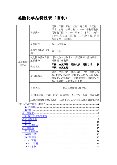
危险化学品特性表(自制)(1)丙烯酸 (3)(2)甲酸 (4)(3)氢氟酸 (5)(1)N,N-二甲基甲酰胺 (7)(2)丙烯酸丁酯 (8)(1)萘 (10)(2)乌洛托品 (11)(1)氯酸钠 (13)(2)亚硝酸钠 (14)(1)四氯乙烯 (15)(2)二氯甲烷 (17)3.1。
1.1丙酮 (18)3。
1.1。
2-丁酮 (19)3。
1.1.3甲醇 (21)3.1。
1。
4乙醇 (22)3.1。
1.5 环己酮 (24)3.1。
1。
6异丙醇 (25)3.1.1.7 甲苯 (27)3。
1。
1。
8 1,2—二甲苯 (28)3。
1.1。
9 乙醚 (30)3.1。
1.10 乙酸乙酯 (32)3.1.1。
11过氧化氢 (33)3。
1。
1.12高锰酸钾 (35)3.1.1。
13重铬酸钾 (36)3。
1。
1。
14硝酸银 (37)3.1。
1.15苯酚 (39)3.1.1。
16三氯甲烷 (41)3.1。
1。
17四氯化碳 (42)3。
1.1。
18氢氧化铵水溶液 (44)3。
1。
1。
19氢氧化钠 (45)3。
1。
1。
20氢氧化钾 (46)3。
1.1。
21甲醛 (47)3。
1。
1。
22盐酸 (49)3.1。
1.23硝酸 (51)3。
1。
1。
24硫酸 (52)3.1。
1。
25 乙酸 (54)3。
1.1。
26三氯乙酸 (56)3.1。
1。
27氢氟酸 (57)3.1.1。
28次氯酸钠 (59)3.1。
1.29亚硫酸氢钠 (60)(4)纯苯 (62)(5)1,1—二氯乙烷 (63)(7)正丁醇 (65)(10)二(正)丁醚 (66)(11)丙烯酸正丁酯 (68)(4)冰醋酸 (69)三氯乙醛 (70)硝酸钠 (72)连二亚硫酸钠 (73)石油醚 (74)对二甲苯 (76)氧 (77)乙炔 (78)⑺乙酸酐 (79)⑻2—丁酮 (81)(1)丙烯酸表3。
1—1 丙烯酸简介(2)甲酸表3.1-2甲酸简介(3)氢氟酸表3.1—3氢氟酸简介(1)N,N-二甲基甲酰胺表3。
Lubchem润滑脂
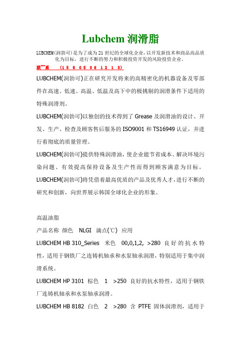
Lubchem润滑脂LUBCHEM(润勃可)是为了成为21世纪的全球化企业,以开发新技术和商品高品质化为目标,进行不断的努力和积极投资开发的风险投资企业。
联~~系(1 5 8 0 5 0 6 1 2 1 3)LUBCHEM(润勃可)正在研究开发将来的高精密化的机器设备及零部件在高速、低速、高温、低温及高下中的极挑剔的润滑条件下适用的特殊润滑剂。
LUBCHEM(润勃可)以独创的技术得到了Grease及润滑油的设计、开发、生产、检查及顾客售后服务的ISO9001和TS16949认证,并进行着彻底的质量管理。
LUBCHEM(润勃可)提供特殊润滑油,使企业能节省成本、解决环境污染问题、有效提高保持设备及生产性而得到顾客满意为目标。
LUBCHEM(润勃可)将凭借着最高优质的产品及优秀人才,进行不断的研究和创新,向世界展示韩国全球化企业的形象。
高温油脂产品名称颜色NLGI 滴点(℃) 应用LUBCHEM HB 310_Series 米色00,0,1,2, >280 良好的抗水特性,适用于钢铁厂之连铸机轴承和水泵轴承润滑,特别适用于集中润滑系统。
LUBCHEM HP 3101 棕色 1 >250 良好的抗水特性,适用于钢铁厂连铸机轴承和水泵轴承润滑。
LUBCHEM HB 8182 白色 2 >280 含PTFE固体润滑剂,适用于铁水输送小车轴承的润滑。
LUBCHEM BH 6052 CR 红色 2 >250 良好的极压特性,用于球轴承的润滑,适用于高温及高压多用途。
LUBCHEM SS 6042 棕色 2 >280 高温多用途润滑脂,适用于汽车车轮轴承,风扇马达轴承及纺织机械轴承润滑。
LUBCHEM HB 3602 米色 2 >280 适合电机轴承长效润滑。
LUBCHEM HM 7052 M 黑色 2 >260 含固体润滑剂,适用于需延长加脂周期或难以加脂的场合。
LUBCHEM BH 3092 F 白色00,0,1,2, None 杰出的高温特性,基于合成基础油制造,适用于钢厂辊轧设备,造纸设备轴承。
TK000-经典通用宝藏文档
伸缩器制造安装记录
鲁TK-034
结论
总监理工程师签字: 年 月 日
山东省建设工程质量监督总站监制
7
建筑安装工程装备、成品、半成品、材料合格证汇总表
鲁TK-006
8
装备(开箱)进场验收记录
鲁TK-007
9
材料、成品、半成品进场验收记录
鲁TK-008
10
合格证贴条
鲁TK-009
11
复印件(或抄件)贴条
鲁TK-010
12
阀门(清洗)实验记录
鲁TK-011
13
管道隐蔽工程验收记录
鲁TK-012
14
水、气压实验记录
鲁TK-028
30
风口平衡实验(调解)记录
鲁TK-029
31
防腐施工记录
鲁TK-030
32
绝热施工记录
鲁TK-031
33
透风空调装备单机试运转及调试记录
鲁TK-032
34
透风空调零碎无消费负荷下的联合试运转及调试记录
鲁TK-033-1
35
透风空调零碎无消费负荷下的联合试运转及调试记录附表
鲁TK-033-2
鲁TK-021
23
制冷零碎气密性实验记录
鲁TK-022
24
净化空调零碎风管清洗记录
鲁TK-023
25
现场组装除尘器、空调机漏风检测记录
鲁TK-024
26
工序交接记录
鲁TK-025
27
透风空调装备、管道(防静电)接地检查验收记录
鲁TK-026
28
透风安装普通性检查记录
鲁TK-027
29
空调安装普通性检查记录
66605X-XXX-EN
WARNING STATIC SPARK. Can cause explosion resulting in severe injury or death. Ground pump and pumping system.
(800) 495-0276 FAX(800) 892-6276
© 2010 CCN 99449712
OPERATING AND SAFETY PRECAUTIONS
READ, UNDERSTAND AND FOLLOW THIS INFORMATION TO AVOID INJURY AND PROPERTY DAMAGE.
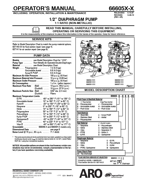
E.P.R. . . . . . . . . . . . . . . . . -60_ to 280_ F (-51_ to 138_ C) Groundable Acetal . . . . . . . 10_ to 180_ F (-12_ to 82_ C) HytrelR . . . . . . . . . . . . . . -20_ to 150_ F (-29_ to 66_ C) Neoprene . . . . . . . . . . . . . 0_ to 200_ F (-18_ to 93_ C) Nitrile . . . . . . . . . . . . . . . . 10_ to 180_ F (-12_ to 82_ C) Polypropylene . . . . . . . . . . 35_ to 175_ F (2_ to 79_ C) Polyurethane . . . . . . . . . . . 10_ to 150_ F (-12_ to 66_ C) Kynar PVDF . . . . . . . . . . . 10_ to 200_ F (-12_ to 93_ C) SantopreneR . . . . . . . . . . -40_ to 225_ F (-40_ to 107_ C) PTFE . . . . . . . . . . . . . . . . 40_ to 225_ F (4_ to 107_ C) VitonR . . . . . . . . . . . . . . . -40_ to 350_ F (-40_ to 177_ C) Groundable . . . . . . . . . . . 666056-X and 66605H-X models only Dimensional Data . . . . . . . . . . . . . . . . see page 8 Noise Level @ 70 p.s.i., 60 c.p.m. . . . . . 71.1 db(A)
H600 系列类K5与H罐孔熔断器数据清单说明书

Catalog Symbol:H600 Series Amp Rating: 1⁄10to 600A Voltage Rating:600V Agency Information:CE, UL Listed, UL 4248, Guide IZLT, File E14853CSA Certified, C22.2 No. 39, Class 6225-01, File 47235Withstand Rating (SCCR):10,000A RMS Sym.For use with Class K5 & H Fuses (Cooper Bussmann NOS and RES)UL Flammability:94V0Materials:Thermoplastic600V Class H Fuse BlocksH600 SeriesClass H Fuseblocks (600V) Catalog Data (for NOS and RES Fuses)Terminal Type (Suffix No.)ScrewBox Lug w/⁄01H60030-1S SR P PR C CR 1C, CR #2-14 Cu, #2-12 Al to 2H60030-2S SR P PR C CR 2P , PR, S, SR #10-18 Cu ONLY303H60030-3S SR P PR C CR 3311H60060-1————C CR 4 to 2H60060-2— —— — C CR 5C, CR #2-14 Cu, #2-8 Al603H60060-3— —— — C CR 6611H60100-1— — — —— CR 7to 2H60100-2— — — —— CR 8CR #1/0-8 Cu/Al1003H60100-3— — — —— CR 91011H60200-1— —— ——CR10CR 250kcmil-6 Cu/Alto2003H60200-3— —— —— CR 112011H60400-1— —— —— CR ‡12CR 500kcmil-4 Cu/Alto4003H60400-3— —— ——CR†134011H60600-1— —— —— CR 14CR (2) 500kcmil-4/0 Cu/Alto6003H60600-3— —— ——CR†15†No UL, No CSA Certification.‡UL Recognized, CSA CertificationPressure PlatePressure Plate & Clip with Reinforced SpringWire RangeClip with Reinforced Spring—Figure NumberAmpsCatalog NumberClip with Reinforced Spring—PolesDimensions – in600V, 1⁄10to 30AFIGURE 7.FIGURE 8.FIGURE 9.600V , 101 to 200A600V , 201 to 400A600V , 401 to 600AFIGURE 12.FIGURE 14.The only controlled copy of this Data Sheet is the electronic read-only version located on the Cooper Bussmann Network Drive. All other copies of this document are by definition uncontrolled. This bulletin is intended to clearly present comprehensive product data and provide technical information that will help the end user with design applications. Cooper Bussmann reserves the right, without notice, to change design or construction of any products and to discontinue or limit distribution of any products. Cooper Bussmann also reserves the right to change or update, without notice, any technical infor-mation contained in this bulletin. Once a product has been selected, it should be tested by the user in all possible applications.。
5082-E107-EG000中文资料
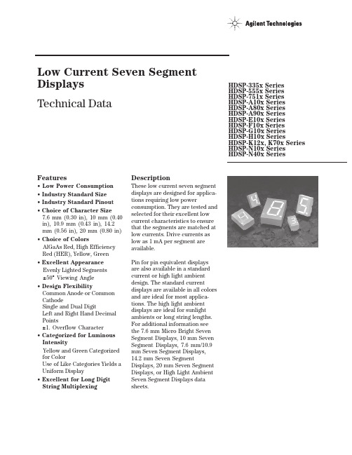
Features• Low Power Consumption • Industry Standard Size• Industry Standard Pinout • Choice of Character Size7.6 mm (0.30 in), 10 mm (0.40 in), 10.9 mm (0.43 in), 14.2 mm (0.56 in), 20 mm (0.80 in)• Choice of ColorsAlGaAs Red, High Efficiency Red (HER), Yellow, Green• Excellent Appearance Evenly Lighted Segments±50° Viewing Angle• Design FlexibilityCommon Anode or Common CathodeSingle and Dual DigitLeft and Right Hand Decimal Points±1. Overflow Character• Categorized for Luminous IntensityYellow and Green Categorized for ColorUse of Like Categories Yields a Uniform Display• Excellent for Long Digit String Multiplexing DescriptionThese low current seven segment displays are designed for applica-tions requiring low power consumption. They are tested and selected for their excellent low current characteristics to ensure that the segments are matched at low currents. Drive currents as low as 1 mA per segment are available.Pin for pin equivalent displays are also available in a standard current or high light ambient design. The standard current displays are available in all colors and are ideal for most applica-tions. The high light ambient displays are ideal for sunlight ambients or long string lengths. For additional information see the 7.6 mm Micro Bright Seven Segment Displays, 10 mm Seven Segment Displays, 7.6 mm/10.9 mm Seven Segment Displays, 14.2 mm Seven Segment Displays, 20 mm Seven Segment Displays, or High Light Ambient Seven Segment Displays data sheets.Low Current Seven SegmentDisplays Technical Data HDSP-335x SeriesHDSP-555x SeriesHDSP-751x SeriesHDSP-A10x Series HDSP-A80x Series HDSP-A90x Series HDSP-E10x Series HDSP-F10x Series HDSP-G10x Series HDSP-H10x Series HDSP-K12x, K70x Series HDSP-N10x SeriesHDSP-N40x SeriesDevicesAlGaAs HER Yellow Green Package HDSP-HDSP-HDSP-HDSP-Description Drawing A1017511A801A9017.6 mm Common Anode Right Hand Decimal A A1037513A803A9037.6 mm Common Cathode Right Hand Decimal B A1077517A807A9077.6 mm Common Anode ±1. Overflow C A1087518A808A9087.6 mm Common Cathode ±1. Overflow D F10110 mm Common Anode Right Hand Decimal E F10310 mm Common Cathode Right Hand Decimal F F10710 mm Common Anode ±1. Overflow G F10810 mm Common Cathode ±1. Overflow H G10110 mm Two Digit Common Anode Right Hand Decimal X G10310 mm Two Digit Common Cathode Right Hand Decimal Y E100335010.9 mm Common Anode Left Hand Decimal I E101335110.9 mm Common Anode Right Hand Decimal J E103335310.9 mm Common Cathode Right Hand Decimal K E106335610.9 mm Universal ±1. Overflow[1]L H101555114.2 mm Common Anode Right Hand Decimal M H103555314.2 mm Common Cathode Right Hand Decimal N H107555714.2 mm Common Anode ±1. Overflow O H108555814.2 mm Common Cathode ±1. Overflow P K121K70114.2 mm Two Digit Common Anode Right Hand Decimal R K123K70314.2 mm Two Digit Common Cathode Right Hand Decimal S N10020 mm Common Anode Left Hand Decimal Q N101N40120 mm Common Anode Right Hand Decimal T N103N40320 mm Common Cathode Right Hand Decimal U N10520 mm Common Cathode Left Hand Decimal V N106N40620 mm Universal ±1. Overflow[1]W Note:1. Universal pinout brings the anode and cathode of each segment’s LED out to separate pins. See internal diagrams L or W.Part Numbering System5082-x xx x-x x x xxHDSP-x xx x-x x x xxMechanical Options[1]00: No mechanical optionColor Bin Options[1,2]0: No color bin limitationMaximum Intensity Bin[1,2]0: No maximum intensity bin limitationMinimum Intensity Bin[1,2]0: No minimum intensity bin limitationDevice Configuration/Color[1]G: GreenDevice Specific Configuration[1]Refer to respective datasheetPackage[1]Refer to Respective datasheetNotes:1. For codes not listed in the figure above, please refer to the respective datasheet or contact your nearest Agilent representative fordetails.2. Bin options refer to shippable bins for a part-number. Color and Intensity Bins are typically restricted to 1 bin per tube (excep-tions may apply). Please refer to respective datasheet for specific bin limit information.Package DimensionsPackage Dimensions (cont.)Package Dimensions (cont.)*The Side View of package indicates Country of Origin.Package Dimensions (cont.)Package Dimensions (cont.)Package Dimensions (cont.)Internal Circuit DiagramInternal Circuit Diagram (cont.)Absolute Maximum RatingsAlGaAs Red - HDSP-HERA10X/E10X/H10X HDSP-751X/Yellow GreenK12X/N10X/N40X335X/555X/HDSP-A80X HDSP-A90X Description F10X, G10X Series K70X Series Series Series Units Average Power per Segment or DP375264mW Peak Forward Current per 45mA Segment or DPDC Forward Current per15[1]15[2]mA Segment or DPOperating Temperature Range-20 to +100-40 to +100°C Storage Temperature Range -55 to +100°C Reverse Voltage per Segment 3.0V or DPWave Soldering Temperature for 3Seconds (1.60 mm [0.063 in.] below 250°C seating body)Notes:1. Derate above 91°C at 0.53 mA/°C.2. Derate HER/Yellow above 80°C at 0.38 mA/°C and Green above 71°C at 0.31 mA/°C.Electrical/Optical Characteristics at T A = 25°CAlGaAs RedDeviceSeriesHDSP-Parameter Symbol Min.Typ.Max.Units Test Conditions315600I F = 1 mA A10x3600I F = 5 mA330650I F = 1 mAF10x, G10x3900I F = 5 mA390650I F = 1 mA E10x Luminous Intensity/Segment[1,2]I Vµcd(Digit Average)3900I F = 5 mA400700I F = 1 mAH10x, K12x4200I F = 5 mA270590I F = 1 mAN10x, N40x3500I F = 5 mA1.6I F = 1 mAForward Voltage/Segment or DP V F 1.7V I F = 5 mA1.82.2I F = 20 mA PkAll Devices Peak WavelengthλPEAK645nmDominant Wavelength[3]λd637nmReverse Voltage/Segment or DP[4]V R 3.015V I R = 100 µATemperature Coefficient of∆V F/°C-2 mV mV/°CV F/Segment or DPA10x255F10x, G10x320E10x340Thermal Resistance LED RθJ-PIN°C/W/SegH10x, K12x Junction-to-Pin400N10x, N40x430High Efficiency RedDeviceSeriesHDSP-Parameter Symbol Min.Typ.Max.Units Test Conditions160270I F = 2 mA 751x1050I F = 5 mA200300I F = 2 mA Luminous Intensity/Segment[1,2]I V mcd(Digit Average)1200I F = 5 mA335x, 555x,K70x270370I F = 2 mA1480I F = 5 mA1.6I F = 2 mAForward Voltage/Segment or DP V F 1.7V I F = 5 mA2.1 2.5I F = 20 mA Pk All Devices Peak WavelengthλPEAK635nmDominant Wavelength[3]λd626nmReverse Voltage/Segment or DP[4]V R 3.030V I R = 100 µATemperature Coefficient of∆V F/°C-2mV/°CV F/Segment or DP751x200335x Thermal Resistance LED RθJ-PIN280°C/WJunction-to-Pin555x, K70x345YellowDeviceSeriesHDSP-Parameter Symbol Min.Typ.Max.Units Test Conditions Luminous Intensity/Segment[1,2]250420I F = 4 mA(Digit Average)I V mcd1300I F = 10 mA1.7I F = 4 mAForward Voltage/Segment or DP V F 1.8V I F = 5 mA A80x2.1 2.5I F = 20 mA PkPeak WavelengthλPEAK583nmDominant Wavelength[3,5]λd581.5585592.5nmReverse Voltage/Segment or DP[4]V R 3.030V I R = 100 µATemperature Coefficient of∆V F/°C-2mV/°CV F/Segment or DPThermal Resistance LED RθJ-PIN200°C/WJunction-to-PinGreenDeviceSeriesHDSP-Parameter Symbol Min.Typ.Max.Units Test Conditions Luminous Intensity/Segment[1,2]250475I F = 4 mA(Digit Average)I V mcd1500I F = 10 mA1.9I F = 4 mAForward Voltage/Segment or DP V F 2.0V I F = 10 mA A90x2.1 2.5I F = 20 mA PkPeak WavelengthλPEAK566nmDominant Wavelength[3,5]λd571577nmReverse Voltage/Segment or DP[4]V R 3.030V I R = 100 µATemperature Coefficient of∆V F/°C-2mV/°CV F/Segment or DPThermal Resistance LED RθJ-PIN200°C/WJunction-to-PinNotes:1. Device case temperature is 25°C prior to the intensity measurement.2. The digits are categorized for luminous intensity. The intensity category is designated by a letter on the side of the package.3. The dominant wavelength, λd, is derived from the CIE chromaticity diagram and is the single wavelength which defines the color of thedevice.4. Typical specification for reference only. Do not exceed absolute maximum ratings.5. The yellow (HDSP-A800) and Green (HDSP-A900) displays are categorized for dominant wavelength. The category is designated by anumber adjacent to the luminous intensity category letter.AlGaAs RedIntensity Bin Limits (mcd)AlGaAs RedHDSP-A10xIV Bin Category Min.Max.E0.3150.520F0.4280.759G0.621 1.16H0.945 1.71I 1.40 2.56J 2.10 3.84K 3.14 5.75L 4.708.55HDSP-E10x/F10x/G10xIV Bin Category Min.Max.D0.3910.650E0.5320.923F0.755 1.39G 1.13 2.08H 1.70 3.14HDSP-H10x/K12xIV Bin Category Min.Max.C0.4150.690D0.5650.990E0.810 1.50F 1.20 2.20G 1.80 3.30H 2.73 5.00I 4.097.50HDSP-N10xIV Bin Category Min.Max.A0.2700.400B0.3250.500C0.4150.690D0.5650.990E0.810 1.50F 1.20 2.20G 1.80 3.30H 2.73 5.00I 4.097.50Intensity Bin Limits (mcd), continued HERHDSP-751xIV Bin Category Min.Max.B0.1600.240C0.2000.300D0.2500.385E0.3150.520F0.4280.759G0.621 1.16HDSP-751xIV Bin Category Min.Max.B0.2400.366C0.3000.477D0.3910.650E0.5320.923F0.755 1.39G 1.13 2.08H 1.70 3.14HDSP-555x/K70xIV Bin Category Min.Max.A0.2700.400B0.3250.500C0.4150.690D0.5650.990E0.810 1.50F 1.20 2.20G 1.80 3.30H 2.73 5.00I 4.097.50Intensity Bin Limits (mcd), continued YellowHDSP-A80xIV Bin Category Min.Max.D0.2500.385E0.3150.520F0.4250.760G0.625 1.14H0.940 1.70I 1.40 2.56J 2.10 3.84K 3.14 5.76L 4.718.64M7.0713.00N10.6019.40O15.9029.20P23.9043.80Q35.8065.60GreenHDSP-A90xIV Bin Category Min.Max.E0.3150.520F0.4250.760G0.625 1.14H0.940 1.70I 1.40 2.56J 2.10 3.84K 3.14 5.76L 4.718.64M7.0713.00N10.6019.40O15.9029.20P23.9043.80Q35.8065.60Electrical/OpticalFor more information on electrical/optical characteristics, please see Application Note 1005.Contrast Enhancement For information on contrast enhancement, please see Application Note 1015.Soldering/Cleaning Cleaning agents from the ketone family (acetone, methyl ethyl ketone, etc.) and from the chorinated hydrocarbon family (methylene chloride, trichloro-ethylene, carbon tetrachloride, etc.) are not recommended for cleaning LED parts. All of these various solvents attack or dissolve the encapsulating epoxies used to form the package of plastic LED parts.For information on soldering LEDs, please refer to Application Note 1027.Note:All categories are established for classification of products. Productsmay not be available in all categories. Please contact your localAgilent representatives for further clarification/information.Color Categories/semiconductorsFor product information and a complete list ofdistributors, please go to our web site.For technical assistance call:Americas/Canada: +1 (800) 235-0312 or(916) 788 6763Europe: +49 (0) 6441 92460China: 10800 650 0017Hong Kong: (+65) 6271 2451India, Australia, New Zealand: (+65) 6271 2394Japan: (+81 3) 3335-8152(Domestic/International), or0120-61-1280(Domestic Only)Korea: (+65) 6271 2194Malaysia, Singapore: (+65) 6271 2054Taiwan: (+65) 6271 2654Data subject to change.Copyright © 2005 Agilent Technologies, Inc.Obsoletes 5988-8412ENJanuary 19, 20055989-0080EN。
- 1、下载文档前请自行甄别文档内容的完整性,平台不提供额外的编辑、内容补充、找答案等附加服务。
- 2、"仅部分预览"的文档,不可在线预览部分如存在完整性等问题,可反馈申请退款(可完整预览的文档不适用该条件!)。
- 3、如文档侵犯您的权益,请联系客服反馈,我们会尽快为您处理(人工客服工作时间:9:00-18:30)。
DevicesAlGaAs Orange Red HER Green Package HDSP-HDSP-HDSP-HDSP- DescriptionDrawingA411A111A211A5117.6 mm Common Anode Right Hand Decimal A A413A113A213A5137.6 mm Common Cathode Right Hand Decimal B F411F111F211F51110 mm Common Anode Right Hand Decimal C F413F113F213F51310 mm Common Cathode Right Hand Decimal D G411G111G211G51110 mm Two Digit Common Anode Right Hand Decimal E G413G113G213G51310 mm Two Digit Common Cathode Right Hand Decimal F H411H111H211H51114.2 mm Common Anode Right Hand Decimal G H413H113H213H51314.2 mm Common Cathode Right Hand Decimal H K411K111K211K51114.2 mm Two Digit Common Anode Right Hand Decimal I K413K113K213K51314.2 mm Two Digit Common Cathode Right Hand DecimalJBlack Surface Seven Segment Displays Technical DataFeatures• Black Surface and Color Tinted Epoxy• Industry Standard Size • Industry Standard Pinout • Choice of Character Size 7.6 mm (0.30 in.), 10 mm (0.40in.), 14.2 mm (0.56 in.)• Choice of ColorsAlGaAs Red, High Efficiency Red (HER), Green, Orange • Excellent Appearance Evenly Lighted Segments ±50° Viewing Angle• Design FlexibilityCommon Anode or Common CathodeSingle and Two Digit• Categorized for Luminous IntensityCategorized for Color: Green Use of Like Categories Yields a Uniform Display• Excellent for Long Digit String MultiplexingDescriptionThese devices use industrystandard size package and pinout.Available with black surfaceHDSP-AX11/-AX13 Series HDSP-FX11/-FX13 Series HDSP-GX11/-GX13 Series HDSP-HX11/-HX13 Series HDSP-KX11/-KX13 Seriesfinish. All devices are available as either common anode or common cathode.Typical applications includeappliances, channel indicators of TV, CATV converters, game machines, and point of sale terminals.Part Numbering System5082 -X X X X-X X X X XHDSP-X X X X-X X X X XMechanical Options[1]00: No Mechanical OptionColor Bin Options[1,2]0: No Color Bin LimitationMaximum Intensity Bin[1,2]0: No Maximum Intensity Bin LimitationMinimum Intensity Bin[1,2]0: No Minimum Intensity Bin LimitationDevice Configuration/Color[1]1: Common Anode3: Common CathodeDevice Specific Configuration[1]Refer to Respective DatasheetPackage[1]A: 7.6 mm (0.3 inch) Single Digit Seven Segment DisplayF: 10 mm (0.4 inch) Single Digit Seven Segment DisplayG: 10 mm (0.4 inch) Dual Digit Seven Segment DisplayH: 14.2 mm (0.56 inch) Single Digit Seven Segment DisplayK: 14.2 mm (0.56 inch) Dual Digit Seven Segment Display Notes:1. For codes not listed in the figure above, please refer to the respective datasheet or contact your nearestAgilent representative for details.2. Bin options refer to shippable bins for a part number. Color and Intensity Bins are typically restricted to 1bin per tube (exceptions may apply). Please refer to respective datasheet for specific bin limit information.Package Dimensions (7.6 mm Series)Internal Circuit DiagramPackage Dimensions (10 mm Series: Single)Internal Circuit DiagramPackage Dimensions (10 mm Series: Two Digit)Internal Circuit DiagramPackage Dimensions (14.2 mm Series: Single)Internal Circuit DiagramPackage Dimensions (14.2 mm Series: Two Digit)Internal Circuit Diagram2DIGIT NO. 1 CATHODE1Absolute Maximum RatingsAlGaAs Red HER/Orange GreenHDSP-X11X HDSP-X21X/X41X HDSP-X51X Description Series Series Series Units Average Power per Segment37105105mW or DPPeak Forward Current per4590[1]90[3]mA Segment or DPDC Forward Current per15[5]30[2]30[4]mA Segment or DPOperating Temperature Range–20 to +100 –40 to +100°C Storage Temperature Range–55 to +100°C Reverse Voltage per 3.0V Segment or DPWave Soldering Temperature for250°C 3 Seconds (1.60 mm [0.063 in.]below Body)Notes:1. See Figure 5 to establish pulsed conditions.2. Derate above 53°C at 0.45 mA/°C (see Figure 7).3. See Figure 6 to establish pulsed conditions.4. Derate above 39°C at 0.37 mA/°C (see Figure 7).5. Derate above 91°C at 0.53 mA/°C (see Figure 1).Electrical/Optical Characteristics at T A = 25°CAlGaAs RedDevice SeriesHDSP-Parameter Symbol Min.Typ.Max.Units Test Conditions A11X Luminous Intensity/Segment[1,2]I V315600µcd I F = 1 mA (Digit Average)3600I F = 5 mAF11X, G11X330650I F = 1 mA3900I F = 5 mAH11X, K11X400700I F = 1 mA4200I F = 5 mAAll Devices Forward Voltage/Segment or DP V F 1.6 2.0V I F = 1 mA1.7I F = 5 mA1.822I F = 20 mA PeakPeak WavelengthλP EAK645nmDominant Wavelength[3]λd637nmReverse Voltage/Segment or DP[4]V R 3.015V I R = 100 µATemperature Coefficient of∆V F/°C-2mV/°CV F/Segment or DPA11X Thermal Resistance LED RθJ-PIN255°C/W/Junction-to-Pin Seg.F11X, G11X320H11X, K12X400OrangeDevice SeriesHDSP-Parameter Symbol Min.Typ.Max.Units Test Conditions A41X Luminous Intensity/Segment I V0.70mcd I F = 5 mA (Segment Average)[1,2]F41X, G41X 1.0I F = 5 mAH41X, K41X 2.37I F = 10 mAAll Forward Voltage/Segment or DP V F 2.0 2.5V I F = 20 mA DevicesPeak WavelengthλPEAK600nmDominant Wavelength[3]λd603nmReverse Voltage/Segment or DP[4]V R 3.030V I R = 100 µATemperature Coefficient of∆V F/°C–2mV/°CV F/Segment or DPA41X Thermal Resistance LED RθJ-PIN200°C/W/Junction-to-Pin Seg.F41X, G41X320H41X, K41X345High Efficiency RedDevice SeriesHDSP-Parameter Symbol Min.Typ.Max.Units Test Conditions A21X Luminous Intensity/Segment[1,2]I V360980µcd I F = 5 mA (Digit Average)5390I F = 20 mAF21X, G21X4201200I F = 5 mAH21X, K21X9002800I F = 10 mA3700I F = 60 mA Peak:1/6 Duty Factor All Forward Voltage/Segment or DP V F 2.0 2.5V I F = 20 mA DevicesPeak WavelengthλPEAK635nmDominant Wavelength[3]λd626nmReverse Voltage/Segment or DP[4]V R 3.030V I R = 100 µATemperature Coefficient of∆V F/°C-2mV/°CV F/Segment or DPA21X Thermal Resistance LED RθJ-PIN200°C/W/Junction-to-Pin Seg.F21X, G21X320H21X, K21X345High Performance GreenDevice SeriesHDSP-Parameter Symbol Min.Typ.Max.Units Test ConditionsA51X Luminous Intensity/Segment[1,2]I V8603000µcd I F = 10 mA (Digit Average)6800I F = 20 mAF51X, G51X10303500I F = 10 mAH51X, K51X9002500I F = 10 mA3100I F = 60 mA Peak:1/6 Duty FactorAll Forward Voltage/Segment or DP V F 2.1 2.5V I F = 10 mADevicesPeak WavelengthλPEAK566nmDominant Wavelength[3,5]λd571577nmReverse Voltage/Segment or DP[4]V R 3.050V I R = 100 µATemperature Coefficient of∆V F/°C-2mV/°CV F/Segment or DPA51X Thermal Resistance LED RθJ-PIN200°C/W/Junction-to-Pin Seg.F51X, G51X320H51X, G51X345Notes:1. Case temperature of device immediately prior to the intensity measurement is 25°C.2. The digits are categorized for luminous intensity. The intensity category is designated by a letter on the side of the package.3. The dominant wavelength, λd, is derived from the CIE chromaticity diagram and is that single wavelength which defines the color ofthe device.4. Typical specification for reference only. Do not exceed absolute maximum ratings.5. Green (HDSP-A51X/F51X/G51X/H512X/K51X) series displays are categorized for dominant wavelength. The category is designated bya number adjacent to the luminous intensity category letter.Figure 3. Relative Luminous Intensity vs. DC Forward Current.Figure 4. Relative Efficiency (LuminousIntensity per Unit Current) vs. Peak Current.Figure 1. Maximum Allowable Average orDC Current vs. Ambient Temperature.Figure 2. Forward Current vs. Forward Voltage.16024681012142010090807060504030T – AMBIENT TEMPERATURE – °C AI A V E . M A X – M A X I M U M A V E R A G E F O R W A R D C U R R E N T P E R S E G M E N T – m AF 1201102018F 50.020.010.05.02.01.00.50.10.51.01.52.02.5V – FORWARD VOLTAGE – VF I – F O R W A R D C U R R E N TP E R S E G M E N T – m A20105210.50.20.10.10.20.51251020R E L A T I V E L U M I N O U S I N T E N S I T Y (N O R M A L I Z E D T O 1 A T 1 m A )I – FORWARD CURRENT PER SEGMENT – mAF I – PEAK FORWARD CURRENTPER SEGMENT – mAPEAK η –R E L A T I V E E F F I C I E N C Y – N O R M A L I Z E D T O 1 A T 1 m AP E A K 1.31.21.11.00.90.80.7AlGaAs RedHER, Green, OrangeFigure 7. Maximum Allowable DCCurrent vs. Ambient Temperature.Figure 8. Forward Current vs.Forward Voltage Characteristics.Figure 9. Relative Luminous Intensity vs. DC Forward Current.Figure 10. Relative Efficiency (Luminous Intensity per Unit Current) vs. Peak Current.40051015202530352010090807060504030T – AMBIENT TEMPERATURE – °CA I M A X – M A X I M U M D C C U R R E N T P E R S E G M E N T – m AD C 1201105045010080604020I – F O R W A R D C U R R E N T P E R S E G M E N T – m AF 2.04.03.01.0V –FORWARD VOLTAGE – VF 05.0ηP E A K – R E L A T I V E L U M I N O U S I N T E N S I T Y (N O R M A L I Z E D T O 1 A T 5 m A F O R H E R ,A N D T O 1 A T 10 m A F O R G R E E N )150108642205301025I – FORWARD CURRENT PER SEGMENT – mAF 0I – PEAK FORWARD CURRENTPER SEGMENT – mAPEAK ηP E A K – R E L A T I V E E F F I C I E N C Y (N O R M A L I Z E D T O 1 A T 5 m A F O R H E R ,A N D 10 m A F O R G R E E N )Figure 5. Maximum Tolerable Peak Currentvs. Pulse Duration – HER, Orange.Figure 6. Maximum Tolerable Peak Current vs. Pulse Duration – Green.R A T I O O F M A X I M U M O P E R A T I N G P E A K C U R R E N T T O T E M P E R A T U R E D E R A T E D D C C U R R E N TI P E A K F I M A X D C t – PULSE DURATION – µsP 101100DC R A T I O O F M A X I M U M O P E R A T I N G P E A K C U R R E N T T O T E M P E R A T U R E D E R A T E D D C C U R R E N TI P E A K FI M A X D C t – PULSE DURATION – µs P 101100DCHDSP-A1xx IV Bin Category Min.Max.E 0.3150.520F 0.4280.759G 0.621 1.16H 0.945 1.71I 1.40 2.56J 2.10 3.84K 3.14 5.75L 4.708.55Intensity Bin Limits (mcd)AlGaAs RedHDSP-F1xx/G1xx IV Bin Category Min.Max.D 0.3910.650E 0.5320.923F 0.755 1.39G 1.13 2.08H 1.703.14HDSP-H1xx/K1xx IV Bin Category Min.Max.C 0.4150.690D 0.5650.990E 0.810 1.50F 1.20 2.20G 1.80 3.30H 2.73 5.00I 4.097.50OrangeHDSP-A41XIV Bin Category MinMaxA 0.2840.433B 0.3540.541C 0.4430.677D 0.5540.846E 0.692 1.057F 0.856 1.322G 1.082 1.652H 1.352 2.066I 1.692 2.581J 2.114 3.227K 2.641 4.034L 3.300 5.042M 4.127 6.303N 5.1577.878HDSP-F41X/G41XIV Bin Category MinMaxC 0.4850.890D 0.728 1.333E 1.091 2.000F 1.636 3.000G 2.454 4.500H 3.6826.751HDSP-H41X/K41XIV Bin Category MinMaxB 0.77 1.17C 0.95 1.45D 1.19 1.82E 1.49 2.27F 1.85 2.89G 2.32 3.54H 2.904.43Intensity Bin Limits (mcd), continued HERMin.Max.B0.3420.630C0.5160.946D0.774 1.418E 1.160 2.127F 1.740 3.190G 2.610 4.785H 3.9157.177Min.Max.C0.4850.890D0.728 1.333E 1.091 2.000F 1.636 3.000G 2.454 4.500H 3.682 6.751Min.Max.E0.91 1.67F 1.37 2.51G 2.05 3.76H 3.08 5.64I 4.628.64J 6.9312.70K10.3919.04Contrast EnhancementFor information on contrast enhancement, please see Application Note 1015.Soldering/CleaningFor information on soldering LEDs, please refer to Application Note 1029.Electrical/OpticalFor more information onelectrical/optical characteristics,please see Application Note 1005.Color CategoriesNote:All categories are established for classification of products. Products may not be available in all categories. Please contact your Agilent representatives for further clarification/information.HDSP-A5xx IV Bin Category Min.Max.H 0.86 1.58I 1.29 2.37J 1.94 3.55K 2.90 5.33L 4.378.01Intensity Bin Limits (mcd), continued GreenHDSP-F5xx/G5xx IV Bin Category Min.Max.H 1.54 2.82I 2.31 4.23J 3.46 6.34K 5.189.50L 7.7814.26HDSP-H5xx/K5xx IV Bin Category Min.Max.E 0.91 1.67F 1.37 2.51G 2.05 3.76H 3.08 5.64I 4.618.46/semiconductors For product information and a complete list of distributors, please go to our web site.For technical assistance call:Americas/Canada: +1 (800) 235-0312 or (916) 788-6763Europe: +49 (0) 6441 92460China: 10800 650 0017Hong Kong: (+65) 6756 2394India, Australia, New Zealand: (+65) 6755 1939 Japan: (+81 3) 3335-8152 (Domestic/Interna-tional), or 0120-61-1280 (Domestic Only) Korea: (+65) 6755 1989Singapore, Malaysia, Vietnam, Thailand, Philippines, Indonesia: (+65) 6755 2044 Taiwan: (+65) 6755 1843Data subject to change.Copyright © 2004 Agilent Technologies, Inc. Obsoletes 5988-1742ENJuly 17, 20045988-4433EN。