【US20190348340A1】SEMICONDUCTORPACKAGESYSTEM【专利】
三星Galaxy A40s手机说明书

RAM: 6GB Nano
Micro SD
512GB
6.4 吋 HD+ s AMOLED 19.5:9 infinity-V 全屏幕顯示 Display (720 x 1560)
LTE Cat4 (150Mbps/75Mbps) / HSPA+ 42.2Mbps / HSUPA 5.76Mbps / 3G / EDGE / GPRS
產品價格/ Price 附加費 / Additional Delivery Charge
保修人身份 / Identity of repair service provider 保修地址 / Repair service address
換貨政策 / Exchange policy
保修期 Warranty period
TDO Sheet-Samsung Galaxy A40s
Page 1 of 2
配套 / Packaging List
手機(電池內置)Handset (with embedded battery) 保護套 Clear Cover 屏幕保護膜 Protective Film 旅行充電器 Travel Adaptor USB 數據線 Data Cable 耳機 Headset 退出插針 Ejection Pin 快速入門指南(英文+繁體中文)Quick Start Guide (English + Traditional Chinese) 保修卡 Warranty Card
三個後置鏡頭︰
-
主鏡頭:1300 萬像素自動對焦鏡頭連 f1.9 大光圈, 配備 LED 閃光燈
-
景深鏡頭: 500 萬像素連 f2.2 大光圈
Sennheiser ew 系列无线麦克风系统用户手册说明书

The ew 322 G3 consists of the same components as ew 312 G3but with a compact cardioid clip-on microphone.The ew 352 G3 consists of the same components as ew 312 G3but with a headworn cardioid microphone.FEATURESSturdy metal housing(transmitter and receiver)42 MHz bandwidth: 1,680 tunable UHF frequencies for interference-free reception20 frequency banks with up to 24 compatible frequenciesEthernet port for connecting to theWireless Systems Manager (WSM) software for control via computer High-quality true diversity receptionPilot tone squelch for eliminating RF inter- ference when transmitter is turned off Automatic frequency scan feature searches for available frequencies Enhanced AF frequency rangeIncreased range for audio sensitivity Wireless synchronization of transmitter parameter from receiverUser-friendly menu operation with more control optionsIlluminated graphic display, receiver also shows transmitter settingsAuto-Lock function avoids accidental changing of settingsHDX compander for crystal-clear sound Transmitter feature battery indicatation in 4 steps, also shown on receiver display Programmable Mute function Integrated Equalizer and Soundcheck modeContacts for recharging BA 2015 accupack directly in the transmitter Wide range of accessories adapts the system to any requirementThe ew 312 G3 is a wireless microphone set, consisting of a True Diversityreceiver, a bodyworn transmitter, a compact omni directional clip-on micropho-ne plus accessories.The bodypack transmitter features charging contacts for the optional recharge-able battery. Sync up the bodypack to the receiver wirelessly with the new wireless sync. Backlit graphic displays make them easy to read under all lighting conditions.ew 300 Setsew 312 G3 Presentation Set ew 322 G3 Presentation Set ew 352 G3 Head Setew 335/345/365 G3 Vocal SetsFEATURESew 335 G3/ew 345 G3/ew 365 G3 Vocal SetsSee above mentioned list of features plus Programmable Mute switch, easyaccessableHandheld transmitter with easy-exchangeable microphone heads from evolution series The ew 335 G3 is a wireless microphone set, consisting of a True Diversity receiver, a handheld transmitter with e 835 microphone head plus accessories. It is versatile for every style of music and presentations. A wireless link from receiver to the transmitter allows synchronization of frequencies for easy setup. Backlit graphic displays make them easy to read under all lighting conditions. The ew 345 G3 consists of the same components as ew 335 G3but with an e 845 microphone head.The ew 365 G3consists of the same components as ew 335 G3but with an e 865 microphone head.ARCHITECT’S SPECIFICATIONSew 312 G3 Presentation SetComplete plug & play wireless microphone set with clip-on microphone (condenser, omni-directional) from Sennheiser evolution series for multi-purpose application. The devices shall have metal housings for rugged use. 42 MHz bandwidth with 1,680 tunable frequencies. 20 banks with up to 24 compatible frequencies, 1 bank for individual selectable frequencies, scan function and wireless synchronization to the transmitter for easy setup. HDX compander delivers high-quality sound performance. All parameters of transmitter and receiver can be monitored and controlled via Wireless Systems Manager (WSM) software from PC. The transmitter shall have a sensitivity range of 48 dB. The receiver offers a maximum output level of +18 dBu (+6 dB gain). True Diversity and pilot tone squelch for interference-free reception. Charging contacts on transmitter for recharging BA 2015 accupack directly in the transmitter shall be available. 3-step battery + LowBattery indication on transmitter and receiver shall give reliable information on operation time.Menu operation, auto-lock function and illuminated graphic displays on transmitter and receiver for user-friendly operation.A RF Mute function on transmitter and receiver allows offline settings.An easy accessable Mute switch on the transmitter can be programmed for AF on/off, RF on/off.A suitable Remote Mute Switch option also allows push-to-talk and push-to-muteAn equalizer and soundcheck mode is inte g rated in the receiver.ew 322 G3 Presentation SetComplete plug & play wireless microphone set with clip-on microphone (electret, cardioid) from Sennheiser evolution series for multi-purpose application. Further discription see paragraph ew 312 G3.ew 352 G3 Head SetComplete plug & play wireless microphone set with headworn microphone (condenser, cardioid) for hands-free application. Further discription see paragraph ew 312 G3.ew 335 G3 Vocal SetComplete plug & play wireless microphone set with easy-exchangeable e 835 microphone head (dynamic, cardioid) from Sennheiser evolution series for multi-purpose application. Further discription see paragraph ew 312 G3.ew 345 G3 Vocal SetComplete plug & play wireless microphone set with easy-exchangeable e 845 microphone head (dynamic, supercardioid) from Sennheiser evolution series for multi-pur p ose application. Further discription see paragraph ew 312 G3.ew 365 G3 Vocal SetComplete plug & play wireless microphone set with easy-exchangeable e 865 microphone head (electret-condenser, supercardioid) from Sennheiser evolution series for multi-purpose application. Further discription see paragraph ew 312 G3.SySTEMRF frequency range ................................................516.....865 MHzTransmission/receiving frequencies ...................1,680Frequency banks ..................................................... 20 (factory presets)6 (user presets)Presets .......................................................................24 max.Switching bandwidth .............................................42 MHzCompander ...............................................................HDXSignal-to-noise ratio ..............................................> 115 dB(A)THD, total harmonic distortion ............................< 0.9 %RECEIvERAF Frequency response..........................................25…18,000 HzAntenna connectors ...............................................BNC, 50 OhmAudio outputs .......................................................... X LR: +18 dBu max6.3 mm jack: +10 dBu maxDimensions ...............................................................212 x 202 x 43 mmWeight .......................................................................980 gTRANSMITTERRF output power .....................................................10/30 mW switchableOperating time ........................................................typ. 8hInput voltage range ................................................1.8 v lineInput voltage range ................................................2.4 v lineDimensions ...............................................................82 x 64 x 24 mmWeight .......................................................................~ 160 gMICROPHONETransducer; Microphone type ...............................permanent polarizedAF sensitivity ...........................................................1.6 mv/PaFrequency response ...............................................80.....18,000 HzPick-up pattern ........................................................omni-directionalContinued on page 5EM 300Modulation ...............................................................wideband FMRF frequency range ................................................ 516 – 558, 566 – 608, 626 – 668, 734 –776, 780 – 822, 823 – 865 MHz Transmission/receiving frequencies ...................1,680, tuneable in steps of 25 kHzReceiving frequencies ............................................ 1,680 frequencies, tuneable in steps of 25 kHz20 frequency banks, each with up to 24 factory-preset channels,intermodulation-free20 frequency banks with up to 24 user programmable channelsSwitching bandwidth .............................................42 MHzNominal/peak deviation .......................................±24 kHz/±48 kHzReceiver principle ....................................................true diversitySensitivity (with HDX, peak deviation) .............< 2 μv for 52 dBA rms S/NAdjacent channel rejection ...................................typ. ≥ 75 dBIntermodulation attenuation ...............................typ. ≥ 70 dBBlocking .....................................................................≥ 75 dBSquelch ...................................................................... O ff, 5 to 25 dBμv, adjustable in steps of 2 dBPilot tone squelch ...................................................can be switched offAntenna inputs .......................................................2 BNC socketsCompander system .................................................Sennheiser HDXEQ presets (switchable, affect the line and monitor outputs):Preset 1: “Flat”Preset 2: “Low Cut” ................................................–3 dB at 180 HzPreset 3: “Low Cut/High boost” .......................... –3 dB at 180 Hz+6 dB at 10 kHzPreset 4: “High Boost” ...........................................+6 dB at 10 kHzS/N ratio (1 mv, peak deviation) ........................≥ 115 dBATHD .............................................................................≤ 0.9 %AF output voltage (at peak deviation,1 kHz AF) .................................................................. ¼” (6.3 mm) jack socket (unbalanced): +12 dBuXLR socket (balanced): +18 dBuAdjustment range of audio output level ........... 48 dB, adjustable in steps of 3 dB +6 dB gain reserveTemperature range .................................................–10 °C to +55 °CPower supply............................................................12 vPower consumption:...............................................350 mADimensions ...............................................................approx. 202 x 212 x 43 mmWeight (incl. batteries) .........................................approx. 980 gIn compliance with .................................................. C E, FCC, ETS 300422, ETS 300445MAINS UNITInput voltage............................................................100 to 240 v~, 50/60 HzPower/current consumption ................................max. 120 mAOutput voltage ........................................................12 vSecondary output current .....................................400 mATemperature range .................................................–10 °C to +40 °CIn compliance with .................................................. C E, FCC, IC, ETS 300422, ETS 300445Continued on page 6SK 300 and SKM 300Modulation ...............................................................wideband FMRF frequency range ................................................ 516 – 558, 566 – 608, 626 – 668, 734 –776, 780 – 822, 823 – 865 MHz Transmission/receiving frequencies ...................1,680, tuneable in steps of 25 kHzReceiving frequencies ............................................ 1,680 frequencies, tuneable in steps of 25 kHz20 frequency banks, each with up to 24 factory-preset channels, intermodulation-free6 frequency banks with up to 24 user programmable channelsSwitching bandwidth .............................................42 MHzNominal/peak deviation .......................................±24 kHz/±48 kHzFrequency stability .................................................≤ ±15 ppmRF output power at 50 O......................................typ. 10/30 mW, switchablePilot tone squelch ...................................................can be switched offAF characteristicsCompander system .................................................Sennheiser HDXAF frequency responseSK ................................................................................ m icrophone: 80 –18,000 Hzline: 25 –18,000 HzSKM ............................................................................80 –18,000 HzS/N ratio (1 mv, peak deviation) ........................≥ 115 dBATHD .............................................................................≤ 0.9 %Max. input voltage (SK) microphone/line ........3 vrmsInput impedance (SK) microphone/line ...........40 k O, unbalanced/1 M OInput capacitance (SK) ..........................................switchableAdjustment range of input sensitivity .............. S K: 60 dB, adjustable in steps of 3 dBSKM: 48 dB, adjustable in steps of 6 dBIn compliance with .................................................. C E, FCC, IC, ETS 300422, ETS 300445OvERALL DEvICETemperature range .................................................−10 °C to + 55 °CPower supply ........................................................... 2 AA size batteries, 1.5 v orBA 2015 accupackNominal voltage .....................................................2.4 vCurrent consumption: at nominal voltage ........typ. 180 mA (30 mW)with switched-off transmitter .............................≤ 25 μAOperating time .......................................................typ. 8 hrsDimensions ............................................................... S K: approx. 82 x 64 x 24 mmSKM: approx. Ø 50 x 265 mmWeight (incl. batteries) ......................................... S K: approx. 160 gSKM: approx. 450 gIn compliance with .................................................. C E, FCC, IC, ETS 300422, ETS 300445Continued on page 7Microphones (SK 300)ME 2ME 3-ew ME 4Microphone type .............................condenser condenser condenserSensitivity .........................................20 mv/Pa 1.6 mv/Pa40 mv/PaPick-up pattern ................................omni-directional cardioid cardioidMax. SPL ............................................130 dB SPL150 dB SPL120 dB SPL Microphone heads (SKM 300)MMD 835-1MMD 845-1MMK 865-1Radio microphone type .................dynamic dynamic condenserSensitivity ......................................... 2.1 mv/Pa 1.6 mv/Pa 1.6 mv/PaPick-up pattern ................................cardioid super-cardioid cardioid/super-cardioid,switchableMax. SPL ............................................154 dB SPL154 dB SPL152 dB SPL Frequency response .......................80.....18,000 Hz80.....18,000 Hz80.....18,000 HzDELIVERY INCLUDES for ew 312 / ew 322 / ew 352 G31 EM 300 G3 rack-mount receiver1 SK 300 G3 bodypack transmitter1 ME2 clip-on microphone (omni-directional) or1 ME 4 clip-on microphone (cardioid) or1 ME 3-ew headset microphone (cardioid)1 GA 3 rack mount1 NT2 power supply unit2 Antennas2 AA batteries1 Instruction manualDELIVERY INCLUDES for ew 335 / ew 345 / ew 365 G31 S KM 300-835 handheld transmitterwith cardioid dynamic head or1 S KM 300-845 handheld transmitterwith super-cardioid dynamic head or1 S KM 300-865 handheld transmitterwith super-cardioid condenser head1 EM 300 G3 rack receiver1 MZQ 1 microphone clip1 NT2 power supply unit2 Antennas1 GA 3 Rack mount kit2 AA batteries1 Instruction ManualPOLAR PATTERN0510152025dB30°30°60°60°90°90°120°150°120°150°0°180°125 Hz 250 Hz 500 Hz 1000 Hz2000 Hz 4000 Hz 8000 Hz 16000 HzMMD 835-1MME 865-1MMD 845-10510152025dB30°30°60°60°90°90°120°150°120°150°0°180°125 Hz 250 Hz 500 Hz 1000 Hz2000 Hz 4000 Hz 8000 Hz 16000 Hz0510152025dB30°30°60°60°90°90°120°150°120°150°0°180°125 Hz 250 Hz 500 Hz 1000 Hz2000 Hz 4000 Hz 8000 Hz 16000 HzME 3-ewME 4-ew0510152025dB30°30°60°60°90°90°120°150°120°150°0°180°125 Hz 250 Hz 500 Hz 1000 Hz2000 Hz 4000 Hz 8000 Hz 16000 Hz0510152025dB30°30°60°60°90°90°120°150°120°150°0°180°125 Hz 250 Hz 500 Hz 1000 Hz2000 Hz 4000 Hz 8000 Hz 16000 HzPRODUCT VARIANTSew 312 G3 Presentation Set Cat. No. ew 312 G3-A-EU 516 – 558 MHz 503112 ew 312 G3-A-US 516 – 558 MHz 503330 ew 312 G3-G-EU 566 – 608 MHz 503331 ew 312 G3-G-US 566 – 608 MHz 503332 ew 312 G3-B-EU 526 – 668 MHz 503333 ew 312 G3-B-US 526 – 668 MHz 503334 ew 312 G3-C-EU 734 –776 MHz 503335 ew 312 G3-C-US 734 –776 MHz 503336 ew 312 G3-D-EU 780 – 822 MHz 503337 ew 312 G3-D-EU-X 780 – 822 MHz 503338 ew 312 G3-D-UK 780 – 822 MHz 503339 ew 312 G3-E-EU 823 – 865 MHz 503340 ew 312 G3-E-EU-X 823 – 865 MHz 503341 ew 312 G3-E-UK 823 – 865 MHz 503342 ew 312 G3-GB 606 – 648 MHz 504649 ew 322 G3 Presentation Set Cat. No. ew 322 G3-E-UK 823 – 865 MHz 503357 ew 322 G3-A-EU 516 – 558 MHz 503113 ew 322 G3-A-US 516 – 558 MHz 503345 ew 322 G3-G-EU 566 – 608 MHz 503346 ew 322 G3-G-US 566 – 608 MHz 503347 ew 322 G3-B-EU 626 – 668 MHz 503348 ew 322 G3-B-US 626 – 668 MHz 503349 ew 322 G3-C-EU 734 –776 MHz 503350 ew 322 G3-C-US 734 –776 MHz 503351 ew 322 G3-D-EU 780 – 822 MHz 503352 ew 322 G3-D-EU-X 780 – 822 MHz 503353 ew 322 G3-D-UK 780 – 822 MHz 503354 ew 322 G3-E-EU 823 – 865 MHz 503355 ew 322 G3-E-EU-X 823 – 865 MHz 503356 ew 322 G3-GB 606 – 648 MHz 504650 ew 352 G3 Presentation Set Cat. No. ew 352 G3-A-EU 516 – 558 MHz 503114 ew 352 G3-A-US 516 – 558 MHz 503360 ew 352 G3-G-EU 566 – 608 MHz 503361 ew 352 G3-G-US 566 – 608 MHz 503362 ew 352 G3-B-EU 526 – 668 MHz 503363 ew 352 G3-B-US 526 – 668 MHz 503364 ew 352 G3-C-EU 734 –776 MHz 503365 ew 352 G3-C-US 734 –776 MHz 503366 ew 352 G3-D-EU 780 – 822 MHz 503367 ew 352 G3-D-EU-X 780 – 822 MHz 503368 ew 352 G3-D-UK 780 – 822 MHz 503369 ew 352 G3-E-EU 823 – 865 MHz 503370 ew 352 G3-E-EU-X 823 – 865 MHz 503371 ew 352 G3-E-UK 823 – 865 MHz 503372 ew 352 G3-GB 606 – 648 MHz 504651ew 335 G3 Vocal Set Cat. No. ew 335 G3-A-EU 516 – 558 MHz 503115 ew 335 G3-A-US 516 – 558 MHz 503375 ew 335 G3-G-EU 566 – 608 MHz 503376 ew 335 G3-G-US 566 – 608 MHz 503377 ew 335 G3-B-EU 526 – 668 MHz 503378 ew 335 G3-B-US 526 – 668 MHz 503379 ew 335 G3-C-EU 734 –776 MHz 503380 ew 335 G3-C-US 734 –776 MHz 503381 ew 335 G3-D-EU 780 – 822 MHz 503382 ew 335 G3-D-EU-X780 – 822 MHz 503383 ew 335 G3-D-UK 780 – 822 MHz 503384 ew 335 G3-E-EU 823 – 865 MHz 503385 ew 335 G3-E-EU-X823 – 865 MHz 503386 ew 335 G3-E-UK 823 – 865 MHz 503387 ew 335 G3-GB 606 – 648 MHz 504652 ew 345 G3 Vocal Set Cat. No. ew 345 G3-A-EU 516 – 558 MHz 503116 ew 345 G3-A-US 516 – 558 MHz 503390 ew 345 G3-G-EU 566 – 608 MHz 503391 ew 345 G3-G-US 566 – 608 MHz 503392 ew 345 G3-B-EU 526 – 668 MHz 503393 ew 345 G3-B-US 526 – 668 MHz 503394 ew 345 G3-C-EU 734 –776 MHz 503395 ew 345 G3-C-US 734 –776 MHz 503396 ew 345 G3-D-EU 780 – 822 MHz 503397 ew 345 G3-D-EU-X780 – 822 MHz 503398 ew 345 G3-D-UK 780 – 822 MHz 503399 ew 345 G3-E-EU 823 – 865 MHz 503400 ew 345 G3-E-EU-X823 – 865 MHz 503401 ew 345 G3-E-UK 823 – 865 MHz 503402 ew 345 G3-GB 606 – 648 MHz 504653 ew 365 G3 Vocal Set Cat. No. ew 365 G3-A-EU 516 – 558 MHz 503117 ew 365 G3-A-US 516 – 558 MHz 503405 ew 365 G3-G-EU 566 – 608 MHz 503406 ew 365 G3-G-US 566 – 608 MHz 503407 ew 365 G3-B-EU 526 – 668 MHz 503408 ew 365 G3-B-US 526 – 668 MHz 503409 ew 365 G3-C-EU 734 –776 MHz 503410 ew 365 G3-C-US 734 –776 MHz 503411 ew 365 G3-D-EU 780 – 822 MHz 503412 ew 365 G3-D-EU-X780 – 822 MHz 503413 ew 365 G3-D-UK 780 – 822 MHz 503414 ew 365 G3-E-EU 823 – 865 MHz 503415 ew 365 G3-E-EU-X823 – 865 MHz 503416 ew 365 G3-E-UK 823 – 865 MHz 503417 ew 365 G3-GB 606 – 648 MHz 504654RECOMMENDED ACCESSORIESCat. No. ME 4-ew – Clip-on microphone,cardioid, black 503156 AM 2 – Antenna Mount kit 009912 CC 3 – System Case 503168L 2015 – Charging unit 009928 BA 2015 – Rechargeable battery pack 009950 ASA 1 – Active antenna splitter 503165 NT 1-1 – plug-in mains unit forASA 1 & L 2015 E U: 503158US: 503873UK: 503874 NT 3-1 – Plug-in mains unit for L 2015 E U: 503159US: 503876UK: 503877 A 1031-U – Antenna 004645A 2003-UHF – Directional Antenna 003658 AB 3 – Antenna booster 505550 Ear Set 1-ew – Ear-worn microphone,omni, black 504232 Ear Set 1-ew-3 – Ear-worn microphone,omni, beige 504237 Ear Set 4-ew – Ear-worn microphone,cardioid, black 504236 Ear Set 4-ew-3 – Ear-worn microphone,cardioid, beige 504234 MKE 1-ew – Clip-on microphone,omni-directional, black 502876 MKE 1-ew-1 – Clip-on microphone,omni, white 502877 MKE 1-ew-2 – Clip-on microphone,omni, brown 502878 MKE 1-ew-3 – Clip-on microphone, beige 502879 MKE 2-ew Gold – Clip-on microphone,omni, black 009831 MKE 2-ew-3 Gold – Clip-on microphone,omni, beige 009832 MKE 40-ew – Clip-on microphone,cardioid, black 500527Cat. No. HSP 4-ew – Headworn microphone,cardioid, black 009864 HSP 4-ew-3 – Headworn microphone,cardioid, beige 009867 HSP 2-ew – Headworn microphone,omni, black 009866 HSP 2-ew-3 – Headworn microphone,omni, beige 009872 CI 1 – Instrument cable 503163ew 335 / ew 345 / ew 365 G3 Vocal SetsMMD 835-1 – evolution microphone head 502575 MMD 845-1 – evolution microphone head 502576 MME 865-1 – evolution microphone head 502581 MZW 1 – Windshield 004839 KEN 2 – Identification rings 530195 LA 2 – Charging adapter forhandheld microphones 503162 CC 3 – System case 503168Sennheiser electronic GmbH & Co. KG Am Labor 1, 30900 Wedemark, Germany 0 4 / 1 3 S e n n h e i s e r i s a r e g i s t e r e d t r a d e m a r k o f S e n n h e i s e r e l e c t r o n i c G m b H & C o . K G . w w w . s e n n h e i s e r . c o m . C o p y r i g h t ©0 4 / 2 0 1 3 . A l l r i g h t s r e s e r v e d . E r r o r s a n d o m i s s i o n s e x c e p t e d .Contact your local Service Partner:。
微斯米微波式芯片公司2014年产品说明书
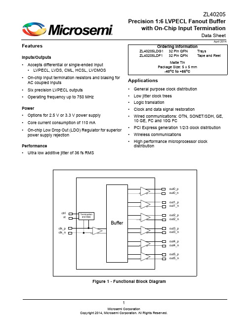
1FeaturesInputs/Outputs •Accepts differential or single-ended input •LVPECL, LVDS, CML, HCSL, LVCMOS •On-chip input termination resistors and biasing for AC coupled inputs•Six precision LVPECL outputs •Operating frequency up to 750 MHzPower •Options for 2.5 V or 3.3 V power supply •Core current consumption of 110 mA•On-chip Low Drop Out (LDO) Regulator for superior power supply rejectionPerformance •Ultra low additive jitter of 36 fs RMSApplications•General purpose clock distribution •Low jitter clock trees •Logic translation•Clock and data signal restoration•Wired communications: OTN, SONET/SDH, GE,10 GE, FC and 10G FC•PCI Express generation 1/2/3 clock distribution •Wireless communications•High performance microprocessor clock distributionApril 2014Figure 1 - Functional Block DiagramZL40205Precision 1:6 LVPECL Fanout Bufferwith On-Chip Input TerminationData SheetOrdering InformationZL40205LDG1 32 Pin QFN TraysZL40205LDF132 Pin QFNTape and ReelMatte TinPackage Size: 5 x 5 mm-40o C to +85o CTable of ContentsFeatures . . . . . . . . . . . . . . . . . . . . . . . . . . . . . . . . . . . . . . . . . . . . . . . . . . . . . . . . . . . . . . . . . . . . . . . . . . . . . . . . . 1 Inputs/Outputs . . . . . . . . . . . . . . . . . . . . . . . . . . . . . . . . . . . . . . . . . . . . . . . . . . . . . . . . . . . . . . . . . . . . . . . . .1 Power . . . . . . . . . . . . . . . . . . . . . . . . . . . . . . . . . . . . . . . . . . . . . . . . . . . . . . . . . . . . . . . . . . . . . . . . . . . . . . . .1 Performance . . . . . . . . . . . . . . . . . . . . . . . . . . . . . . . . . . . . . . . . . . . . . . . . . . . . . . . . . . . . . . . . . . . . . . . . . . .1 Applications . . . . . . . . . . . . . . . . . . . . . . . . . . . . . . . . . . . . . . . . . . . . . . . . . . . . . . . . . . . . . . . . . . . . . . . . . . . . . 1 Change Summary . . . . . . . . . . . . . . . . . . . . . . . . . . . . . . . . . . . . . . . . . . . . . . . . . . . . . . . . . . . . . . . . . . . . . . . . . 41.0 Package Description . . . . . . . . . . . . . . . . . . . . . . . . . . . . . . . . . . . . . . . . . . . . . . . . . . . . . . . . . . . . . . . . . . . .52.0 Pin Description. . . . . . . . . . . . . . . . . . . . . . . . . . . . . . . . . . . . . . . . . . . . . . . . . . . . . . . . . . . . . . . . . . . . . . . . .63.0 Functional Description . . . . . . . . . . . . . . . . . . . . . . . . . . . . . . . . . . . . . . . . . . . . . . . . . . . . . . . . . . . . . . . . . .73.1 Clock Inputs. . . . . . . . . . . . . . . . . . . . . . . . . . . . . . . . . . . . . . . . . . . . . . . . . . . . . . . . . . . . . . . . . . . . . . . . .73.2 Clock Outputs . . . . . . . . . . . . . . . . . . . . . . . . . . . . . . . . . . . . . . . . . . . . . . . . . . . . . . . . . . . . . . . . . . . . . .123.3 Device Additive Jitter. . . . . . . . . . . . . . . . . . . . . . . . . . . . . . . . . . . . . . . . . . . . . . . . . . . . . . . . . . . . . . . . .153.4 Power Supply . . . . . . . . . . . . . . . . . . . . . . . . . . . . . . . . . . . . . . . . . . . . . . . . . . . . . . . . . . . . . . . . . . . . . .163.4.1 Sensitivity to power supply noise. . . . . . . . . . . . . . . . . . . . . . . . . . . . . . . . . . . . . . . . . . . . . . . . . . .163.4.2 Power supply filtering. . . . . . . . . . . . . . . . . . . . . . . . . . . . . . . . . . . . . . . . . . . . . . . . . . . . . . . . . . . .163.4.3 PCB layout considerations. . . . . . . . . . . . . . . . . . . . . . . . . . . . . . . . . . . . . . . . . . . . . . . . . . . . . . . .164.0 AC and DC Electrical Characteristics . . . . . . . . . . . . . . . . . . . . . . . . . . . . . . . . . . . . . . . . . . . . . . . . . . . . .175.0 Performance Characterization . . . . . . . . . . . . . . . . . . . . . . . . . . . . . . . . . . . . . . . . . . . . . . . . . . . . . . . . . . .206.0 Typical Behavior . . . . . . . . . . . . . . . . . . . . . . . . . . . . . . . . . . . . . . . . . . . . . . . . . . . . . . . . . . . . . . . . . . . . . .217.0 Package Characteristics . . . . . . . . . . . . . . . . . . . . . . . . . . . . . . . . . . . . . . . . . . . . . . . . . . . . . . . . . . . . . . .238.0 Mechanical Drawing . . . . . . . . . . . . . . . . . . . . . . . . . . . . . . . . . . . . . . . . . . . . . . . . . . . . . . . . . . . . . . . . . . .24List of FiguresFigure 1 - Functional Block Diagram . . . . . . . . . . . . . . . . . . . . . . . . . . . . . . . . . . . . . . . . . . . . . . . . . . . . . . . . . . . . 1 Figure 2 - Pin Connections . . . . . . . . . . . . . . . . . . . . . . . . . . . . . . . . . . . . . . . . . . . . . . . . . . . . . . . . . . . . . . . . . . . 5 Figure 3 - Simplified Diagram of Input Stage. . . . . . . . . . . . . . . . . . . . . . . . . . . . . . . . . . . . . . . . . . . . . . . . . . . . . . 7 Figure 4 - Clock Input - LVPECL - DC Coupled. . . . . . . . . . . . . . . . . . . . . . . . . . . . . . . . . . . . . . . . . . . . . . . . . . . . 8 Figure 5 - Clock Input - LVPECL - AC Coupled. . . . . . . . . . . . . . . . . . . . . . . . . . . . . . . . . . . . . . . . . . . . . . . . . . . . 8 Figure 6 - Clock Input - LVDS - DC Coupled . . . . . . . . . . . . . . . . . . . . . . . . . . . . . . . . . . . . . . . . . . . . . . . . . . . . . . 9 Figure 7 - Clock Input - LVDS - AC Coupled . . . . . . . . . . . . . . . . . . . . . . . . . . . . . . . . . . . . . . . . . . . . . . . . . . . . . . 9 Figure 8 - Clock Input - CML- AC Coupled . . . . . . . . . . . . . . . . . . . . . . . . . . . . . . . . . . . . . . . . . . . . . . . . . . . . . . 10 Figure 9 - Clock Input - HCSL- AC Coupled . . . . . . . . . . . . . . . . . . . . . . . . . . . . . . . . . . . . . . . . . . . . . . . . . . . . . 10 Figure 10 - Clock Input - AC-coupled Single-Ended . . . . . . . . . . . . . . . . . . . . . . . . . . . . . . . . . . . . . . . . . . . . . . . 11 Figure 11 - Clock Input - DC-coupled 3.3V CMOS. . . . . . . . . . . . . . . . . . . . . . . . . . . . . . . . . . . . . . . . . . . . . . . . . 11 Figure 12 - Simplified Output Driver. . . . . . . . . . . . . . . . . . . . . . . . . . . . . . . . . . . . . . . . . . . . . . . . . . . . . . . . . . . . 12 Figure 13 - LVPECL Basic Output Termination . . . . . . . . . . . . . . . . . . . . . . . . . . . . . . . . . . . . . . . . . . . . . . . . . . . 12 Figure 14 - LVPECL Parallel Output Termination. . . . . . . . . . . . . . . . . . . . . . . . . . . . . . . . . . . . . . . . . . . . . . . . . . 13 Figure 15 - LVPECL Parallel Thevenin-Equivalent Output Termination. . . . . . . . . . . . . . . . . . . . . . . . . . . . . . . . . 13 Figure 16 - LVPECL AC Output Termination . . . . . . . . . . . . . . . . . . . . . . . . . . . . . . . . . . . . . . . . . . . . . . . . . . . . . 14 Figure 17 - LVPECL AC Output Termination for CML Inputs. . . . . . . . . . . . . . . . . . . . . . . . . . . . . . . . . . . . . . . . . 14 Figure 18 - Additive Jitter. . . . . . . . . . . . . . . . . . . . . . . . . . . . . . . . . . . . . . . . . . . . . . . . . . . . . . . . . . . . . . . . . . . . 15 Figure 19 - Decoupling Connections for Power Pins. . . . . . . . . . . . . . . . . . . . . . . . . . . . . . . . . . . . . . . . . . . . . . . 16 Figure 20 - Differential and Single-Ended Output Voltages Parameter Definitions . . . . . . . . . . . . . . . . . . . . . . . . 18 Figure 21 - Input To Output Timing . . . . . . . . . . . . . . . . . . . . . . . . . . . . . . . . . . . . . . . . . . . . . . . . . . . . . . . . . . . . 19Change SummaryPage Item Change1Applications Added PCI Express clock distribution.6Pin Description Added exposed pad to Pin Description.8Figure 4 and Figure 5Removed 22 ohm series resistors from Figure 4 and 5. These resistor are not required; however there is no impact to performance if the resistors are included.16Power supply filtering 18Figure 20Clarification of V ID and V OD .Below are the changes from the February 2013 issue to the April 2014 issue:Page Item Change8Figure 4Changed text to indicate the circuit is not recommended for VDD_driver=2.5V.Below are the changes from the November 2012 issue to the February 2013 issue:Corrected typo of 0.3 Ohm to 0.15 Ohm.1.0 Package DescriptionThe device is packaged in a 32 pin QFNFigure 2 - Pin Connections2.0 Pin DescriptionPin # Name Description3, 6clk_p, clk_n,Differential Input (Analog Input). Differential (or single ended) input signals.For all input configurations see “Clock Inputs” on page 728, 27, 26, 25, 24, 23, 18, 17, 16, 15, 14, 13out0_p, out0_nout1_p, out1_nout2_p, out2_nout3_p, out3_nout4_p, out4_nout5_p, out5_nDifferential Output (Analog Output). Differential outputs.9, 19,22, 32vdd Positive Supply Voltage. 2.5 V DC or 3.3 V DC nominal.1, 8vdd_core Positive Supply Voltage. 2.5 V DC or 3.3 V DC nominal.2, 7,20, 21gnd Ground. 0 V.4vt On-Chip Input Termination Node (Analog). Center tap between internal 50 Ohmtermination resistors.The use of this pin is detailed in section 3.1, “Clock Inputs“, for various input signal types.5ctrl Digital Control for On-Chip Input Termination (Input). Selects differential input mode;0: DC coupled LVPECL or LVDS modes1: AC coupled differential modesThis pin are internally pulled down to GND. The use of this pin is detailed in section 3.1,“Clock Inputs“, for various input signal types.10, 11,12, 29,30, 31NC No Connection. Leave unconnected.Exposed Pad Device GND.3.0 Functional DescriptionThe ZL40205 is an LVPECL clock fan out buffer with six output clock drivers capable of operating at frequencies up to 750MHz.The ZL40205 provides an internal input termination network for DC and AC coupled inputs; optional input biasing for AC coupled inputs is also provided. The ZL40205 can accept DC or AC coupled LVPECL and LVDS input signals, AC coupled CML or HCSL input signals, and single ended signals. A pin compatible device with external termination is also available.The ZL40205 is designed to fan out low-jitter reference clocks for wired or optical communications applications while adding minimal jitter to the clock signal. An internal linear power supply regulator and bulk capacitors minimize additive jitter due to power supply noise. The device operates from 2.5V+/-5% or 3.3V+/-5% supply. Its operation is guaranteed over the industrial temperature range -40°C to +85°C.The device block diagram is shown in Figure 1; its operation is described in the following sections.3.1 Clock InputsThe device has a differential input equipped with two on-chip 50 Ohm termination resistors arranged in series with a center tap. The input can accept many differential and single-ended signals with AC or DC coupling as appropriate. A control pin is available to enable internal biasing for AC coupled inputs. A block diagram of the input stage is in Figure 3.Receiverclk_n 50clk_pVt 50BiasctrlFigure 3 - Simplified Diagram of Input StageThis following figures give the components values and configuration for the various circuits compatible with the input stage and the use of the Vt and ctrl pins in each case.In the following diagrams where the ctrl pin is logically one and the Vt pin is not connected, the Vt pin can be instead connected to VDD with a capacitor. A capacitor can also help in Figure 4 between Vt and VDD. This capacitor will minimize the noise at the point between the two internal termination resistors and improve the overall performance of the device.Figure 4 - Clock Input - LVPECL - DC CoupledFigure 5 - Clock Input - LVPECL - AC CoupledFigure 6 - Clock Input - LVDS - DC CoupledFigure 7 - Clock Input - LVDS - AC CoupledFigure 8 - Clock Input - CML- AC CoupledFigure 9 - Clock Input - HCSL- AC CoupledFigure 10 - Clock Input - AC-coupled Single-EndedFigure 11 - Clock Input - DC-coupled 3.3V CMOS3.2 Clock OutputsLVPECL has a very low output impedance and a differential signal swing between 1V and 1.6 V. A simplified diagram for the output stage is shown in Figure 12.The LVPECL to LVDS output termination is not shown since there is a different device with the same inputs and LVDS outputs.out_pout_nFigure 12 - Simplified Output DriverThe methods to terminate the ZL40205 LVPECL drivers are shown in the following figures.Figure 15 - LVPECL Parallel Thevenin-Equivalent Output TerminationFigure 16 - LVPECL AC Output TerminationFigure 17 - LVPECL AC Output Termination for CML Inputs3.3 Device Additive JitterThe ZL40205 clock fanout buffer is not intended to filter clock jitter. The jitter performance of this type of device is characterized by its additive jitter. Additive jitter is the jitter the device would add to a hypothetical jitter-free clock as it passes through the device. The additive jitter of the ZL40205 is random and as such it is not correlated to the jitter of the input clock signal.The square of the resultant random RMS jitter at the output of the ZL40205 is equal to the sum of the squares of the various random RMS jitter sources including: input clock jitter; additive jitter of the buffer; and additive random jitter due to power supply noise. There may be additional deterministic jitter sources, but they are not shown in Figure 18.Figure 18 - Additive Jitter3.4 Power SupplyThis device operates employing either a 2.5V supply or 3.3V supply.3.4.1 Sensitivity to power supply noisePower supply noise from sources such as switching power supplies and high-power digital components such as FPGAs can induce additive jitter on clock buffer outputs. The ZL40205 is equipped with a low drop out (LDO) regulator and on-chip bulk capacitors to minimize additive jitter due to power supply noise. The on-chip regulation, recommended power supply filtering, and good PCB layout all work together to minimize the additive jitter from power supply noise.3.4.2 Power supply filteringJitter levels may increase when noise is present on the power pins. For optimal jitter performance, the device should be isolated from the power planes connected to its power supply pins as shown in Figure 19. •10 µF capacitors should be size 0603 or size 0805 X5R or X7R ceramic, 6.3 V minimum rating •0.1 µF capacitors should be size 0402 X5R ceramic, 6.3 V minimum rating •Capacitors should be placed next to the connected device power pins •A 0.15 Ohm resistor is recommended3.4.3 PCB layout considerationsThe power nets in Figure 19 can be implemented either as a plane island or routed power topology without changing the overall jitter performance of the device.ZL402051891922320.1 µF 0.1 µFvdd_core10 µF 0.1 µF0.15 Ωvdd0.1 µF 10 µFFigure 19 - Decoupling Connections for Power PinsAbsolute Maximum Ratings*Parameter Sym.Min.Max.Units 1Supply voltage V DD_R-0.5 4.6V 2Voltage on any digital pin V PIN-0.5VDD V 4LVPECL output current I out30mA 5Soldering temperature T260 °C 6Storage temperature T ST-55125 °C 7Junction temperature T j125 °C 8Voltage on input pin V input VDD V 9Input capacitance each pin C p500fF 4.0 AC and DC Electrical Characteristics* Exceeding these values may cause permanent damage. Functional operation under these conditions is not implied.* Voltages are with respect to ground (GND) unless otherwise statedRecommended Operating Conditions*Characteristics Sym.Min.Typ.Max.Units1Supply voltage 2.5 V mode V DD25 2.375 2.5 2.625V2Supply voltage 3.3 V mode V DD33 3.135 3.3 3.465V3Operating temperature T A-402585°C* Voltages are with respect to ground (GND) unless otherwise statedDC Electrical Characteristics - Current ConsumptionCharacteristics Sym.Min.Typ.Max.Units Notes 1Supply current LVPECL drivers -unloadedI dd_unload110mA Unloaded2Supply current LVPECL drivers - loaded (all outputs are active)I dd_load209mA Including powerto R L = 50DC Electrical Characteristics - Inputs and Outputs - for 3.3 V SupplyCharacteristics Sym.Min.Typ.Max.Units Notes1CMOS control logic high-level inputvoltageV CIH0.7*V DD V2CMOS control logic low-level inputvoltageV CIL0.3*V DD V3CMOS control logic Input leakagecurrentI IL1µA V I = V DD or 0 V4Differential input common modevoltageV CM 1.1 2.0V5Differential input voltage difference V ID0.251V6Differential input resistance V IR80100120ohm* This parameter was measured from 125 MHz to 750 MHz.* This parameter was measured from 125 MHz to 750 MHz.Figure 20 - Differential and Single-Ended Output Voltages Parameter Definitions7LVPECL output high voltage V OH V DD -1.40V 8LVPECL output low voltage V OL V DD - 1.62V 9LVPECL output differential voltage*V OD0.50.9VDC Electrical Characteristics - Inputs and Outputs - for 2.5 V SupplyCharacteristicsSym.Min.Typ.Max.Units Notes1Differential input common mode voltageV CM 1.1 1.6V 2Differential input voltage difference V ID 0.251V 3Differential input resistance V IR 80100120ohm 4LVPECL output high voltage V OH V DD -1.40V 5LVPECL output low voltage V OL V DD - 1.62V 6LVPECL output differential voltage*V OD0.40.9VDC Electrical Characteristics - Inputs and Outputs - for 3.3 V SupplyCharacteristicsSym.Min.Typ.Max.Units NotesAC Electrical Characteristics* - Inputs and Outputs (see Figure 21) - for 2.5/3.3 V supply.Characteristics Sym.Min.Typ.Max.Units Notes 1Maximum Operating Frequency1/t p750MHz2Input to output clock propagation delay t pd012ns3Output to output skew t out2out50100ps4Part to part output skew t part2part80300ps5Output clock Duty Cycle degradation t PWH/ t PWL-202Percent6LVPECL Output clock slew rate r SL0.75 1.2V/ns* Supply voltage and operating temperature are as per Recommended Operating ConditionsInputt Pt PWL t pdt PWHOutputFigure 21 - Input To Output TimingAdditive Jitter at 2.5 V*Output Frequency (MHz)Jitter MeasurementFilterTypical RMS (fs)Notes112512 kHz - 20 MHz 1392212.512 kHz - 20 MHz 1093311.0412 kHz - 20 MHz 85442512 kHz - 20 MHz 57550012 kHz - 20 MHz 506622.0812 kHz - 20 MHz 40775012 kHz - 20 MHz36Additive Jitter at 3.3 V*Output Frequency (MHz)Jitter MeasurementFilterTypical RMS (fs)Notes112512 kHz - 20 MHz 1152212.512 kHz - 20 MHz 853311.0412 kHz - 20 MHz 72442512 kHz - 20 MHz 55550012 kHz - 20 MHz 486622.0812 kHz - 20 MHz 41775012 kHz - 20 MHz395.0 Performance Characterization*The values in this table were taken with an approximate slew rate of 0.8 V/ns.*The values in this table were taken with an approximate slew rate of 0.8 V/ns.Additive Jitter from a Power Supply Tone*Carrier frequencyParameterTypicalUnitsNotes125MHz 25 mV at 100 kHz 115fs RMS 750MHz25 mV at 100 kHz59fs RMS* The values in this table are the additive periodic jitter caused by an interfering tone typically caused by a switching power supply. For this test, measurements were taken over the full temperature and voltage range for V DD = 2.5 V. The magnitude of the interfering tone is measured at the DUT.6.0 Typical BehaviorTypical Phase Noise at 622.08 MHzTypical Waveformat 155.52 MHzV OD versus FrequencyPropagation Delay versus TemperatureNote:This is for a single device. For more details see thePower Supply Tone Frequency (at 25 mV) versus PSRR at 125 MHz Power Supply Tone Frequency (at 25 mV) versus Additive Jitter at 125 MHzPower Supply Tone Magnitude (at 100 kHz) versus PSRR at 125 MHz Power Supply Tone Magnitude (at 100 kHz) versus Additive Jitter at 125 MHz7.0 Package CharacteristicsThermal DataParameter Symbol Test Condition Value UnitJunction to Ambient Thermal Resistance ΘJA Still Air1 m/s2 m/s 37.433.131.5o C/WJunction to Case Thermal Resistance ΘJC24.4o C/W Junction to Board Thermal Resistance ΘJB19.5o C/W Maximum Junction Temperature*T jmax125o C Maximum Ambient Temperature T A85o C© 2014 Microsemi Corporation. All rights reserved. Microsemi and the Microsemi logo are trademarks of Microsemi Corporation. All other trademarks and service marks are the property of their respective owners.Microsemi Corporation (NASDAQ: MSCC) offers a comprehensive portfolio of semiconductor and system solutions for communications, defense and security, aerospace and industrial markets. Products include high-performance and radiation-hardened analog mixed-signal integrated circuits, FPGAs, SoCs and ASICs; power management products; timing and synchronization devices and precise time solutions, setting the world’s standard for time; voice processing devices; RF solutions; discrete components; security technologies and scalable anti-tamper products; Power-over-Ethernet ICs and midspans; as well as custom design capabilities and services. Microsemi is headquartered in Aliso Viejo, Calif. and has approximately 3,400 employees globally. Learn more at .Microsemi Corporate Headquarters One One Enterprise, Aliso Viejo CA 92656 USA Within the USA: +1 (800) 713-4113Outside the USA: +1 (949) 380-6100Sales: +1 (949) 380-6136Fax: +1 (949) 215-4996E-mail: ***************************Information relating to products and services furnished herein by Microsemi Corporation or its subsidiaries (collectively “Microsemi”) is believed to be reliable. However, Microsemi assumes no liability for errors that may appear in this publication, or for liability otherwise arising from the application or use of any such information, product or service or for any infringement of patents or other intellectual property rights owned by third parties which may result from such application or use. Neither the supply of such information or purchase of product or service conveys any license, either express or implied, under patents or other intellectual property rights owned by Microsemi or licensed from third parties by Microsemi, whatsoever. Purchasers of products are also hereby notified that the use of product in certain ways or in combination with Microsemi, or non-Microsemi furnished goods or services may infringe patents or other intellectual property rights owned by Microsemi.This publication is issued to provide information only and (unless agreed by Microsemi in writing) may not be used, applied or reproduced for any purpose nor form part of any order or contract nor to be regarded as a representation relating to the products or services concerned. The products, their specifications, services and other information appearing in this publication are subject to change by Microsemi without notice. No warranty or guarantee express or implied is made regarding the capability, performance or suitability of any product or service. Information concerning possible methods of use is provided as a guide only and does not constitute any guarantee that such methods of use will be satisfactory in a specific piece of equipment. It is the user’s responsibility to fully determine the performance and suitability of any equipment using such information and to ensure that any publication or data used is up to date and has not been superseded. Manufacturing does not necessarily include testing of all functions or parameters. These products are not suitable for use in any medical and other products whose failure to perform may result in significant injury or death to the user. All products and materials are sold and services provided subject to Microsemi’s conditions of sale which are available on request.For more information about all Microsemi productsvisit our website at TECHNICAL DOCUMENTATION – NOT FOR RESALE。
Samsung Nanum Gothic Eco字体产品说明书

This product contains chemicals known to the State of California to cause cancer and2. The Samsung Smart Control: Press this button to mute the sound temporarily.–CC : Press and hold this button to show or hide captions on the TV's screen.MIC : Use the microphone with the Voice Recognition and Voice functions.: Turns the TV on or off.SOURCE : Displays and selects the available video sources.MENU/123: Press this button to display the On-Screen Remote. Displays the numeric buttons, the Source button, the Menu button, and other function buttons on the top of the screen so that you can run functions conveniently.–Press and hold this button to run the Voice Recognitionfunction.POINTER : Place a finger on the POINTER button and move the Samsung Smart Control. The pointer on the screen moves in the direction you moved the Samsung Smart Control. Press the POINTER button to select or run a focused item.y : Changes the volume.z : Changes the channel.< > ¡ £: Moves the focus and changes the values seen on the TV's menu.(Enter): Press this button to select or run a focused item. –Press and hold this button to launch the Guide while you are watching the TV.RETURN : Press this button to return to the previous menu. –EXIT : Press and hold this button to exit the currentlyrunning function on the TV's screen.: Use these buttons with a specific feature according to the directions on the TV's screen.EXTRA : Displays related information about the current program. SMART HUB : Press this button to bring up Smart Hub applications. (See the e-Manual chapter, "Smart Features > Smart Hub.")Pairing the TV to the Samsung Smart Control①②If your Samsung Smart Control is not paired to your TV , press and hold the buttons labeled ① and ② simultaneously for 3 seconds or more to pair the Samsung Smart Control to the TV .N The Samsung Smart Control can only be paired to one TV at a time.Using the SOURCE button to switch between video sourcesPress the SOURCE button to switch between external devices connected to the TV . For example, to switch to a game console connected to the second HDMI connector, press the SOURCE button. The Source list appears across the top of the screen. From the Source list, select HDMI2. N The connector names may differ with the product chosen.(Accessing the associated menu screen from an e-Manual topic page (Try Now): Access the associated menu item and try out the feature directly.Accessing the associated e-Manual topic from a menu screen5. Troubleshooting and MaintenanceTroubleshootingIf the TV seems to have a problem, first review this list of possible problems and solutions. Alternatively, review the Troubleshooting Section in the e-Manual. If none of the troubleshooting tips apply, visit www.samsung. com/support or call Samsung Customer Service at 1-800-SAMSUNG (1-800-726-7864).N For detailed information on troubleshooting, watch the troubleshooting videos at / spsn.N This TFT LED panel is made up of sub pixels which require sophisticated technology to produce. There may be, however, a few bright or dark pixels on the screen. These pixels will have no impact on theperformance of the product.N To keep your TV in optimum condition, upgrade to the latest software. Use the Update Now or Auto Update functions on the TV's menu (MENU > Support > Software Update > Update now or MENU > Support > Software Update > Auto Update).The TV won’t turn on.• Make sure that the AC power cord is securely plugged in to the TV and the wall outlet.• Make sure that the wall outlet is working.• Confirm that the batteries in the remote are good. If not, replace them.• Try pressing the Power button on the TV to make sure that the problem is not with the remote control. If the TV turns on, refer to “Remote control does not work” below• If the TV is connected to an antenna, check the antenna connections.• If the TV is connected to a cable/satellite box, make sure that the cable/satellite box is turned on.There is no picture/video.• Check the cable connections. Remove and reconnect all cables connected to the TV and external devices.• Set the video outputs of your external devices (Cable/satellite box, DVD, Blu-ray etc) to match the TV's input connections. For example, if an external device’s output is HDMI, connect it to an HDMI input on the TV.• Make sure that your connected devices are powered on.• Be sure to select the correct input source.• Reboot the connected device by unplugging the device's power cord and then plugging it in again.The remote control does not work.• Replace the remote control batteries. Make sure that the batteries are installed with their poles (+/–) in the correct direction.• Clean the sensor’s transmission window on the remote.• Try pointing the remote directly at the TV from 5~6 feet away.The Cable or satellite box remote control doesn’t turn the TV on or off or adjust the volume.• Program the cable or satellite box remote control to operate the TV. Refer to the Cable or satellite box user manual for the SAMSUNG TV code.Eco Sensor adjusts the brightness of the TV automatically. This feature measures the light in your room and optimizes the brightness of the TV automatically to reduce power consumption. If you want to turn this off, go to MENU > System > Eco Solution Eco Sensor.N If the screen is too dark while you are watching TV in a dark environment, it may be due to theN Do not block the sensor with any object. This can decrease picture brightness.Still image warningAvoid displaying still images (such as jpeg picture files), still image elements (such as TV channel logos, stock or news crawls at the screen bottom etc.), or programs in panorama or 4:3 image format on the screen. Ifyou constantly display still pictures, it can cause image burn-in on the LED screen and affect image quality. T reduce the risk of this adverse effect, please follow the recommendations below:。
北京联盛德微电子有限责任公司W601芯片规格书说明书

W601芯片规格书V1.0.4北京联盛德微电子有限责任公司 (Winner Micro)地址:北京市海淀区阜成路67号银都大厦18层电话:+86-10-62161900网址:文档历史目录1特征 (1)2概述 (4)3芯片特点 (4)4芯片结构 (4)5功能描述 (4)5.1SDIO设备控制器 (4)5.2高速SPI设备控制器 (5)5.3DMA控制器 (5)5.4时钟与复位 (5)5.5内存管理器 (5)5.6数字基带 (5)5.7MAC控制器 (6)5.8安全系统 (6)5.9FLASH控制器 (6)5.10RSA加密模块 (7)5.11通用硬件加密模块 (7)5.12I2C控制器 (7)5.13SAR ADC (7)5.14主/从SPI控制器 (7)5.15UART控制器 (8)5.16GPIO控制器 (8)5.17定时器 (8)5.18看门狗控制器 (8)5.19射频配置器 (8)5.20射频收发器 (8)5.21PWM控制器 (9)5.22I²S控制器 (9)5.237816/UART控制器 (9)5.24LCD控制器 (10)6管脚定义 (11)7电气特性 (14)7.1极限参数 (14)7.2射频功耗参数 (14)7.3Wi-Fi射频 (14)8封装信息 (16)1特征⚫芯片外观➢QFN68封装,7mm x 7mm⚫芯片集成度◼MCU 特性➢集成32位嵌入式Cortex-M3处理器,工作频率80MHz,内置1MB Flash,288KB RAM;➢集成3路UART 高速接口,波特率范围1200bps~2Mbps;➢集成8路10比特差分 ADC;➢集成1个SPI主从控制器,支持速率20MHz➢集成1个高速SPI从设备接口,支持最高50MHz;➢集成1个SDIO控制器,支持最高50MHz;➢集成1个I2C控制器,支持100/400Kbps 速率;➢集成GPIO控制器,支持48位可控GPIO;➢集成5路PWM接口;➢集成I2S控制器;➢集成7816接口,支持EVM2000规范,兼容串口功能;➢集成LCD控制器,最高支持4x20/8x16接口,支持2.7V~3.6V电压输出。
超微电脑 AOC-S25G-m2S 用户指南 1.0说明书

User's GuideRevision 1.0AOC-S25G-m2SUser's Guide Revision 1.0 Release Date: March 16, 2017Unless you request and receive written permission from Super Micro Computer, Inc., you may not copy any part of this document.Information in this document is subject to change without notice. Other products and companies referred to herein are trademarks or registered trademarks of their respective companies or mark holders.Copyright © 2017 by Super Micro Computer, Inc. All rights reserved.Printed in the United States of AmericaThe information in this User's Guide has been carefully reviewed and is believed to be accurate. The vendor assumes no responsibility for any inaccuracies that may be contained in this document, and makes no commitment to update or to keep current the information in this user's guide, or to notify any person or organization of the updates. Please Note: For the most up-to-date version of this user's guide, please see our Website at .Super Micro Computer, Inc. ("Supermicro") reserves the right to make changes to the product described in this user's guide at any time and without notice. This product, including software and documentation, is the property of Supermicro and/or its licensors, and is supplied only under a license. Any use or reproduction of this product is not allowed, except as expressly permitted by the terms of said license.IN NO EVENT WILL SUPER MICRO COMPUTER, INC. BE LIABLE FOR DIRECT, INDIRECT, SPECIAL, INCIDENTAL, SPECULATIVE OR CONSEQUENTIAL DAMAGES ARISING FROM THE USE OR INABILITY TO USE THIS PRODUCT OR DOCUMENTATION, EVEN IF ADVISED OF THE POSSIBILITY OF SUCH DAMAGES. IN PARTICULAR, SUPER MICRO COMPUTER, INC. SHALL NOT HAVE LIABILITY FOR ANY HARDWARE, SOFTWARE, OR DATA STORED OR USED WITH THE PRODUCT, INCLUDING THE COSTS OF REPAIRING, REPLACING, INTEGRATING, INSTALLING OR RECOVERING SUCH HARDWARE, SOFTWARE, OR DATA.Any disputes arising between the manufacturer and the customer shall be governed by the laws of Santa Clara County in the State of California, USA. The State of California, County of Santa Clara shall be the exclusive venue for the resolution of any such disputes. Supermicro's total liability for all claims will not exceed the price paid for the hardware product.FCC Statement: This equipment has been tested and found to comply with the limits for a Class A digital device pursuant to Part 15 of the FCC Rules. These limits are designed to provide reasonable protection against harmful interference when the equipment is operated in a commercial environment. This equipment generates, uses, and can radiate radio frequency energy and, if not installed and used in accordance with the manufacturer’s instruction manual, may cause harmful interference with radio communications. Operation of this equipment in a residential area is likely to cause harmful interference, in which case you will be required to correct the interference at your own expense.California Best Management Practices Regulations for Perchlorate Materials: This Perchlorate warning applies only to products containing CR (Manganese Dioxide) Lithium coin cells. “Perchlorate Material-special handling may apply. See /hazardouswaste/perchlorate”.WARNING: Handling of lead solder materials used in this product may expose you to lead, a chemical known to the State of California to cause birth defects and other reproductive harm.PrefacePrefaceAbout this User's GuideThis user's guide is written for system integrators, IT technicians and knowledgeable end users. It provides information for the installation and use of the AOC-S25G-m2S add-on card.About this Add-on CardThe Supermicro AOC-S25G-m2S is a leading edge 25GbE controller. Based on the Mellanox ConnectX®-4 Lx EN chipset with features such as VXLAN and NVGRE, it is backward compatible with 10GbE networks and addresses bandwidth demand from virtualized infrastructures in data centers or cloud deployments. It supports the RoCE specification with CPU offload, delivering low-latency and high-performance over Ethernet networks. Supermicro® Asset Management and thermal detection give an extra layer of controller health management and peace of mind. The Supermicro AOC-S25G-m2S high performance 25GbE adapter solution is an excel-lent choice to enhance network connectivity in data centers and enterprise environ-ments. For more information regarding product support or updates, please refer to our website at /products/nfo/networking.cfm#adapter.An Important Note to the UserAll images and layouts shown in this user's guide are based upon the latest PCB Revision available at the time of publishing. The card you have received may or may not look exactly the same as the graphics shown in this user's guide.Returning Merchandise for ServiceA receipt or copy of your invoice marked with the date of purchase is required beforeany warranty service will be rendered. You can obtain service by calling your ven-dor for a Returned Merchandise Authorization (RMA) number. When returning the motherboard to the manufacturer, the RMA number should be prominently displayed on the outside of the shipping carton, and the shipping package is mailed prepaid or hand-carried. Shipping and handling charges will be applied for all orders that must be mailed when service is complete. For faster service, you can also requesta RMA authorization online (/RmaForm/).This warranty only covers normal consumer use and does not cover damages in-curred in shipping or from failure due to the alternation, misuse, abuse or improper maintenance of products.During the warranty period, contact your distributor first for any product problems.Conventions Used in the User's GuidePay special attention to the following symbols for proper system installation and to prevent damage to the system or injury to yourself:Warning: Important information given to ensure proper system installationor to prevent damage to the components or injury to yourself.Note: Additional information given to differentiate between various modelsor provides information for correct system setup.Naming ConventionSMC Networking Add-on Cards Preface–1 –234 –56 7Character Representation Options1st Product Family AOC: Add On Card2nd Form Factor S: Standard, P: Proprietary, C: MicroLP, U: UIO3rd Product Type/Speed G: GbE (1Gb/s), TG: 10GbE (10Gb/s), 40G: 40GbE(40Gb/s), IBF: FDR IB (56Gb/s), IBQ: QDR IB (40Gb/s) 4th Chipset Model (Optional)N: Niantec (82599), P: Powerville (i350),S: Sageville (X550), F: Fortville (XL710)5th Chipset Manufacturer i: Intel, m: Mellanox, b: Broadcom6th Number of Ports1: 1 port, 2: 2 ports, 4: 4 ports7th Connector Type (Optional)S: SFP+, T: 10GBase-T, Q: QSFP+, C: QSFP28Contacting SupermicroHeadquartersAddress:Super Micro Computer, Inc.980 Rock Ave.San Jose, CA 95131 U.S.A.Tel:+1 (408) 503-8000Fax:+1 (408) 503-8008Email:************************(GeneralInformation)**********************(TechnicalSupport) Website:EuropeAddress:Super Micro Computer B.V.Het Sterrenbeeld 28, 5215 ML's-Hertogenbosch, The NetherlandsTel:+31 (0) 73-6400390Fax:+31 (0) 73-6416525Email:*******************(GeneralInformation)*********************(TechnicalSupport)*****************(CustomerSupport) Website:www.supermicro.nlAsia-PacificAddress:Super Micro Computer, Inc.3F, No. 150, Jian 1st Rd.Zhonghe Dist., New Taipei City 235Taiwan (R.O.C)Tel:+886-(2) 8226-3990Fax:+886-(2) 8226-3992Email:**********************.twWebsite:PrefaceTable of ContentsPrefaceChapter 1 Overview1-1 Overview .........................................................................................................1-1 1-2 Key Features ...................................................................................................1-1 1-3 Specifications ..................................................................................................1-2 General ............................................................................................................1-2 Host Interface ..................................................................................................1-2 Networking Features .......................................................................................1-2 CPU Offload Features.....................................................................................1-3 Overlay Networks ............................................................................................1-3 Hardware-Based I/O Virtualization ..................................................................1-3 Storage Offloads .............................................................................................1-3 Management Features ....................................................................................1-3 Virtualization Features.....................................................................................1-4 Operating System Support ..............................................................................1-4 Remote Boot ...................................................................................................1-4 Operating Conditions ......................................................................................1-4 Physical Dimensions .......................................................................................1-5 Weight .............................................................................................................1-5 Supported Platforms .......................................................................................1-5 Compliance/Environmental .............................................................................1-5 1-4 Similar Products ..............................................................................................1-6 1-5 Optional Parts List ...........................................................................................1-6 Chapter 2 Hardware Components2-1 Add-On Card Image and Layout .....................................................................2-1 2-2 Major Components ..........................................................................................2-2 2-3 SFP28 Ethernet Connections..........................................................................2-3 2-4 NC-SI Header & PCI-E 3.0 x8 Golden Finger ................................................2-4 Chapter 3 Installation3-1 Static-Sensitive Devices ..................................................................................3-1 3-2 Before Installation ...........................................................................................3-2 3-3 Installing the Add-on Card ..............................................................................3-2 3-4 Installing Drivers from the CD-ROM CDR-NIC ...............................................3-3 Windows Drivers .............................................................................................3-4 3-5 Installing Drivers ............................................................................................3-4 Linux Drivers ...................................................................................................3-4 Firmware Update Procedures .........................................................................3-5NotesChapter 1: OverviewChapter 1Overview1-1 OverviewCongratulations on purchasing your add-on card from an acknowledged leader in the industry. Supermicro products are designed with the utmost attention to detail to provide you with the highest standards in quality and performance. For product support and updates, please refer to our website at / products/nfo/networking.cfm#adapter.1-2 Key FeaturesThe key features of this add-on card include the following:• Dual SFP28 Connectors• Low-Profile, Short Length Standard Form Factor• PCI-E 3.0 x8• Mellanox ConnectX®-4 Lx EN Ethernet Controller• Asset Management Features with thermal sensor• Hardware offloads for VXLAN, NVGRE and GENEVE encapsulated traffic • Low latency RDMA over Converged Ethernet (RoCE)• PCI-SIG SR-IOV compliant• Jumbo Frames support up to 9.6kB• PXE support• Erasure Coding Offload• NC-SI for IPMI support• RoHS compliant 6/61-3 SpecificationsGeneral• Mellanox ConnectX®-4 Lx EN dual-port 25Gbps controller • Compact size low-profile standard form factor• PCI-E 3.0 x8 (8GT/s, 5GT/s or 2.5GT/s) interface • Dual SFP28 connectors• Typical power consumption: 8.7WHost Interface• PCI-E 3.0 x8• Message Signal Interrupt (MSI-X)Networking Features• 25G Ethernet Consortium 25 Gigabit Ethernet• IEEE 802.3ae 10 Gigabit Ethernet• IEEE 802.3az Energy Efficient Ethernet• IEEE 802.3ap based auto-negotiation and KR startup • IEEE 802.ad, 802.1AX Link Aggregation• IEEE 802.1Q, 802.1p VLAN tags and priority• IEEE 802.1Qau (QCN) – Congestion Notification • IEEE 802.1Qaz (ETS)• IEEE 802.1Qbb (PFC)• IEEE 802.1Qbg• IEEE 1588v2Chapter 1: Overview • Jumbo frame support (9.6KB)CPU Offload Features• RDMA over Converged Ethernet (RoCE)• TCP/UDP/IP stateless offload• LSO, LRO, checksum offload• RSS, TSS, HDS, VLAN insertion/stripping. Receive flow steering• Intelligent interrupt coalescenceOverlay Networks• Stateless offloads for overlay networks and tunneling protocols• Hardware offload of encapsulation and decapsulation of NVGRE and VXLAN overlay networksHardware-Based I/O Virtualization• Single Root IOV• Multi-function per port• Address translation and protection• Multiple queues per virtual machine• Enhanced QoS for vNICs• VMware NetQueue supportStorage Offloads• RAID offload – erasure coding (Reed-Solomon) offloadManagement Features• Asset Management features with thermal sensor• NC-SI for IPMI SupportVirtualization Features• SR-IOV: up to 256 Virtual Functions• SR-IOV: up to 16 Physical Functions per port• 1K ingress and egress QoS levels• Guaranteed QoS for VMsOperating System Support• RHEL/CentOS• Windows• FreeBSD• VMware• OpenFabrics Enterprise Distribution (OFED)• OpenFabrics Windows Distribution (WinOF-2)Remote Boot• Remote boot over iSCSi• PXE and UEFIOperating Conditions• Operating temperature: 0°C to 55°C (32°F to 131°F)• Storage temperature: -40°C to 70°C (-40°F to 158°F)• Storage humidity: 90% non-condensing relative humidity at 35°CChapter 1: Overview Physical Dimensions• Card PCB dimensions: 14.2cm x 6.89cm (5.6in x 2.71in) (LxW)• Height of end brackets: standard – 12cm (4.725in), low-profile – 8cm (3.15in)Weight• 89.58g (0.1975lb)Supported Platforms• Motherboards with minimum PCI-E 3.0 x8 expansion slot• Server Systems with low-profile or full-height PCI-E 3.0 x8 expansion slots • NC-SI feature is only supported by Supermicro® motherboards with correspond-ing NC-SI connectorsNote: This product is intended to be used with Supermicro server systemsor motherboards as an integrated solution package.Compliance/Environmental•RoHS Compliant 6/6, Pb Free1-4 Similar Products1-5 Optional Parts ListChapter 2: Hardware ComponentsChapter 2Hardware Components2-1 Add-On Card Image and LayoutThe AOC-S25G-m2S LayoutThe AOC-S25G-m2S Image1. Mellanox ConnectX®-4 Lx EN 5. SFP28 Port2 Link LED2. SFP28 Port1 6. NC-SI header3. SFP28 Port27. PCI-E 3.0 x84. SFP28 Port1 Link LED12345672-2 Major ComponentsThe following major components are installed on the AOC-S25G-m2S:1. Mellanox ConnectX®-4 Lx EN Controller2. Dual SFP28 (Small Form Factor Pluggable) Ports3. Two (2) SFP28 Link/Activity LED Indicators4. NC-SI for IPMI supportChapter 2: Hardware Components1. SFP1: SFP28 Port12. SFP2: SFP28 Port23. SFP28 Port1 Link LED4. SFP28 Port1 Link LED2-3 SFP28 Ethernet ConnectionsSFP28 (SFP1/SFP2) ConnectorsTwo small form-factor pluggable (SFP28) optical transceiver connectors (SFP1/SFP2) are located on the add-on card. These SFP28 ports provide Ethernet up to 25GbE network connections. See the layout below for the locations.SFP28 (SFP1/SFP2) Link/Activity LED IndicatorsTwo LAN Link/Activity LED indicators are located at PORT1 LED and PORT2 LED on the add-on card. PORT1 LED is used for the SFP28 SFP1 connector, and PORT2 LED, for SFP28 SFP2 connector. See the table below for the LED states.2-4 NC-SI Header & PCI-E 3.0 x8 Golden FingerNC-SI HeaderA Network-Controller Sideband Interface (NC-SI) header is located at JNCSI1 on the add-on card. Connect an appropriate cable from this header to a motherboard to provide the out-of-band (sideband) connection between the onboard Baseboard Management Controller (BMC) and a Network Interface Controller (NIC) for remote management. For the network sideband interface to work properly, you will need to use a motherboard that supports NC-SI and also need to have a special cable. Please contact Supermicro at to purchase the cable for this header. See the layout below for the location of the JNCSI1 header.PCI-E 3.0 x8 Golden FingerA PCI-E 3.0 x8 Golden Finger is located at JGF1 on the add-on card. Insert this connector into a PCI-E 3.0 x8 slot on a motherboard to use this add-on card. See the layout below for the location.1. NS-CI Header2. PCI-E3.0 x8 Golden FingerChapter 3: InstallationChapter 3Installation3-1 Static-Sensitive DevicesElectrostatic Discharge (ESD) can damage electronic com p onents. To avoid dam-aging your add-on card, it is important to handle it very carefully. The following measures are generally sufficient to protect your equipment from ESD.Precautions• Use a grounded wrist strap designed to prevent static discharge.• Touch a grounded metal object before removing the add-on card from the antistatic bag.• Handle the add-on card by its edges only; do not touch its components, or peripheral chips.• Put the add-on card back into the antistatic bags when not in use.• For grounding purposes, make sure that your system chassis provides excellent conductivity between the power supply, the case, the mounting fasteners and the add-on card.UnpackingThe add-on card is shipped in antistatic packaging to avoid static damage. When unpacking your component or your system, make sure that the person handling it is static protected.Warning: To avoid damaging your components and to ensure properinstallation, be sure to always connect the power cord last, and alwaysremove it before adding, removing or changing any hardware components.3-2 Before InstallationTo install the add-on card properly, be sure to follow the instructions below.1. Power down the system.2. Unplug the power cord.3. Use industry standard anti-static equipment (such as gloves or wrist strap)and follow the precautions on Page 3-1 to avoid damage caused by ESD.4. Familiarize yourself with the server, motherboard, and/or chassis documenta-tion.5. Confirm that your operating system includes the latest updates and hotfixes.3-3 Installing the Add-on CardFollow the steps below to install the add-on card into your system.1. Remove the server cover and, if any, set aside any screws for later use.2. Remove the add-on card slot cover. If the case requires a screw, place thescrew aside for later use.3. Position the add-on card in the slot directly over the connector, and gentlypush down on both sides of the card until it slides into the PCI connector.4. Secure the add-on card to the chassis. If required, use the screw that youpreviously removed.5. Attach any necessary external cables to the add-on card.6. Replace the chassis cover.7. Plug the power cord into the wall socket and power up the system.Chapter 3: InstallationNote: If the FOUND NEW HARDWARE WIZARD screen displays on yoursystem, click CANCEL.3. Click on INSTALL DRIVERS AND SOFTWARE.4. The Install Shield Wizard will start .Follow the prompts to complete the instal-lation.3-4 Installing Drivers from the CD-ROM CDR-NICFollow the steps below to install the drivers needed for your Windows OS support. The controller comes with a driver on the CD-ROM CDR-NIC.1. Run the CDR-NIC. (If you do not have a product CD-ROM, download driversfrom the Supermicro Support Website and then transfer them to your system.)2. When the SUPERMICRO window appears, click on the computer icon next tothe product model.3-5 Installing DriversUse the procedures below to install drivers for the AOC-S25G-m2S add-on card for both Linux and Windows.Linux DriversUse the following procedures to install drivers on the Linux operating system.Installing 25G Drivers for the Linux Operating System1. From the CDR-NIC LAN driver CD, go to the following directory: Mellanox> Linux. You may also go to the Supermicro FTP site at ftp://ftp.super-/Networking_Drivers/CDR-NIC_1.50_for_Add-on_NIC_Cards/Mellanox/25GbE/Linux/.2. Download the Linux driver package file.3. Install the driver by entering the following commands:tar xzvf mlnx-en–<ver>.tgzcd mlnx-en–<ver>./install.shThis installs the Linux drivers to your system.Note: Driver installation may require root privileges.Windows DriversUse the following procedures to install drivers on the Windows operating system.Installing 25G Drivers for the Windows Operating System1. From the CDR-NIC LAN driver CD, go to the following directory: Mellanox> Windows. You may also go to the Supermicro FTP site at ftp://ftp.super-/Networking_Drivers/CDR-NIC_1.50_for_Add-on_NIC_Cards/Mellanox/25GbE/Windows/.2. Choose the desired Windows driver package file.3. Double -click to run and install the executable (.exe ) file in the driver pack-age.4. The Install Shield Wizard will start .Follow the prompts to complete the instal-lation.Chapter 3: InstallationFirmware Update ProceduresUse the following procedures for updating the AOC-S25G-m2S add-on card firm-ware for both the Linux and Windows operating systems.Updating Firmware for the Linux Operating System1. From the CDR-NIC LAN driver CD, go to the following directory: MellanoxFirmware_Tool > Linux. You may also go to the Supermicro FTP site at ftp:// /Networking_Drivers/CDR-NIC_1.50_for_Add-on_NIC_Cards/Mellanox/Firmware_Tool/Linux/.2. Choose the MFT Linux package file and untar the package file.3. Install the package by entering the following command:cd mft–<ver>./install.sh4. Install the firmware by the following commands:mst startmst status *write down the pci_cr0 device name*flint –d <pci_cr0 device name> –i <firmware file name>.bin burnUpdating Firmware for the Windows Operating System1. From the CDR-NIC LAN driver CD, go to the following directory: MellanoxFirmware_Tool > Linux. You may also go to the Supermicro FTP site at ftp:// /Networking_Drivers/CDR-NIC_1.50_for_Add-on_NIC_Cards/Mellanox/Firmware_Tool/Windows/.2. Choose the desired MFT Windows package file.3. Double-click to run and install the MFT package file.4. Open the DOS command prompt and locate the MFT folder.5. Install the firmware by entering the following commands:mst startmst status *write down the pci_cr0 device name*flint –d <pci_cr0 device name> –i <firmware file name>.bin burn(Disclaimer Continued)The products sold by Supermicro are not intended for and will not be used in life support systems, medical equipment, nuclear facilities or systems, aircraft, aircraft devices, aircraft/emergency com-munication devices or other critical systems whose failure to perform be reasonably expected to result in significant injury or loss of life or catastrophic property damage. Accordingly, Supermicro disclaims any and all liability, and should buyer use or sell such products for use in such ultra-hazardous ap-plications, it does so entirely at its own risk. Furthermore, buyer agrees to fully indemnify, defend and hold Supermicro harmless for and against any and all claims, demands, actions, litigation, and proceedings of any kind arising out of or related to such ultra-hazardous use or sale.。
IO-Link数字流量开关操作手册说明书

Before UseDigital Flow SwitchPF3A703H/PF3A706H/PF3A712H-LSafety InstructionsThese safety instructions are intended to prevent hazardous situations and/orequipment damage.These instructions indicate the level of potential hazard with the labels of"Caution", "Warning" or "Danger". They are all important notes for safety and mustbe followed in addition to International standards (ISO/IEC) and other safetyregulations.OperatorThank you for purchasing an SMC PF3A703H/PF3A706H/PF3A712H-L DigitalFlow Switch.Please read this manual carefully before operating the product and make sure youunderstand its capabilities and limitations. Please keep this manual handy forfuture reference.Safety Instructions1324DisplayBody(IN side)Connector pin numbers(on the product)Mounting•Never mount the product in a place that will be used as a mechanical support during piping.•Never mount the product upside down.•Attach the piping so that the fluid flows in the direction indicated by the arrow on the body.•The monitor with integrated display can be rotated.Rotating the display with excessive force will damage the end stop.•Visibility decreases if the display is viewed from the opposite side to the buttons.Check the settings and display from in front of the display.Mounting and InstallationRefer to the product catalogue or SMC website (URL https://) for moredetailed information.IN OUTArrowthe IN side of the product.When installing a regulator at the IN side of the product, make sure that hunting is not generated.•The piping on the IN side must have a straight section of piping whose length is 8 timesthe piping diameter or more.If a straight section of piping is not installed, the accuracy will vary by approximately 3%F.S.•Avoid sudden changes to the pipingsize on the IN side of the product.The accuracy may vary.•Do not release the OUT side pipingport of the product directly to theThe accuracy may vary.○Flow direction○Rotation of the display•Use the correct tightening torque for piping. (Refer to the table below for the requiredtorque values.)•If the tightening torque is exceeded, the product can be damaged.If the tightening torque is insufficient, the fittings may become loose.•Avoid any sealing tape getting inside the fluid passage.•Ensure there is no leakage after piping.•When mounting the fitting, a spanner should be used on the body (metal part) of thefitting only.Holding other parts of the product with a spanner may damage the product.Specifically, make sure that the spanner does not damage the M12 connector.■WiringConnection•Connections should only be made with the power supply turned off.•Use a separate route for the product wiring and any power or high voltage wiring. If wiresand cables are routed together with power or high voltage cables, malfunction may resultdue to noise.•If a commercially available switching power supply is used, be sure to ground the frameground (FG) terminal. If the product is connected to the commercially available switchingpower supply, switching noise will be superimposed and the product specifications will notbe satisfied. In that case, insert a noise filter such as a line noise filter/ ferrite between theswitching power supplies or change the switching power supply to the series power supply.Connecting/Disconnecting•Align the lead wire connector with the connector keygroove, and insert it straight in. Turn the knurled partclockwise. Connection is complete when the knurledpart is fully tightened. Check that the connection is notloose.•To remove the connector, loosen the knurled part andpull the connector straight out.Connector pin numbers (lead wire)Outline of SettingsPower is supplied.∗: If a button operation is not performed for 3 seconds during the setting, the display will flash. (This is toprevent the setting from remaining incomplete if, for instance, an operator were to leave during setting.)∗: 3 step setting mode, simple setting mode and function selection mode settings will reflect on each other.■3 step setting modeIn the3 step setting mode, the set value selected in the sub display and the hysteresiscan be changed in just 3 steps.Switch ONP_1Flow[L/min]H_1settingsWhen shipped, the default setting is as follows.When the flow exceeds the set value [P_1], the switch will be turned ON.When the flow falls below the set value by the amount of hysteresis [H_1] or more, theswitch will turn OFF.If the operation shown below is acceptable, then keep these settings.For more detailed settings, set each function in the function selection mode.(1) Press the S button once when the item to be changed is displayed on the subdisplay.The set value on the sub display (right) will start flashing.S<Operation>[Hysteresis mode]In the 3 step setting mode, the set value (P_1 or n_1) and hysteresis (H_1) can bechanged.Set the items on the sub display (set value and hysteresis) using the ▲ or ▼ buttons.When changing the set value, follow the operation below. The hysteresis setting can bechanged in the same way.(2) Press the ▲ or ▼ button to change the set value.The ▲ button is to increase and the ▼ button is to decrease the set value.●Press the ▲ button once to increase the value by one digit, press and hold tocontinuously increase.●When ▲ and ▼ buttons are pressed simultaneously for 1 second or more, the setvalue is displayed as [ - - - ], and the set value will be set to the same as thedisplayed value automatically. Afterwards, it is possible to adjust the value bypressing ▲ or ▼.●Press the ▼ button once to reduce the value by one digit, press and hold tocontinuously reduce.(3) Press the S button to complete the setting.To change setting, refer to the operation manual from SMC website(URL https://) or contact SMC.<Operation>[Hysteresis mode](1) Press the S button for 1 second or longer(but less than 3 seconds) in measurementmode. [SEt] is displayed on the main display.When the button is released while in the [SEt] display, the current flow value isdisplayed on the main display, [P_1] or [n_1] is displayed on the sub display (left)and the set value is displayed on the sub display (right).(2) Change the set value using the ▲ or ▼ button, and press the SET button to set thevalue. Then, the setting moves to hysteresis setting.(5) Press and hold the S button for 2 seconds or longer to complete the simple setting.(If the button is pressed for less than 2 seconds, the setting will be returned to P_1.)(3) Change the set value with the ▲ or ▼ button, and press the S button to set thevalue. Then, the setting moves to the setting of OUT2.∗1: Selected items of (1) to (4) become valid after pressing the S button.∗2: After enabling the setting by pressing the S button, it is possible to return to measurementmode by pressing the S button for 2 seconds or longer.∗3: When the output mode is set to accumulated pulse, error output or output OFF, the simplesetting mode cannot be used.(the setting returns to measurement mode by releasing the button when [SEt] is displayed.)■Simple setting modeIn the simple setting mode, the set value, hysteresis and delay time can be changed whilechecking the current flow value (main display).(4) Like the setting of OUT1, the setting returns to the setting of OUT2 by pressing theS button after setting the set value and hysteresis.∗: When [F 1] and [F 2] are set to accumulatedpulse output, error output or output OFF [---]will be displayed in the sub screen when[SEt] is displayed. It is not possible to moveto the Simple setting mode.Change the Function Settings∗1: Setting is only possible for models with the units selection function.∗2: [F 2] The OUT2 setting can be set on the product screen, but since there is no OUT2 switch outputfunction as an output specification, it is not possible to output the ON/OFF signal to an external device.∗3: When the 1 switch output type (output specification symbol is L) is used, [F5] is displayed as [---]and cannot be set.1 to 5 V or 0 to 10 V can be selected when the analogue voltage output type is used.Analogue output free range function can be selected.∗4: When Line name is selected, a suitable line name can be input.To change setting, refer to the operation manual from SMC website(URL https://) or contact SMC.■Function selection modeIn measurement mode, press theS button for 3 seconds or longer,to display [F 0].The [F] indicates the mode forchanging each Function Setting.Press the S button for 2 secondsor longer in function selectionmode to return to measurementmode.To change setting, refer to the operation manual from SMC website(URL https://) or contact SMC.○Reset operationThe Accumulated Flow, Peak Value and Bottom Value can be reset.To reset the accumulated value, press the ▼ and S button for 1 second or longer.○Snap shot functionThe current flow rate value can be stored to the switch output ON/OFF set point.When the items on the Sub display (left) are selected in either 3 step setting mode, Simplesetting mode or Setting of each function mode, by pressing the ▲ and ▼ buttonssimultaneously for 1 second or longer, the value of the sub display (right) will show "----",and the values corresponding to the current flow rate are automatically displayed.MaintenanceHow to reset the product after a power loss or when the power has beenunexpectedly removedThe settings for the product are retained in memory prior to the power loss or de-energizingof the product.The output condition is also recoverable to that prior to the power loss or de-energizing.However, this may change depending on the operating environment. Therefore, check thesafety of the whole installation before operating the product.If the installation is using accurate control, wait until the product has warmed up(approximately 10 to 15 minutes) before operation.Refer to the product catalogue or operation manual from SMC website(URL https://) for more information about the product specifications anddimensions.Specifications / Dimensions○Key-lock function(1) Press the S button for 5 seconds or longer in measurement mode. When [oPE] isdisplayed on the main display, release the button.The current setting "LoC" or "UnLoC" will be displayed on the sub display.(2) Select the key locking/un-locking using the ▲ or ▼ button, and press the S button toset.To use each of these functions, refer to the operation manual from SMC website(URL https://) or contact SMC.The IODD file can be downloaded from the SMC website (URL https://).Note: Specifications are subject to change without prior notice and any obligation on the part of the manufacturer.© 2020 SMC Corporation All Rights ReservedAkihabara UDX 15F, 4-14-1, Sotokanda, Chiyoda-ku, Tokyo 101-0021, JAPANPhone: +81 3-5207-8249 Fax: +81 3-5298-5362URL https://PF※※-OMX0003Troubleshootingdisplayed, please contact SMC.Refer to the operation manual from SMC website (URL https://) for moreinformation about troubleshooting.。
AXR-202SSD用户指南说明书
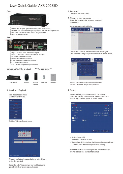
User Quick Guide AXR-202SSD1.PasswordThe initial password is 1234.2.Changing your passwordPlease change your initial password to protect your privacy.Menu->Account->AdministratorIf you click mouse on the keyboard in the above gure,a screen for entering the password appears as shown below.Enter a new password, enter it one more time, and click Apply to change your password.3.Search and PlaybackFrom the right-click menu Click the "Search" menu.Click the "Calendar Search" menu.The date marked on the calendar in red is the date on which it is recorded.Select the date / time / minute you want to play and press Play button to start playback screen.4.BackupAfter connecting the USB memory stick to the DVR,select the "Backup" menu from the right-click menu and the backup menu will appear as shown below.-Device: Select USB.-File format: Select AVI or HAV.-Time setting: Set the backup start time and backup end time.-Channel: Check the channel you want to back up.Click the "Backup" button to proceed with the backup.Do not operate the DVR during backup.FrontRearComponents of the product ① Power LED : It lights green when the power is turned on.② Record LED : When recording is in progress, the indicator lights in red.③ Alarm LED : When an alarm occurs, it lights yellow.④ Remote control receiver① Input cameras : Enter the camera signal.② Sensor / Alarm I / O and RS-485 output terminal ③ HD monitor output terminal ④ Network connection terminal⑤ USB memory and mouse connector ⑥ DC 12V output terminalDC 12V adaptor power input terminalmain body MouseRemote controlConnectorManual*** No SSD Drive ***work monitoring (CMS program)CMS (Central Management Software) is an integrated management program that efficiently manages multiple DVRs over the network.It provides real-time image monitoring, search- i ng and backup of stored images, and setting f unction. Up to 256 channels of live video can be monitored simultaneously.Run the CMS_Ver X.X.X_Setup.exe file (available on the Internet: -> Support -> Downloads).The CMS icon is created on the desktop.①Feature selection: Live S, Live M, Search, Playback, Backup, E-Map, Info,DVR Settings, PC Settings.②Video surveillance screen: It shows video of DVR.③Connection list management window: You can add, modify and delete groups and DVRs.④Screen selection: Select the channel to be displayed on the video display window or select the screen configuration.⑤Control function or calendar display window: In Live S and Live M mode, PTZ, Preset,remote port control, and video adjustment are available. In playback and backup mode,the calendar is displayed.● Live M : This mode controls multiple DVRs. Up to 256 channels can be managed as 4 pages of 64 channels each.Enter the DVR information in the same way as Live S and add it to the list. To connect, double-click theGroup name or click the right mouse button on the pop-up menu to connect to all the DVRs belonging to the group.● Search : Without a separate program, you can search directly by pressing the search button and then selecting the desired DVR.< Search screen >● Live S : It is a mode to control one DVR. After running CMS, position the mouse cursor on My Group in thetop right of the screen and click Add DVR among the popup menu that appears when you right-click to enter the information of the DVR you want to connect. Enter a name in the Name field and a DDNS address in the address field.You can enter the base address based on the MAC address (ex ) or the address set by the user (ex. ).Enter the port number in the Fortran. Enter admin in the User field and 1234 in the Password field.Of course, the user and password can be added or changed in the DVR menu. After selecting the number of channels and pressing the OK button, the DVR entered in My Group will be added. To connect, double-click the added name or click the right mouse button on the pop-up menu.7.Mobile7-1. Android PhoneIf you press the menu button on the smartphone, the DVR list related menu pops up at the bottom.add, edit, delete and exit buttons.Click ADD button to enter DVR information and press OK button to add it to the list.Enter the desired name in the name, and enter the connection address in the domain.You can enter a base address based on the MAC address (for example, ) or a user-defined address (for example, ).Enter the port number for the port.Enter the ID for admin and the password for 1234.ID and password can be added and changed in DVR menu.Select the DVR to connect from the list and press the Connect button to connect to DVR. Multi-channel live monitoring, PTZ control, search and multi-channel playback (audio support), relay remote control, stream type selection,aspect ratio selection.Calendar search function provides fast and cool searchThere is recorded data in red color.First, select the date you want to search in the calendar, select the time in the time bar, Afterselecting the minutes, press the OK button and the playback screen will appear as shown on the right.Screen split selection: Select the split screen to be displayed on the video display window.Reverse playback: Reverse play button.Forward playback: Forward playback button.Pause: Pause button.Slow playback: Slow playback button.(x1/4, x1/2 speed)Fast playback: Fast playback button.This app is for smartphones. Supports iPhone, iPAD, Android smartphone.(Application Name: Direct Viewer (Android), Direct Watch (iOS))Install and run the application.① ② ③ ④ ⑤⑥⑥5.Setting up your network5-1. Checking the connection address and port number5-2. Connecting to the networkMenu->Network->DDNSMenu->Network->TCP/IPAs shown in the figure above, the address shown in the default value is the connection address of the DVR.(For example, )Enter the DVR connection address and port number in the Internet address window as shown in the following example and press the enter key.Example: :80After installing ActiveX, the above screen appears.If you enter your ID and password, you can see the video.(The default setting is user: admin, password: 1234.)● Precautions :Construction of this product requires experience and skill, so it should be done by a specialist. Personal construction may cause fire, electric shock or breakdown. For installation and installation, p lease contact our headquarters or your dealer.The contents of this manual may be changed depending on the upgrade of the product. The specifications and appearance of the product are subject to change without notice in order to improve the quality.Since the SSD storage device is a consumable item, please check the status of the SSD storage device at least once a week through playback and search.*** Supportable SSD Drive type -> M.2 SSD Drive。