LM224ADRE4中文资料
LM224DT中文资料

VOL
Low Level Output Voltage (R L = 10kΩ) o Tamb = +25 C Tmin. ≤ Tamb ≤ Tmax. Slew Rate VCC = 15V, VI = 0.5 to 3V, RL = 2kΩ, C L = 100pF, unity gain) Gain Bandwidth Product VCC = 30V, f = 100kHz, Vin = 10mV RL = 2kΩ, CL = 100pF Total Harmonic Distortion f = 1kHz, AV = 20dB, RL = 2kΩ, VO = 2Vpp CL = 100pF, VCC = 30V Equivalent Input Noise Voltage f = 1kHz, Rs = 100Ω, VCC = 30V Input Offset Voltage Drift Input Offset Current Drift Channel Separation (note 5) 1kHz ≤ f ≤ 20kHz
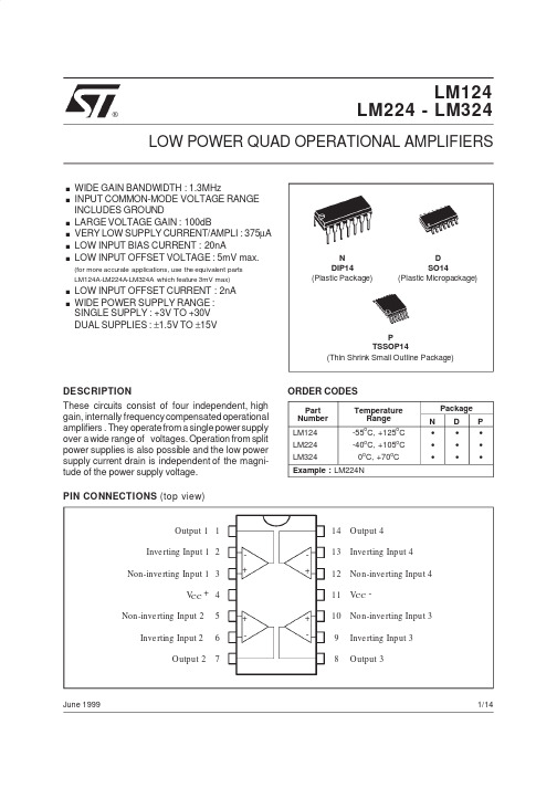
LOW INPUT OFFSET CURRENT : 2nA WIDE POWER SUPPLY RANGE : SINGLE SUPPLY : +3V TO +30V DUAL SUPPLIES : ±1.5V TO ±15V
P TSSOP14 (Thin Shrink Small Outline Package)
DESCRIPTION These circuits consist of four independent, high gain, internally frequency compensated operational amplifiers . They operate from a single power supply over a wide range of voltages. Operation from split power supplies is also possible and the low power supply current drain is independent of the magnitude of the power supply voltage. PIN CONNECTIONS (top view)
LM224中文资料_数据手册_参数
Parameter Supply Voltage
Input Voltage
Differential Input Voltage - (*)
Power Dissipation
N Suffix D Suffix
Output Short-circuit Duration - (note 1)
Supply Voltage Rejection (VCCT+am=b5=V+t2o53o0CV)
Ratio
(RS
≤
10kΩ)
Tmin. ≤ Tamb ≤ Tmax.
Supply Current, all Amp, no load
Tamb = +25oC
VCC = +5V
VCC = +30V
Tmin. ≤ Tamb ≤ Tmax.
(VCCTa=mb+5=V+,2R5LoC= 2kΩ)
Tmin. ≤ Tamb ≤ Tmax.
RL = 2kΩ RL = 10kΩ
Low Level Tamb =
Output +25oC
Voltage
(RL
=
10kΩ)
Tmin. ≤ Tamb ≤ Tmax.
Slew Rate VCC = 15V, VI = 0.5 to 3V, RL = 2kΩ, CL = 100pF, unity gain)
Input Offset Current Drift
Channel Separation (note 5) 1kHz ≤ f ≤ 20kHz
MHz
1.3 %
0.015
nV
40
lm224芯片工作原理

lm224芯片工作原理
LM224是一款运算放大器芯片,它是一种集成电路,用于放大电压信号。
LM224芯片工作原理涉及到运算放大器的基本原理和内部电路结构。
首先,让我们来了解一下运算放大器的基本原理。
运算放大器是一种差分放大器,它具有高输入阻抗、高增益、低输出阻抗等特点。
运算放大器内部通常由多级放大器级联构成,以实现高增益。
其基本工作原理是根据输入电压信号的差异来输出相应的放大电压信号。
LM224芯片内部的电路结构通常包括多级放大器、反馈网络、输入端和输出端等部分。
通过合理设计这些部分的结构,LM224芯片能够实现稳定的放大功能。
具体来说,LM224芯片通常包括四个运算放大器,每个运算放大器都具有非常高的输入阻抗和低的输出阻抗,以及高增益。
在实际应用中,LM224芯片通常用于信号放大、滤波、比较器等电路中。
通过合理设计外部电路连接方式和反馈网络,可以实现不同的功能,如比较、滤波、积分等。
LM224芯片还可以通过外部
电路实现负反馈和正反馈,从而实现不同的放大模式和功能。
总的来说,LM224芯片的工作原理涉及到运算放大器的基本原理和内部电路结构。
它通过合理设计内部电路和外部连接方式,实现了稳定的放大功能,广泛应用于各种电子电路中。
LM224LM324中文资料Word版
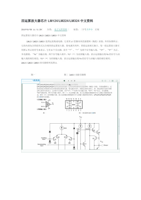
四运算放大器芯片LM124/LM224/LM324中文资料2010-01-30 11:41:29| 分类:电子元件资料 | 标签: |字号大中小订阅四运算放大器芯片LM124/LM224/LM324中文资料LM124/LM224/LM324是四运放集成电路,它采用14管脚双列直插塑料(陶瓷)封装,外形如图所示。
它的内部包含四组形式完全相同的运算放大器,除电源共用外,四组运放相互独立。
每一组运算放大器可用图1所示的符号来表示,它有5个引出脚,其中“+”、“-”为两个信号输入端,“V+”、“V-”为正、负电源端,“Vo”为输出端。
两个信号输入端中,Vi-(-)为反相输入端,表示运放输出端Vo的信号与该输入端的相位相反;Vi+(+)为同相输入端,表示运放输出端Vo的信号与该输入端的相位相同。
LM124/LM224/LM324的引脚排列见图2。
图一图二 lm324功能引脚图图3 LM324/LM124/LM224集成电路内部电路图 1/4主要参数:参数名称测试条件最小典型最大单位输入失调电压U0≈1.4V RS=0-2.07.0mV输入失调电流--5.050nA输入偏置电流--45250nA大信号电压增益U+=15V,RL=5kΩ88k100k--电源电流U+=30V,Uo=0,RL=∞ 1.53.0-mA共模抑制比Rs≤10kΩ6570-dB极限参数:LM124为陶瓷封装符号参数LM124LM224LM324单位VccSupply Voltage 电源电压±16 or 32VViInput Voltage 输入电压-0.3 to +32VVidDifferential Input Voltage -(*) 差分输入电压+32+32+32VPtotPower Dissipation功耗后缀N Suffix500500500mW后缀D Suffix-400400-Output Short-circuit Duration -(note 1)Infinite-IinInput Current (note 6) 输入电流505050mAToperOperating Free Air Temperature Range 工作温度-55 to +125-40 to +1050 to +70℃TstgStorage Temperature Range 储存温度范围-65 to +150-65 to +150-65 to +150℃由于LM124/LM224/LM324四运放电路具有电源电压范围宽,静态功耗小,可单电源使用,价格低廉等优点,因此被广泛应用在各种电路中。
LM324

PACKAGING INFORMATIONOrderableDevice Status (1)Package Type Package DrawingPins Package Qty Eco Plan (2)Lead/Ball Finish MSL Peak Temp (3)5962-7704301VCAACTIVE CDIP J 141TBD A42SNPB Level-NC-NC-NC 77043012A ACTIVE LCCC FK 201TBD POST-PLATE Level-NC-NC-NC7704301CA ACTIVE CDIP J 141TBD A42SNPB Level-NC-NC-NC 7704301DA ACTIVE CFP W 141TBD A42SNPB Level-NC-NC-NC 77043022A ACTIVE LCCC FK 201TBD POST-PLATE Level-NC-NC-NC7704302CA ACTIVE CDIP J 141TBD A42SNPB Level-NC-NC-NC JM38510/11005BCAACTIVE CDIP J 141TBD A42SNPB Level-NC-NC-NC LM124AFKB ACTIVE LCCC FK 201TBD POST-PLATE Level-NC-NC-NCLM124AJ ACTIVE CDIP J 141TBD A42SNPB Level-NC-NC-NC LM124AJB ACTIVE CDIP J 141TBD A42SNPB Level-NC-NC-NC LM124D ACTIVE SOIC D 1450TBD CU NIPDAU Level-3-245C-168HR LM124DR ACTIVE SOIC D 142500TBD CU NIPDAU Level-3-245C-168HR LM124FKB ACTIVE LCCC FK 201TBD POST-PLATE Level-NC-NC-NCLM124J ACTIVE CDIP J 141TBD A42SNPB Level-NC-NC-NC LM124JB ACTIVE CDIP J 141TBD A42SNPB Level-NC-NC-NC LM124N OBSOLETE PDIP N 14TBD Call TI Call TILM124W ACTIVE CFP W 141TBD A42SNPB Level-NC-NC-NC LM124WB ACTIVE CFP W 141TBD A42SNPB Level-NC-NC-NC LM224AD ACTIVE SOIC D 1450Green (RoHS &no Sb/Br)CU NIPDAU Level-1-260C-UNLIM LM224ADE4ACTIVE SOIC D 1450Green (RoHS &no Sb/Br)CU NIPDAU Level-1-260C-UNLIM LM224ADR ACTIVE SOIC D 142500Green (RoHS &no Sb/Br)CU NIPDAU Level-1-260C-UNLIM LM224ADRE4ACTIVE SOIC D 142500Green (RoHS &no Sb/Br)CU NIPDAU Level-1-260C-UNLIM LM224AN ACTIVE PDIP N 1425Pb-Free (RoHS)CU NIPDAU Level-NC-NC-NC LM224D ACTIVE SOIC D 1450Green (RoHS &no Sb/Br)CU NIPDAU Level-1-260C-UNLIM LM224DE4ACTIVE SOIC D 1450Green (RoHS &no Sb/Br)CU NIPDAU Level-1-260C-UNLIM LM224DR ACTIVE SOIC D 142500Green (RoHS &no Sb/Br)CU NIPDAU Level-1-260C-UNLIM LM224DRE4ACTIVE SOIC D 142500Green (RoHS &no Sb/Br)CU NIPDAU Level-1-260C-UNLIM LM224KAD ACTIVE SOIC D 1450Green (RoHS &no Sb/Br)CU NIPDAU Level-1-260C-UNLIM LM224KADE4ACTIVE SOIC D 1450Green (RoHS &no Sb/Br)CU NIPDAU Level-1-260C-UNLIM LM224KADR ACTIVE SOIC D 142500Green (RoHS &no Sb/Br)CU NIPDAU Level-1-260C-UNLIM LM224KADRE4ACTIVE SOIC D 142500Green (RoHS &no Sb/Br)CU NIPDAU Level-1-260C-UNLIM LM224KANACTIVEPDIPN1425Pb-Free (RoHS)CU NIPDAULevel-NC-NC-NCPACKAGE OPTION ADDENDUM9-Aug-2005Addendum-Page 1OrderableDeviceStatus (1)Package Type Package Drawing Pins Package Qty Eco Plan (2)Lead/Ball Finish MSL Peak Temp (3)LM224KANE4ACTIVE PDIP N 1425Pb-Free (RoHS)CU NIPDAU Level-NC-NC-NC LM224KDACTIVE SOIC D 1450Green (RoHS &no Sb/Br)CU NIPDAU Level-1-260C-UNLIM LM224KDE4ACTIVE SOIC D 1450Green (RoHS &no Sb/Br)CU NIPDAU Level-1-260C-UNLIM LM224KDRACTIVE SOIC D 142500Green (RoHS &no Sb/Br)CU NIPDAU Level-1-260C-UNLIM LM224KDRE4ACTIVE SOIC D 142500Green (RoHS &no Sb/Br)CU NIPDAU Level-1-260C-UNLIM LM224KNACTIVE PDIP N 1425Pb-Free (RoHS)CU NIPDAU Level-NC-NC-NC LM224KNE4ACTIVE PDIP N 1425Pb-Free (RoHS)CU NIPDAU Level-NC-NC-NC LM224NACTIVE PDIP N 1425Pb-Free (RoHS)CU NIPDAU Level-NC-NC-NC LM2902DACTIVE SOIC D 1450Green (RoHS &no Sb/Br)CU NIPDAU Level-1-260C-UNLIM LM2902DE4ACTIVE SOIC D 1450Green (RoHS &no Sb/Br)CU NIPDAU Level-1-260C-UNLIM LM2902DG4ACTIVE SOIC D 1450Green (RoHS &no Sb/Br)CU NIPDAU Level-1-260C-UNLIM LM2902DRACTIVE SOIC D 142500Green (RoHS &no Sb/Br)CU NIPDAU Level-1-260C-UNLIM LM2902DRE4ACTIVE SOIC D 142500Green (RoHS &no Sb/Br)CU NIPDAU Level-1-260C-UNLIM LM2902DRG4ACTIVE SOIC D 142500Green (RoHS &no Sb/Br)CU NIPDAU Level-1-260C-UNLIM LM2902KAVQDRACTIVE SOIC D 142500Pb-Free (RoHS)CU NIPDAU Level-2-250C-1YEAR/Level-1-235C-UNLIM LM2902KAVQPWRACTIVE TSSOP PW 142000TBD CU NIPDAU Level-1-250C-UNLIM LM2902KDACTIVE SOIC D 1450Green (RoHS &no Sb/Br)CU NIPDAU Level-1-260C-UNLIM LM2902KDBACTIVE SSOP DB 1480Green (RoHS &no Sb/Br)CU NIPDAU Level-1-260C-UNLIM LM2902KDBE4ACTIVE SSOP DB 1480Green (RoHS &no Sb/Br)CU NIPDAU Level-1-260C-UNLIM LM2902KDBRACTIVE SSOP DB 142000Green (RoHS &no Sb/Br)CU NIPDAU Level-1-260C-UNLIM LM2902KDBRE4ACTIVE SSOP DB 142000Green (RoHS &no Sb/Br)CU NIPDAU Level-1-260C-UNLIM LM2902KDE4ACTIVE SOIC D 1450Green (RoHS &no Sb/Br)CU NIPDAU Level-1-260C-UNLIM LM2902KDRACTIVE SOIC D 142500Green (RoHS &no Sb/Br)CU NIPDAU Level-1-260C-UNLIM LM2902KDRE4ACTIVE SOIC D 142500Green (RoHS &no Sb/Br)CU NIPDAU Level-1-260C-UNLIM LM2902KNACTIVE PDIP N 1425Pb-Free (RoHS)CU NIPDAU Level-NC-NC-NC LM2902KNE4ACTIVE PDIP N 1425Pb-Free(RoHS)CU NIPDAU Level-NC-NC-NC 9-Aug-2005OrderableDeviceStatus (1)Package Type Package Drawing Pins Package Qty Eco Plan (2)Lead/Ball Finish MSL Peak Temp (3)LM2902KNSRACTIVE SO NS 142000Green (RoHS &no Sb/Br)CU NIPDAU Level-1-260C-UNLIM LM2902KNSRE4ACTIVE SO NS 142000Green (RoHS &no Sb/Br)CU NIPDAU Level-1-260C-UNLIM LM2902KPWACTIVE TSSOP PW 1490Green (RoHS &no Sb/Br)CU NIPDAU Level-1-260C-UNLIM LM2902KPWE4ACTIVE TSSOP PW 1490Green (RoHS &no Sb/Br)CU NIPDAU Level-1-260C-UNLIM LM2902KPWRACTIVE TSSOP PW 142000Green (RoHS &no Sb/Br)CU NIPDAU Level-1-260C-UNLIM LM2902KPWRE4ACTIVE TSSOP PW 142000Green (RoHS &no Sb/Br)CU NIPDAU Level-1-260C-UNLIM LM2902KVQDRACTIVE SOIC D 142500Pb-Free (RoHS)CU NIPDAU Level-2-250C-1YEAR/Level-1-235C-UNLIM LM2902KVQPWRACTIVE TSSOP PW 142000TBD CU NIPDAU Level-1-250C-UNLIM LM2902NACTIVE PDIP N 1425Pb-Free (RoHS)CU NIPDAU Level-NC-NC-NC LM2902NE4ACTIVE PDIP N 1425Pb-Free (RoHS)CU NIPDAU Level-NC-NC-NC LM2902NSRACTIVE SO NS 142000Green (RoHS &no Sb/Br)CU NIPDAU Level-1-260C-UNLIM LM2902NSRG4ACTIVE SO NS 142000Green (RoHS &no Sb/Br)CU NIPDAU Level-1-260C-UNLIM LM2902PWACTIVE TSSOP PW 1490Green (RoHS &no Sb/Br)CU NIPDAU Level-1-260C-UNLIM LM2902PWE4ACTIVE TSSOP PW 1490Green (RoHS &no Sb/Br)CU NIPDAU Level-1-260C-UNLIM LM2902PWG4ACTIVE TSSOP PW 1490Green (RoHS &no Sb/Br)CU NIPDAU Level-1-260C-UNLIM LM2902PWLEOBSOLETE TSSOP PW 14TBD Call TI Call TI LM2902PWRACTIVE TSSOP PW 142000Green (RoHS &no Sb/Br)CU NIPDAU Level-1-260C-UNLIM LM2902PWRE4ACTIVE TSSOP PW 142000Green (RoHS &no Sb/Br)CU NIPDAU Level-1-260C-UNLIM LM2902PWRG4ACTIVE TSSOP PW 142000Green (RoHS &no Sb/Br)CU NIPDAU Level-1-260C-UNLIM LM2902QNOBSOLETE PDIP N 14TBD Call TI Call TI LM324ADACTIVE SOIC D 1450Green (RoHS &no Sb/Br)CU NIPDAU Level-1-260C-UNLIM LM324ADBLEOBSOLETE SSOP DB 14TBD Call TI Call TI LM324ADBRACTIVE SSOP DB 142000Green (RoHS &no Sb/Br)CU NIPDAU Level-1-260C-UNLIM LM324ADBRE4ACTIVE SSOP DB 142000Green (RoHS &no Sb/Br)CU NIPDAU Level-1-260C-UNLIM LM324ADE4ACTIVE SOIC D 1450Green (RoHS &no Sb/Br)CU NIPDAU Level-1-260C-UNLIM LM324ADRACTIVE SOIC D 142500Green (RoHS &no Sb/Br)CU NIPDAU Level-1-260C-UNLIM LM324ADRE4ACTIVE SOIC D 142500Green (RoHS &no Sb/Br)CU NIPDAU Level-1-260C-UNLIM LM324AN ACTIVE PDIP N 1425Pb-FreeCU NIPDAU Level-NC-NC-NC 9-Aug-2005OrderableDevice Status (1)PackageType Package Drawing Pins Package Qty Eco Plan (2)Lead/Ball Finish MSL Peak Temp (3)(RoHS)LM324ANE4ACTIVE PDIPN 1425Pb-Free (RoHS)CU NIPDAU Level-NC-NC-NC LM324ANSR ACTIVE SONS 142000Green (RoHS &no Sb/Br)CU NIPDAU Level-1-260C-UNLIM LM324ANSRE4ACTIVE SONS 142000Green (RoHS &no Sb/Br)CU NIPDAU Level-1-260C-UNLIM LM324APW ACTIVE TSSOPPW 1490Green (RoHS &no Sb/Br)CU NIPDAU Level-1-260C-UNLIM LM324APWE4ACTIVE TSSOPPW 1490Green (RoHS &no Sb/Br)CU NIPDAU Level-1-260C-UNLIM LM324APWG4ACTIVE TSSOPPW 1490Green (RoHS &no Sb/Br)CU NIPDAU Level-1-260C-UNLIM LM324APWLE OBSOLETE TSSOPPW 14TBD Call TI Call TI LM324APWR ACTIVE TSSOPPW 142000Green (RoHS &no Sb/Br)CU NIPDAU Level-1-260C-UNLIM LM324APWRE4ACTIVE TSSOPPW 142000Green (RoHS &no Sb/Br)CU NIPDAU Level-1-260C-UNLIM LM324APWRG4ACTIVE TSSOPPW 142000Green (RoHS &no Sb/Br)CU NIPDAU Level-1-260C-UNLIM LM324D ACTIVE SOICD 1450Green (RoHS &no Sb/Br)CU NIPDAU Level-1-260C-UNLIM LM324DE4ACTIVE SOICD 1450Green (RoHS &no Sb/Br)CU NIPDAU Level-1-260C-UNLIM LM324DG4ACTIVE SOICD 1450Green (RoHS &no Sb/Br)CU NIPDAU Level-1-260C-UNLIM LM324DR ACTIVE SOICD 142500Green (RoHS &no Sb/Br)CU NIPDAU Level-1-260C-UNLIM LM324DRE4ACTIVE SOICD 142500Green (RoHS &no Sb/Br)CU NIPDAU Level-1-260C-UNLIM LM324DRG4ACTIVE SOICD 142500Green (RoHS &no Sb/Br)CU NIPDAU Level-1-260C-UNLIM LM324KAD ACTIVE SOICD 1450Green (RoHS &no Sb/Br)CU NIPDAU Level-1-260C-UNLIM LM324KADG4ACTIVE SOICD 1450Green (RoHS &no Sb/Br)CU NIPDAU Level-1-260C-UNLIM LM324KADR ACTIVE SOICD 142500Green (RoHS &no Sb/Br)CU NIPDAU Level-1-260C-UNLIM LM324KADRG4ACTIVE SOICD 142500Green (RoHS &no Sb/Br)CU NIPDAU Level-1-260C-UNLIM LM324KAN ACTIVE PDIPN 1425Pb-Free (RoHS)CU NIPDAU Level-NC-NC-NC LM324KANE4ACTIVE PDIPN 1425Pb-Free (RoHS)CU NIPDAU Level-NC-NC-NC LM324KANS PREVIEW SONS 1450Green (RoHS &no Sb/Br)CU NIPDAU Level-1-260C-UNLIM LM324KANSR ACTIVE SONS 142000Green (RoHS &no Sb/Br)CU NIPDAU Level-1-260C-UNLIM LM324KANSRE4ACTIVE SONS 142000Green (RoHS &no Sb/Br)CU NIPDAU Level-1-260C-UNLIM LM324KAPW ACTIVE TSSOP PW 1490Green (RoHS &CU NIPDAU Level-1-260C-UNLIM 9-Aug-2005OrderableDevice Status (1)PackageType Package Drawing Pins Package Qty Eco Plan (2)Lead/Ball Finish MSL Peak Temp (3)no Sb/Br)LM324KAPWG4ACTIVE TSSOPPW 1490Green (RoHS &no Sb/Br)CU NIPDAU Level-1-260C-UNLIM LM324KAPWR ACTIVE TSSOPPW 142000Green (RoHS &no Sb/Br)CU NIPDAU Level-1-260C-UNLIM LM324KAPWRG4ACTIVE TSSOPPW 142000Green (RoHS &no Sb/Br)CU NIPDAU Level-1-260C-UNLIM LM324KD ACTIVE SOICD 1450Green (RoHS &no Sb/Br)CU NIPDAU Level-1-260C-UNLIM LM324KDE4ACTIVE SOICD 1450Green (RoHS &no Sb/Br)CU NIPDAU Level-1-260C-UNLIM LM324KDR ACTIVE SOICD 142500Green (RoHS &no Sb/Br)CU NIPDAU Level-1-260C-UNLIM LM324KDRE4ACTIVE SOICD 142500Green (RoHS &no Sb/Br)CU NIPDAU Level-1-260C-UNLIM LM324KN ACTIVE PDIPN 1425Pb-Free (RoHS)CU NIPDAU Level-NC-NC-NC LM324KNS PREVIEW SONS 1450Green (RoHS &no Sb/Br)CU NIPDAU Level-1-260C-UNLIM LM324KNSR ACTIVE SONS 142000Green (RoHS &no Sb/Br)CU NIPDAU Level-1-260C-UNLIM LM324KNSRE4ACTIVE SONS 142000Green (RoHS &no Sb/Br)CU NIPDAU Level-1-260C-UNLIM LM324KPW ACTIVE TSSOPPW 1490Green (RoHS &no Sb/Br)CU NIPDAU Level-1-260C-UNLIM LM324KPWE4ACTIVE TSSOPPW 1490Green (RoHS &no Sb/Br)CU NIPDAU Level-1-260C-UNLIM LM324KPWR ACTIVE TSSOPPW 142000Green (RoHS &no Sb/Br)CU NIPDAU Level-1-260C-UNLIM LM324KPWRE4ACTIVE TSSOPPW 142000Green (RoHS &no Sb/Br)CU NIPDAU Level-1-260C-UNLIM LM324N ACTIVE PDIPN 1425Pb-Free (RoHS)CU NIPDAU Level-NC-NC-NC LM324NE4ACTIVE PDIPN 1425Pb-Free (RoHS)CU NIPDAU Level-NC-NC-NC LM324NSR ACTIVE SONS 142000Green (RoHS &no Sb/Br)CU NIPDAU Level-1-260C-UNLIM LM324NSRE4ACTIVE SONS 142000Green (RoHS &no Sb/Br)CU NIPDAU Level-1-260C-UNLIM LM324NSRG4ACTIVE SONS 142000Green (RoHS &no Sb/Br)CU NIPDAU Level-1-260C-UNLIM LM324PW ACTIVE TSSOPPW 1490Green (RoHS &no Sb/Br)CU NIPDAU Level-1-260C-UNLIM LM324PWE4ACTIVE TSSOPPW 1490Green (RoHS &no Sb/Br)CU NIPDAU Level-1-260C-UNLIM LM324PWG4ACTIVE TSSOPPW 1490Green (RoHS &no Sb/Br)CU NIPDAU Level-1-260C-UNLIM LM324PWLE OBSOLETE TSSOPPW 14TBD Call TI Call TI LM324PWR ACTIVE TSSOPPW 142000Green (RoHS &no Sb/Br)CU NIPDAU Level-1-260C-UNLIM LM324PWRE4ACTIVE TSSOP PW 142000Green (RoHS &CU NIPDAU Level-1-260C-UNLIM 9-Aug-2005Orderable Device Status (1)PackageTypePackage Drawing Pins Package Qty Eco Plan (2)Lead/Ball Finish MSL Peak Temp (3)no Sb/Br)LM324PWRG4ACTIVE TSSOPPW 142000Green (RoHS &no Sb/Br)CU NIPDAU Level-1-260C-UNLIM LM324YOBSOLETE XCEPT Y 0TBD Call TI Call TI (1)The marketing status values are defined as follows:ACTIVE:Product device recommended for new designs.LIFEBUY:TI has announced that the device will be discontinued,and a lifetime-buy period is in effect.NRND:Not recommended for new designs.Device is in production to support existing customers,but TI does not recommend using this part in a new design.PREVIEW:Device has been announced but is not in production.Samples may or may not be available.OBSOLETE:TI has discontinued the production of the device.(2)Eco Plan -The planned eco-friendly classification:Pb-Free (RoHS)or Green (RoHS &no Sb/Br)-please check /productcontent for the latest availability information and additional product content details.TBD:The Pb-Free/Green conversion plan has not been defined.Pb-Free (RoHS):TI's terms "Lead-Free"or "Pb-Free"mean semiconductor products that are compatible with the current RoHS requirements for all 6substances,including the requirement that lead not exceed 0.1%by weight in homogeneous materials.Where designed to be soldered at high temperatures,TI Pb-Free products are suitable for use in specified lead-free processes.Green (RoHS &no Sb/Br):TI defines "Green"to mean Pb-Free (RoHS compatible),and free of Bromine (Br)and Antimony (Sb)based flame retardants (Br or Sb do not exceed 0.1%by weight in homogeneous material)(3)MSL,Peak Temp.--The Moisture Sensitivity Level rating according to the JEDEC industry standard classifications,and peak solder temperature.Important Information and Disclaimer:The information provided on this page represents TI's knowledge and belief as of the date that it is provided.TI bases its knowledge and belief on information provided by third parties,and makes no representation or warranty as to the accuracy of such information.Efforts are underway to better integrate information from third parties.TI has taken and continues to take reasonable stepsto provide representative and accurate information but may not have conducted destructive testing or chemical analysis on incoming materials and chemicals.TI and TI suppliers consider certain information to be proprietary,and thus CAS numbers and other limited information may not be available for release.In no event shall TI's liability arising out of such information exceed the total purchase price of the TI part(s)at issue in this document sold by TI to Customer on an annual basis. 9-Aug-2005IMPORTANT NOTICETexas Instruments Incorporated and its subsidiaries (TI) reserve the right to make corrections, modifications, enhancements, improvements, and other changes to its products and services at any time and to discontinue any product or service without notice. Customers should obtain the latest relevant information before placing orders and should verify that such information is current and complete. All products are sold subject to TI’s terms and conditions of sale supplied at the time of order acknowledgment.TI warrants performance of its hardware products to the specifications applicable at the time of sale in accordance with TI’s standard warranty. T esting and other quality control techniques are used to the extent TI deems necessary to support this warranty. Except where mandated by government requirements, testing of all parameters of each product is not necessarily performed.TI assumes no liability for applications assistance or customer product design. Customers are responsible for their products and applications using TI components. T o minimize the risks associated with customer products and applications, customers should provide adequate design and operating safeguards.TI does not warrant or represent that any license, either express or implied, is granted under any TI patent right, copyright, mask work right, or other TI intellectual property right relating to any combination, machine, or process in which TI products or services are used. Information published by TI regarding third-party products or services does not constitute a license from TI to use such products or services or a warranty or endorsement thereof. Use of such information may require a license from a third party under the patents or other intellectual property of the third party, or a license from TI under the patents or other intellectual property of TI.Reproduction of information in TI data books or data sheets is permissible only if reproduction is without alteration and is accompanied by all associated warranties, conditions, limitations, and notices. Reproduction of this information with alteration is an unfair and deceptive business practice. TI is not responsible or liable for such altered documentation.Resale of TI products or services with statements different from or beyond the parameters stated by TI for that product or service voids all express and any implied warranties for the associated TI product or service and is an unfair and deceptive business practice. TI is not responsible or liable for any such statements. Following are URLs where you can obtain information on other Texas Instruments products and application solutions:Products ApplicationsAmplifiers Audio /audioData Converters Automotive /automotiveDSP Broadband /broadbandInterface Digital Control /digitalcontrolLogic Military /militaryPower Mgmt Optical Networking /opticalnetwork Microcontrollers Security /securityTelephony /telephonyVideo & Imaging /videoWireless /wirelessMailing Address:Texas InstrumentsPost Office Box 655303 Dallas, Texas 75265Copyright 2005, Texas Instruments Incorporated。
LM124四运算放大器芯片的中文应用资料

四运算放大器芯片的中文应用资料LM124/LM224/LM324是四运放集成电路,它采用14管脚双列直插塑料(陶瓷)封装,外形如图所示。
它的内部包含四组形式完全相同的运算放大器,除电源共用外,四组运放相互独立。
每一组运算放大器可用图1所示的符号来表示,它有5个引出脚,其中“+”、“-”为两个信号输入端,“V+”、“V-”为正、负电源端,“Vo”为输出端。
两个信号输入端中,Vi-(-)为反相输入端,表示运放输出端Vo的信号与该输入端的相位相反;Vi+(+)为同相输入端,表示运放输出端Vo的信号与该输入端的相位相同。
LM124/LM224/LM324的引脚排列见图2。
图一图二lm324功能引脚图图3 LM324/LM124/LM224集成电路内部电路图1/4主要参数:参数名称测试条件最小典型最大单位输入失调电压U0≈1.4V RS=0 - 2.07.0mV输入失调电流 - - 5.050nA输入偏置电流 - -45250nA大信号电压增益U+=15V,R L=5kΩ 88k100k --电源电流U+=30V,U o=0,R L=∞ 1.5 3.0 -mA 共模抑制比R s≤10kΩ6570 -dB极限参数:LM124为陶瓷封装符号参数LM124 LM224 LM324 单位Vcc Supply Voltage 电源电压±16 or 32 V Vi Input Voltage 输入电压-0.3 to +32 VVid Differential InputVoltage -(*) 差分输入电压+32 +32 +32 VPtot PowerDissipation功耗后缀NSuffix500 500 500mW后缀DSuffix-400 400-Output Short-circuitDuration -(note 1)Infinite-Iin Input Current (note 6)输入电流50 50 50 mAToper Operating Free AirTemperature Range 工作温度-55 to+125-40 to+1050 to +70 ℃Tstg Storage TemperatureRange 储存温度范围-65 to+150-65 to+150-65 to+150℃由于LM124/LM224/LM324四运放电路具有电源电压范围宽,静态功耗小,可单电源使用,价格低廉等优点,因此被广泛应用在各种电路中。
LM324系列 LM224 LM324规格书推荐

LM324, LM324A, LM324E, LM224, LM2902, LM2902E, LM2902V, NCV2902Single Supply Quad Operational AmplifiersThe LM324 series are low−cost, quad operational amplifiers with true differential inputs. They have several distinct advantages over standard operational amplifier types in single supply applications. Thequad amplifier can operate at supply voltages as low as 3.0 V or as high as 32 V with quiescent currents about one−fifth of those associated with the MC1741 (on a per amplifier basis). The common mode input range includes the negative supply, thereby eliminating the necessity for external biasing components in many applications. The output voltage range also includes the negative power supply voltage. Features•Short Circuited Protected Outputs•True Differential Input Stage•Single Supply Operation: 3.0 V to 32 V•Low Input Bias Currents: 100 nA Maximum (LM324A)•Four Amplifiers Per Package•Internally Compensated•Common Mode Range Extends to Negative Supply •Industry Standard Pinouts•ESD Clamps on the Inputs Increase Ruggedness without Affecting Device Operation•NCV Prefix for Automotive and Other Applications Requiring Unique Site and Control Change Requirements; AEC−Q100 Qualified and PPAP Capable•These Devices are Pb−Free, Halogen Free/BFR Free and are RoHS CompliantPDIP−14N SUFFIXCASE 646114SOIC−14D SUFFIXCASE 751A1PIN CONNECTIONSOut 4Inputs 4V EE, GNDInputs 3Out 3V(Top View)See general marking information in the device marking section on page 11 of this data sheet.DEVICE MARKING INFORMATIONSee detailed ordering and shipping information in the package dimensions section on page 10 of this data sheet.ORDERING INFORMATIONTSSOP−14DTB SUFFIXCASE 948GMAXIMUM RATINGS (T A = +25°C, unless otherwise noted.)Rating Symbol Value Unit Power Supply Voltages Vdc Single Supply V CC32Split Supplies V CC, V EE±16Input Differential Voltage Range (Note 1)V IDR±32Vdc Input Common Mode Voltage Range V ICR−0.3 to 32Vdc Output Short Circuit Duration t SC ContinuousJunction Temperature T J150°CThermal Resistance, Junction−to−Air (Note 2)Case 646Case 751ACase 948G R q JA118156190°C/WStorage Temperature Range T stg−65 to +150°C Operating Ambient Temperature Range T A°CLM224−25 to +85LM324, LM324A, LM324E0 to +70LM2902, LM2902E−40 to +105LM2902V, NCV2902 (Note 3)−40 to +125Stresses exceeding those listed in the Maximum Ratings table may damage the device. If any of these limits are exceeded, device functionality should not be assumed, damage may occur and reliability may be affected.1.Split Power Supplies.2.All R q JA measurements made on evaluation board with 1 oz. copper traces of minimum pad size. All device outputs were active.3.NCV2902 is qualified for automitive use.ESD RATINGSRating HBM MM Unit ESD Protection at any Pin (Human Body Model − HBM, Machine Model − MM)NCV2902 (Note 3)LM324E, LM2902ELM324DG/DR2G, LM2902DG/DR2G All Other Devices 200020002002000200200100200VVVVCharacteristics Symbol Min Typ Max Min Typ Max Min Typ Max Min Typ Max Min Typ Max UnitInput Offset Voltage V IO mV V CC = 5.0 V to 30 VV ICR = 0 V toV CC −1.7 V,V O = 1.4 V, R S = 0 WT A = 25°C− 2.0 5.0− 2.0 3.0− 2.07.0− 2.07.0− 2.07.0T A = T high (Note 4)−−7.0−− 5.0−−9.0−−10−−13T A = T low (Note 4)−−7.0−− 5.0−−9.0−−10−−10D V IO/D T−7.0−−7.030−7.0−−7.0−−7.0−m V/°C Average TemperatureCoefficient of InputOffset VoltageT A = T high to T low(Notes 4 and 6)Input Offset Current I IO− 3.030− 5.030− 5.050− 5.050− 5.050nA−−100−−75−−150−−200−−200T A = T high to T low(Note 4)D I IO/D T−10−−10300−10−−10−−10−pA/°C Average T emperatureCoefficient of InputOffset CurrentT A = T high to T low(Notes 4 and 6)Input Bias Current I IB−−90−150−−45−100−−90−250−−90−250−−90−250nA−−−300−−−200−−−500−−−500−−−500T A = T high to T low(Note 4)Input Common ModeV ICR V Voltage Range(Note 5)V CC = 30 VT A = +25°C0−28.30−28.30−28.30−28.30−28.30−280−280−280−280−28T A = T high to T low(Note 4)Differential InputV IDR−−V CC−−V CC−−V CC−−V CC−−V CC V Voltage RangeA VOL V/mV Large Signal OpenLoop Voltage Gain50100−25100−25100−25100−25100−R L = 2.0 k W,V CC = 15 V,for Large V O Swing25−−15−−15−−15−−15−−T A = T high to T low(Note 4)CS−−120−−−120−−−120−−−120−−−120−dB Channel Separation10 kHz ≤ f ≤ 20 kHz,Input ReferencedCommon ModeCMR7085−6570−6570−5070−5070−dB Rejection,R S≤ 10 k WPSR65100−65100−65100−50100−50100−dB Power SupplyRejection4.LM224: T low = −25°C, T high = +85°CLM324/LM324A/LM324E: T low = 0°C, T high = +70°CLM2902/LM2902E: T low = −40°C, T high = +105°CLM2902V & NCV2902: T low = −40°C, T high = +125°CNCV2902 is qualified for automotive use.5.The input common mode voltage or either input signal voltage should not be allowed to go negative by more than 0.3 V. The upper end ofthe common mode voltage range is V CC −1.7 V, but either or both inputs can go to +32 V without damage, independent of the magnitude of V CC.6.Guaranteed by design.Characteristics Symbol Min Typ Max Min Typ Max Min Typ Max Min Typ Max Min Typ Max Unit Output Voltage−V OH V High Limit3.3 3.5− 3.3 3.5− 3.3 3.5− 3.3 3.5− 3.3 3.5−V CC = 5.0 V, R L =2.0 k W, T A = 25°C26−−26−−26−−26−−26−−V CC = 30 VR L = 2.0 k W(T A = T high to T low)(Note 7)2728−2728−2728−2728−2728−V CC = 30 VR L = 10 k W(T A = T high to T low)(Note 7)V OL− 5.020− 5.020− 5.020− 5.0100− 5.0100mV Output Voltage −Low Limit,V CC = 5.0 V,R L = 10 k W,T A = T high to T low(Note 7)I O+mA Output Source Current(V ID = +1.0 V,V CC = 15 V)T A = 25°C2040−2040−2040−2040−2040−1020−1020−1020−1020−1020−T A = T high to T low(Note 7)Output Sink Current I O−mA1020−1020−1020−1020−1020−(V ID = −1.0 V,V CC = 15 V)T A = 25°C5.08.0− 5.08.0− 5.08.0− 5.08.0− 5.08.0−T A = T high to T low(Note 7)1250−1250−1250−−−−−−−m A (V ID = −1.0 V,V O = 200 mV,T A = 25°C)Output Short CircuitI SC−4060−4060−4060−4060−4060mAto Ground(Note 8)I CC mA Power Supply Current(T A = T high to T low)(Note 7)−− 3.0− 1.4 3.0−− 3.0−− 3.0−− 3.0V CC = 30 VV O = 0 V, R L = ∞−− 1.2−0.7 1.2−− 1.2−− 1.2−− 1.2V CC = 5.0 V,V O = 0 V, R L = ∞7.LM224: T low = −25°C, T high = +85°CLM324/LM324A/LM324E: T low = 0°C, T high = +70°CLM2902/LM2902E: T low = −40°C, T high = +105°CLM2902V & NCV2902: T low = −40°C, T high = +125°CNCV2902 is qualified for automotive use.8.The input common mode voltage or either input signal voltage should not be allowed to go negative by more than 0.3 V. The upper end ofthe common mode voltage range is V CC −1.7 V, but either or both inputs can go to +32 V without damage, independent of the magnitude of V CC.Product parametric performance is indicated in the Electrical Characteristics for the listed test conditions, unless otherwise noted. Product performance may not be indicated by the Electrical Characteristics if operated under different conditions.Figure 1. Representative Circuit Diagram(One−Fourth of Circuit Shown)Bias Circuitry Common to Four V CCV EE /GND+CIRCUIT DESCRIPTION The LM324 series is made using four internally compensated, two−stage operational amplifiers. The firststage of each consists of differential input devices Q20 andQ18 with input buffer transistors Q21 and Q17 and thedifferential to single ended converter Q3 and Q4. The firststage performs not only the first stage gain function but alsoperforms the level shifting and transconductance reductionfunctions. By reducing the transconductance, a smaller compensation capacitor (only 5.0 pF) can be employed, thussaving chip area. The transconductance reduction is accomplished by splitting the collectors of Q20 and Q18.Another feature of this input stage is that the input common mode range can include the negative supply or ground, in single supply operation, without saturating either the input devices or the differential to single−ended converter. The second stage consists of a standard current source load amplifier stage.Figure 2. Large Signal Voltage Follower Response1.V/DIVEach amplifier is biased from an internal−voltage regulator which has a low temperature coefficient thus giving each amplifier good temperature characteristics aswell as excellent power supply rejection.Split Supplies3.0 V to VCC(max)EE(max)Figure 3.706050403020101.010********LOAD CAPACITANCE (pF)Figure 4. Gain and Phase Margin100070605040302010GAINMARGIN(dB)PHASE MARGIN (°)V O R , O U T P U T V O L T A G E R A N G E (V )p p V O , O U T P U T V O L T A G E (m V )f, FREQUENCY (kHz)t, TIME (m s)2.42.11.81.51.20.90.60.30V CC , POWER SUPPLY VOLTAGE (V)V CC , POWER SUPPLY VOLTAGE (V)9080700 2.0 4.06.08.0101214161820I , P O W E R S U P P L Y C U R R E N T (m A )C C I ,I N P U T B I A S C U R R E N T (n A )I B V , I N P U T V O L T A G E (V )I12020± V CC /V EE, POWER SUPPLY VOLTAGES (V)±Figure 5. Input Voltage Range Figure 6. Open Loop Frequency120100806040200-201.0101001.0 k10 k100 k1.0 Mf, FREQUENCY (Hz)A , L A R G E -S I G N A L V O L O P E N L O O P V O L T A G E G A I N (dB )Figure 7. Large−Signal Frequency ResponseFigure 8. Small−Signal Voltage FollowerPulse Response (Noninverting)Figure 9. Power Supply Current versusPower Supply Voltage Figure 10. Input Bias Current versusPower Supply Voltage21R1T BP R1 + R2R1R1 + R2e oe 1e 2e o = C (1 + a + b) (e 2 - e 1)V refV inV V V V inL =R1(V OL - V ref ) + V refV inH =(V OH - V ref ) + V refH =R1 + R2(V OH - V OL )R1reff o =2 p RC R1 = QRR2 =R3 = T N R2C1 = 10C 1Notch OutputV ref =V CCrefWhere: T BP = Center Frequency Gain T N = Passband Notch GainR = 160 k W C = 0.001 m F R1= 1.6 M W R2= 1.6 M W R3= 1.6 M W o = 1.0 kHz Q = 10T BP = 1T N = 1V OV refV ref = V 2V O 2p RC1f o = 1.0 kHzR = 16 k W C = 0.01 m FV O R1R21 =Figure 11. Voltage Reference Figure 12. Wien Bridge OscillatorFigure 13. High Impedance Differential Amplifier Figure 14. Comparator with HysteresisFigure 15. Bi−Quad Filter1For less than 10% error from operational amplifier,If source impedance varies, filter may be preceded with voltage follower buffer to stabilize filter parameters.where f o and BW are expressed in Hz.Q o f o BW< 0.1Given: f o = center frequencyA(f o ) = gain at center frequency Choose value f o , C Then:R3 =Q p f o C R3R1 = 2 A(f o )R1 R34Q 2 R1 - R3R2 =V ref V reff =R1 + R C 4 CR f R1R3 =R2 R1R2 + R1VR fif Figure 16. Function Generator Figure 17. Multiple Feedback Bandpass FilterV OORDERING INFORMATIONDevice Operating Temperature Range Package Shipping†LM224DG−25°C to +85°C SOIC−14 (Pb−Free)55 Units/RailLM224DR2G SOIC−14 (Pb−Free)2500/T ape & Reel LM224DTBG TSSOP−14 (Pb−Free)96 Units/Tube LM224DTBR2G TSSOP−14 (Pb−Free)2500/T ape & Reel LM224NG PDIP−14 (Pb−Free)25 Units/RailLM324DG0°C to +70°C SOIC−14 (Pb−Free)55 Units/RailLM324DR2G SOIC−14 (Pb−Free)2500/T ape & Reel LM324EDR2G SOIC−14 (Pb−Free)2500/T ape & Reel LM324DTBG TSSOP−14 (Pb−Free)96 Units/Tube LM324DTBR2G TSSOP−14 (Pb−Free)2500/T ape & Reel LM324NG PDIP−14 (Pb−Free)25 Units/Rail LM324ADG SOIC−14 (Pb−Free)55 Units/Rail LM324ADR2G SOIC−14 (Pb−Free)2500/T ape & Reel LM324ADTBG TSSOP−14 (Pb−Free)96 Units/Tube LM324ADTBR2G TSSOP−14 (Pb−Free)2500/T ape & Reel LM324ANG PDIP−14 (Pb−Free)25 Units/RailLM2902DG−40°C to +105°C SOIC−14 (Pb−Free)55 Units/RailLM2902DR2G SOIC−14 (Pb−Free)2500/T ape & Reel LM2902EDR2G SOIC−14 (Pb−Free)2500/T ape & Reel LM2902DTBG TSSOP−14 (Pb−Free)96 Units/Tube LM2902DTBR2G TSSOP−14 (Pb−Free)2500/T ape & Reel LM2902NG PDIP−14 (Pb−Free)25 Units/RailLM2902VDG−40°C to +125°C SOIC−14 (Pb−Free)55 Units/RailLM2902VDR2G SOIC−14 (Pb−Free)2500/T ape & ReelLM2902VDTBG TSSOP−14 (Pb−Free)96 Units/TubeLM2902VDTBR2G TSSOP−14 (Pb−Free)2500/T ape & ReelLM2902VNG PDIP−14 (Pb−Free)25 Units/RailNCV2902DR2G*SOIC−14 (Pb−Free)2500/T ape & ReelNCV2902DTBR2G*TSSOP−14 (Pb−Free)†For information on tape and reel specifications, including part orientation and tape sizes, please refer to our Tape and Reel Packaging Specifications Brochure, BRD8011/D.*NCV Prefix for Automotive and Other Applications Requiring Unique Site and Control Change Requirements; AEC−Q100 Qualified and PPAP Capable.MARKING DIAGRAMSx = 2 or 3A = Assembly Location WL, L = Wafer Lot YY , Y = YearWW, W = Work Week G or G = Pb−Free PackagePDIP−14N SUFFIX CASE 646SOIC−14D SUFFIX CASE 751A114LM324AN AWLYYWWG 114LMx24N AWLYYWWG114LM2902N AWLYYWWG114LM2902VN AWLYYWWG*This marking diagram also applies to NCV2902.TSSOP−14DTB SUFFIX CASE 948G114x24ALYW G G 114114114*324A ALYW G G2902ALYW G G2902V ALYW G G(Note: Microdot may be in either location)SOIC−14CASE 751A−03ISSUE KNOTES:1.DIMENSIONING AND TOLERANCING PERASME Y14.5M, 1994.2.CONTROLLING DIMENSION: MILLIMETERS.3.DIMENSION b DOES NOT INCLUDE DAMBARPROTRUSION. ALLOWABLE PROTRUSIONSHALL BE 0.13 TOTAL IN EXCESS OF ATMAXIMUM MATERIAL CONDITION.4.DIMENSIONS D AND E DO NOT INCLUDEMOLD PROTRUSIONS.5.MAXIMUM MOLD PROTRUSION 0.15 PERSIDE.DETAIL ADIM MIN MAX MIN MAXINCHESMILLIMETERSD8.558.750.3370.344E 3.80 4.000.1500.157A 1.35 1.750.0540.068b0.350.490.0140.019L0.40 1.250.0160.049e 1.27 BSC0.050 BSCA30.190.250.0080.010A10.100.250.0040.010M0 7 0 7H 5.80 6.200.2280.244h0.250.500.0100.019____14X0.581.27PITCH*For additional information on our Pb−Free strategy and solderingdetails, please download the ON Semiconductor Soldering andMounting Techniques Reference Manual, SOLDERRM/D.TSSOP−14CASE 948G ISSUE BDIM MIN MAX MIN MAX INCHES MILLIMETERS A 4.90 5.100.1930.200B 4.30 4.500.1690.177C −−− 1.20−−−0.047D 0.050.150.0020.006F 0.500.750.0200.030G 0.65 BSC 0.026 BSC H 0.500.600.0200.024J 0.090.200.0040.008J10.090.160.0040.006K 0.190.300.0070.012K10.190.250.0070.010L 6.40 BSC 0.252 BSC M0 8 0 8 NOTES:1.DIMENSIONING AND TOLERANCING PER ANSI Y14.5M, 1982.2.CONTROLLING DIMENSION: MILLIMETER.3.DIMENSION A DOES NOT INCLUDE MOLD FLASH, PROTRUSIONS OR GATE BURRS.MOLD FLASH OR GATE BURRS SHALL NOT EXCEED 0.15 (0.006) PER SIDE.4.DIMENSION B DOES NOT INCLUDE INTERLEAD FLASH OR PROTRUSION.INTERLEAD FLASH OR PROTRUSION SHALL NOT EXCEED 0.25 (0.010) PER SIDE.5.DIMENSION K DOES NOT INCLUDE DAMBAR PROTRUSION. ALLOWABLE DAMBARPROTRUSION SHALL BE 0.08 (0.003) TOTAL IN EXCESS OF THE K DIMENSION AT MAXIMUM MATERIAL CONDITION.6.TERMINAL NUMBERS ARE SHOWN FOR REFERENCE ONLY .7.DIMENSION A AND B ARE TO BEDETERMINED AT DATUM PLANE −W−.____14X REF K14X0.360.65PITCHSOLDERING FOOTPRINTPDIP−14CASE 646−06ISSUE SWITH LEADS CONSTRAINEDDIM MIN MAX INCHES A −−−−0.210A10.015−−−−b 0.0140.022C 0.0080.014D 0.7350.775D10.005−−−−e 0.100 BSC E 0.3000.325M−−−−10−−− 5.330.38−−−0.350.560.200.3618.6719.690.13−−−2.54 BSC 7.628.26−−−10MIN MAX MILLIMETERSNOTES:1.DIMENSIONING AND TOLERANCING PER ASME Y14.5M, 1994.2.CONTROLLING DIMENSION: INCHES.3.DIMENSIONS A, A1 AND L ARE MEASURED WITH THE PACK-AGE SEATED IN JEDEC SEATING PLANE GAUGE GS−3.4.DIMENSIONS D, D1 AND E1 DO NOT INCLUDE MOLD FLASH OR PROTRUSIONS. MOLD FLASH OR PROTRUSIONS ARE NOT TO EXCEED 0.10 INCH.5.DIMENSION E IS MEASURED AT A POINT 0.015 BELOW DATUM PLANE H WITH THE LEADS CONSTRAINED PERPENDICULAR TO DATUM C.6.DIMENSION eB IS MEASURED AT THE LEAD TIPS WITH THE LEADS UNCONSTRAINED.7.DATUM PLANE H IS COINCIDENT WITH THE BOTTOM OF THE LEADS, WHERE THE LEADS EXIT THE BODY .8.PACKAGE CONTOUR IS OPTIONAL (ROUNDED OR SQUARE CORNERS).E10.2400.280 6.107.11b2eB −−−−0.430−−−10.920.060 TYP 1.52 TYP A20.1150.195 2.92 4.95L 0.1150.150 2.92 3.81°°ON Semiconductor and are trademarks of Semiconductor Components Industries, LLC dba ON Semiconductor or its subsidiaries in the United States and/or other countries.ON Semiconductor owns the rights to a number of patents, trademarks, copyrights, trade secrets, and other intellectual property. A listing of ON Semiconductor’s product/patent PUBLICATION ORDERING INFORMATION。
直流电机无级调整电路板的方法及原理图
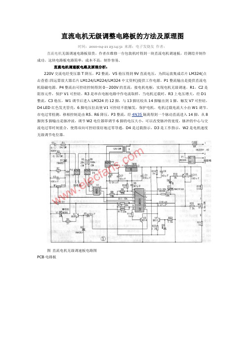
直流电机无级调整电路板的方法及原理图时间:2010-04-21 23:14:51 来源:电子发烧友作者:直流电机无级调速电路板很贵,作者在维修一台包装机时得到一块直流电机调速板,经测绘并制作成功。
这块电路板电路简单,成本不高,制作容易.直流电机调速板电路及原理分析:220V交流电经变压器T降压,P2整流,V5稳压得到9V直流电压,为四运放集成芯片LM324(点击查看:四运算放大器芯片LM124/LM224/LM324中文资料)提供工作电源。
P1整流输出是提供直流电机励磁电源。
P4整流由可控硅控制得到0-200V的直流,接电机电枢,实现电机无级调速。
R1,C2是阻容元件,保护V1可控硅。
R3是串在电枢电路中作电流取样,当电机过载时,R3上电压增大,经D1整流,C3稳压,W1调节后进入LM324的12脚,与13脚比较从14脚输出到1脚,触发V7可控硅,D4 LED红色发光管亮,6脚电压拉高使V1可控硅不能触发,保护电机。
电机过载电流大小由W1调节。
市电过零检测,移相控制是由R5、R6降压,P3整流,经4N35隔离得到一个脉动直流进入14脚,从8脚到5脚输出是脉冲波,调节W2电位器即调节6脚的电压大小,可以改变脉冲的宽度,脉冲的中心与交流电过零时刻重合,使得双向可控硅很好地过零导通,D4是过载指示,D3是工作指示,W2是电机速度无级调节电位器。
图直流电机无级调速板电路图PCB电路板器件清单电路制作好后只要元件合格,不用调整就可使用。
我从100W-1000W电机都试过,运行可靠,调节方便,性能优良继电器是一种使用在较低的电压或较小电流的电路上,用来接通或切断较高电压、较大电流的电路的电气元件,也许可以这样说:用来控制较高电压或较大功率的电路的电动开关:给继电器工作线圈一个控制电流,继电器就吸合,对应的触点就接通或断开。
<br>在供电电路中,继电器也被称为接触器。
<br>从驱动继电器工作的电源要求(驱动线包工作电压)来分,一般继电器分交流继电器与直流继电器,分别用于交流电路和直流电路,另外,依据其工作电压的高低,有6、9、12、24、36、110、220、380等不同的工作电压,使用于不同的控制电路上。
- 1、下载文档前请自行甄别文档内容的完整性,平台不提供额外的编辑、内容补充、找答案等附加服务。
- 2、"仅部分预览"的文档,不可在线预览部分如存在完整性等问题,可反馈申请退款(可完整预览的文档不适用该条件!)。
- 3、如文档侵犯您的权益,请联系客服反馈,我们会尽快为您处理(人工客服工作时间:9:00-18:30)。
PACKAGING INFORMATIONOrderableDevice Status (1)Package Type Package DrawingPins Package Qty Eco Plan (2)Lead/Ball Finish MSL Peak Temp (3)5962-7704301VCAACTIVE CDIP J 141TBD A42SNPB N /A for Pkg Type 77043012A ACTIVE LCCC FK 201TBD POST-PLATE N /A for Pkg Type7704301CA ACTIVE CDIP J 141TBD A42SNPB N /A for Pkg Type 7704301DA ACTIVE CFP W 141TBD A42SNPB N /A for Pkg Type 77043022A ACTIVE LCCC FK 201TBD POST-PLATE N /A for Pkg Type7704302CA ACTIVE CDIP J 141TBD A42SNPB N /A for Pkg Type JM38510/11005BCAACTIVE CDIP J 141TBD A42SNPB N /A for Pkg Type LM124AFKB ACTIVE LCCC FK 201TBD POST-PLATE N /A for Pkg TypeLM124AJ ACTIVE CDIP J 141TBD A42SNPB N /A for Pkg Type LM124AJB ACTIVE CDIP J 141TBD A42SNPB N /A for Pkg Type LM124D ACTIVE SOIC D 1450TBD CU NIPDAU Level-3-245C-168HR LM124DR ACTIVE SOIC D 142500TBD CU NIPDAU Level-3-245C-168HR LM124FKB ACTIVE LCCC FK 201TBD POST-PLATE N /A for Pkg TypeLM124J ACTIVE CDIP J 141TBD A42SNPB N /A for Pkg Type LM124JB ACTIVE CDIP J 141TBD A42SNPB N /A for Pkg Type LM124N OBSOLETE PDIP N 14TBD Call TI Call TILM124W ACTIVE CFP W 141TBD A42SNPB N /A for Pkg Type LM124WB ACTIVE CFP W 141TBD A42SNPB N /A for Pkg Type LM224AD ACTIVE SOIC D 1450Green (RoHS &no Sb/Br)CU NIPDAU Level-1-260C-UNLIM LM224ADE4ACTIVE SOIC D 1450Green (RoHS &no Sb/Br)CU NIPDAU Level-1-260C-UNLIM LM224ADR ACTIVE SOIC D 142500Green (RoHS &no Sb/Br)CU NIPDAU Level-1-260C-UNLIM LM224ADRE4ACTIVE SOIC D 142500Green (RoHS &no Sb/Br)CU NIPDAU Level-1-260C-UNLIM LM224AN ACTIVE PDIP N 1425Pb-Free (RoHS)CU NIPDAU N /A for Pkg Type LM224ANE4ACTIVE PDIP N 1425Pb-Free (RoHS)CU NIPDAU N /A for Pkg Type LM224D ACTIVE SOIC D 1450Green (RoHS &no Sb/Br)CU NIPDAU Level-1-260C-UNLIM LM224DE4ACTIVE SOIC D 1450Green (RoHS &no Sb/Br)CU NIPDAU Level-1-260C-UNLIM LM224DG4ACTIVE SOIC D 1450Green (RoHS &no Sb/Br)CU NIPDAU Level-1-260C-UNLIM LM224DR ACTIVE SOIC D 142500Green (RoHS &no Sb/Br)CU NIPDAU Level-1-260C-UNLIM LM224DRE4ACTIVE SOIC D 142500Green (RoHS &no Sb/Br)CU NIPDAU Level-1-260C-UNLIM LM224DRG4ACTIVE SOIC D 142500Green (RoHS &no Sb/Br)CU NIPDAU Level-1-260C-UNLIM LM224KAD ACTIVE SOIC D 1450Green (RoHS &no Sb/Br)CU NIPDAU Level-1-260C-UNLIM LM224KADE4ACTIVESOICD1450Green (RoHS &no Sb/Br)CU NIPDAULevel-1-260C-UNLIMPACKAGE OPTION ADDENDUM6-Dec-2006Addendum-Page 1OrderableDevice Status (1)Package Type Package DrawingPins Package Qty Eco Plan (2)Lead/Ball Finish MSL Peak Temp (3)LM224KADR ACTIVE SOIC D 142500Green (RoHS &no Sb/Br)CU NIPDAU Level-1-260C-UNLIM LM224KADRE4ACTIVE SOIC D 142500Green (RoHS &no Sb/Br)CU NIPDAU Level-1-260C-UNLIM LM224KAN ACTIVE PDIP N 1425Pb-Free (RoHS)CU NIPDAU N /A for Pkg Type LM224KANE4ACTIVE PDIP N 1425Pb-Free (RoHS)CU NIPDAU N /A for Pkg Type LM224KD ACTIVE SOIC D 1450Green (RoHS &no Sb/Br)CU NIPDAU Level-1-260C-UNLIM LM224KDE4ACTIVE SOIC D 1450Green (RoHS &no Sb/Br)CU NIPDAU Level-1-260C-UNLIM LM224KDR ACTIVE SOIC D 142500Green (RoHS &no Sb/Br)CU NIPDAU Level-1-260C-UNLIM LM224KDRE4ACTIVE SOIC D 142500Green (RoHS &no Sb/Br)CU NIPDAU Level-1-260C-UNLIM LM224KN ACTIVE PDIP N 1425Pb-Free (RoHS)CU NIPDAU N /A for Pkg Type LM224KNE4ACTIVE PDIP N 1425Pb-Free (RoHS)CU NIPDAU N /A for Pkg Type LM224N ACTIVE PDIP N 1425Pb-Free (RoHS)CU NIPDAU N /A for Pkg Type LM224NE4ACTIVE PDIP N 1425Pb-Free (RoHS)CU NIPDAU N /A for Pkg Type LM2902D ACTIVE SOIC D 1450Green (RoHS &no Sb/Br)CU NIPDAU Level-1-260C-UNLIM LM2902DE4ACTIVE SOIC D 1450Green (RoHS &no Sb/Br)CU NIPDAU Level-1-260C-UNLIM LM2902DG4ACTIVE SOIC D 1450Green (RoHS &no Sb/Br)CU NIPDAU Level-1-260C-UNLIM LM2902DR ACTIVE SOIC D 142500Green (RoHS &no Sb/Br)CU NIPDAU Level-1-260C-UNLIM LM2902DRE4ACTIVE SOIC D 142500Green (RoHS &no Sb/Br)CU NIPDAU Level-1-260C-UNLIM LM2902DRG4ACTIVE SOIC D 142500Green (RoHS &no Sb/Br)CU NIPDAU Level-1-260C-UNLIM LM2902KAVQDR ACTIVE SOIC D 142500Pb-Free (RoHS)CU NIPDAU Level-2-250C-1YEAR/Level-1-235C-UNLIM LM2902KAVQPWRACTIVE TSSOP PW 142000TBD CU NIPDAU Level-1-250C-UNLIM LM2902KD ACTIVE SOIC D 1450Green (RoHS &no Sb/Br)CU NIPDAU Level-1-260C-UNLIM LM2902KDB ACTIVE SSOP DB 1480Green (RoHS &no Sb/Br)CU NIPDAU Level-1-260C-UNLIM LM2902KDBE4ACTIVE SSOP DB 1480Green (RoHS &no Sb/Br)CU NIPDAU Level-1-260C-UNLIM LM2902KDBR ACTIVE SSOP DB 142000Green (RoHS &no Sb/Br)CU NIPDAU Level-1-260C-UNLIM LM2902KDBRE4ACTIVE SSOP DB 142000Green (RoHS &no Sb/Br)CU NIPDAU Level-1-260C-UNLIM LM2902KDE4ACTIVESOICD1450Green (RoHS &no Sb/Br)CU NIPDAULevel-1-260C-UNLIM6-Dec-2006OrderableDevice Status (1)Package Type Package DrawingPins Package Qty Eco Plan (2)Lead/Ball Finish MSL Peak Temp (3)LM2902KDR ACTIVE SOIC D 142500Green (RoHS &no Sb/Br)CU NIPDAU Level-1-260C-UNLIM LM2902KDRE4ACTIVE SOIC D 142500Green (RoHS &no Sb/Br)CU NIPDAU Level-1-260C-UNLIM LM2902KN ACTIVE PDIP N 1425Pb-Free (RoHS)CU NIPDAU N /A for Pkg Type LM2902KNE4ACTIVE PDIP N 1425Pb-Free (RoHS)CU NIPDAU N /A for Pkg Type LM2902KNSR ACTIVE SO NS 142000Green (RoHS &no Sb/Br)CU NIPDAU Level-1-260C-UNLIM LM2902KNSRE4ACTIVE SO NS 142000Green (RoHS &no Sb/Br)CU NIPDAU Level-1-260C-UNLIM LM2902KPW ACTIVE TSSOP PW 1490Green (RoHS &no Sb/Br)CU NIPDAU Level-1-260C-UNLIM LM2902KPWE4ACTIVE TSSOP PW 1490Green (RoHS &no Sb/Br)CU NIPDAU Level-1-260C-UNLIM LM2902KPWR ACTIVE TSSOP PW 142000Green (RoHS &no Sb/Br)CU NIPDAU Level-1-260C-UNLIM LM2902KPWRE4ACTIVE TSSOP PW 142000Green (RoHS &no Sb/Br)CU NIPDAU Level-1-260C-UNLIM LM2902KVQDR ACTIVE SOIC D 142500Pb-Free (RoHS)CU NIPDAU Level-2-250C-1YEAR/Level-1-235C-UNLIM LM2902KVQPWRACTIVE TSSOP PW 142000TBD CU NIPDAU Level-1-250C-UNLIM LM2902N ACTIVE PDIP N 1425Pb-Free (RoHS)CU NIPDAU N /A for Pkg Type LM2902NE4ACTIVE PDIP N 1425Pb-Free (RoHS)CU NIPDAU N /A for Pkg Type LM2902NSR ACTIVE SO NS 142000Green (RoHS &no Sb/Br)CU NIPDAU Level-1-260C-UNLIM LM2902NSRG4ACTIVE SO NS 142000Green (RoHS &no Sb/Br)CU NIPDAU Level-1-260C-UNLIM LM2902PW ACTIVE TSSOP PW 1490Green (RoHS &no Sb/Br)CU NIPDAU Level-1-260C-UNLIM LM2902PWE4ACTIVE TSSOP PW 1490Green (RoHS &no Sb/Br)CU NIPDAU Level-1-260C-UNLIM LM2902PWG4ACTIVE TSSOP PW 1490Green (RoHS &no Sb/Br)CU NIPDAU Level-1-260C-UNLIM LM2902PWLE OBSOLETE TSSOP PW 14TBDCall TI Call TILM2902PWR ACTIVE TSSOP PW 142000Green (RoHS &no Sb/Br)CU NIPDAU Level-1-260C-UNLIM LM2902PWRE4ACTIVE TSSOP PW 142000Green (RoHS &no Sb/Br)CU NIPDAU Level-1-260C-UNLIM LM2902PWRG4ACTIVE TSSOP PW 142000Green (RoHS &no Sb/Br)CU NIPDAU Level-1-260C-UNLIM LM2902QN OBSOLETE PDIP N 14TBD Call TI Call TILM324AD ACTIVE SOIC D 1450Green (RoHS &no Sb/Br)CU NIPDAU Level-1-260C-UNLIM LM324ADBLE OBSOLETE SSOP DB 14TBDCall TI Call TILM324ADBR ACTIVE SSOP DB 142000Green (RoHS &no Sb/Br)CU NIPDAU Level-1-260C-UNLIM LM324ADBRE4ACTIVESSOPDB142000Green (RoHS &CU NIPDAULevel-1-260C-UNLIM6-Dec-2006OrderableDeviceStatus (1)Package Type Package DrawingPins Package QtyEco Plan (2)Lead/Ball FinishMSL Peak Temp (3)no Sb/Br)LM324ADE4ACTIVE SOIC D 1450Green (RoHS &no Sb/Br)CU NIPDAU Level-1-260C-UNLIM LM324ADR ACTIVE SOIC D 142500Green (RoHS &no Sb/Br)CU NIPDAU Level-1-260C-UNLIM LM324ADRE4ACTIVE SOIC D 142500Green (RoHS &no Sb/Br)CU NIPDAU Level-1-260C-UNLIM LM324AN ACTIVE PDIP N 1425Pb-Free (RoHS)CU NIPDAU N /A for Pkg Type LM324ANE4ACTIVE PDIP N 1425Pb-Free (RoHS)CU NIPDAU N /A for Pkg Type LM324ANSR ACTIVE SO NS 142000Green (RoHS &no Sb/Br)CU NIPDAU Level-1-260C-UNLIM LM324ANSRE4ACTIVE SO NS 142000Green (RoHS &no Sb/Br)CU NIPDAU Level-1-260C-UNLIM LM324APW ACTIVE TSSOP PW 1490Green (RoHS &no Sb/Br)CU NIPDAU Level-1-260C-UNLIM LM324APWE4ACTIVE TSSOP PW 1490Green (RoHS &no Sb/Br)CU NIPDAU Level-1-260C-UNLIM LM324APWG4ACTIVE TSSOP PW 1490Green (RoHS &no Sb/Br)CU NIPDAU Level-1-260C-UNLIM LM324APWLE OBSOLETE TSSOP PW 14TBDCall TI Call TILM324APWR ACTIVE TSSOP PW 142000Green (RoHS &no Sb/Br)CU NIPDAU Level-1-260C-UNLIM LM324APWRE4ACTIVE TSSOP PW 142000Green (RoHS &no Sb/Br)CU NIPDAU Level-1-260C-UNLIM LM324APWRG4ACTIVE TSSOP PW 142000Green (RoHS &no Sb/Br)CU NIPDAU Level-1-260C-UNLIM LM324D ACTIVE SOIC D 1450Green (RoHS &no Sb/Br)CU NIPDAU Level-1-260C-UNLIM LM324DE4ACTIVE SOIC D 1450Green (RoHS &no Sb/Br)CU NIPDAU Level-1-260C-UNLIM LM324DG4ACTIVE SOIC D 1450Green (RoHS &no Sb/Br)CU NIPDAU Level-1-260C-UNLIM LM324DR ACTIVE SOIC D 142500Green (RoHS &no Sb/Br)CU NIPDAU Level-1-260C-UNLIM LM324DRE4ACTIVE SOIC D 142500Green (RoHS &no Sb/Br)CU NIPDAU Level-1-260C-UNLIM LM324DRG4ACTIVE SOIC D 142500Green (RoHS &no Sb/Br)CU NIPDAU Level-1-260C-UNLIM LM324KAD ACTIVE SOIC D 1450Green (RoHS &no Sb/Br)CU NIPDAU Level-1-260C-UNLIM LM324KADE4ACTIVE SOIC D 1450Green (RoHS &no Sb/Br)CU NIPDAU Level-1-260C-UNLIM LM324KADG4ACTIVE SOIC D 1450Green (RoHS &no Sb/Br)CU NIPDAU Level-1-260C-UNLIM LM324KADR ACTIVE SOIC D 142500Green (RoHS &no Sb/Br)CU NIPDAU Level-1-260C-UNLIM LM324KADRE4ACTIVE SOIC D 142500Green (RoHS &no Sb/Br)CU NIPDAU Level-1-260C-UNLIM LM324KADRG4ACTIVESOICD142500Green (RoHS &CU NIPDAULevel-1-260C-UNLIM6-Dec-2006Orderable Device Status(1)PackageType PackageDrawingPins PackageQtyEco Plan(2)Lead/Ball Finish MSL Peak Temp(3)no Sb/Br)LM324KAN ACTIVE PDIP N1425Pb-Free(RoHS)CU NIPDAU N/A for Pkg TypeLM324KANE4ACTIVE PDIP N1425Pb-Free(RoHS)CU NIPDAU N/A for Pkg TypeLM324KANS PREVIEW SO NS1450Green(RoHS&no Sb/Br)CU NIPDAU Level-1-260C-UNLIMLM324KANSR ACTIVE SO NS142000Green(RoHS&no Sb/Br)CU NIPDAU Level-1-260C-UNLIMLM324KANSRE4ACTIVE SO NS142000Green(RoHS&no Sb/Br)CU NIPDAU Level-1-260C-UNLIMLM324KAPW ACTIVE TSSOP PW1490Green(RoHS&no Sb/Br)CU NIPDAU Level-1-260C-UNLIMLM324KAPWE4ACTIVE TSSOP PW1490Green(RoHS&no Sb/Br)CU NIPDAU Level-1-260C-UNLIMLM324KAPWG4ACTIVE TSSOP PW1490Green(RoHS&no Sb/Br)CU NIPDAU Level-1-260C-UNLIMLM324KAPWR ACTIVE TSSOP PW142000Green(RoHS&no Sb/Br)CU NIPDAU Level-1-260C-UNLIMLM324KAPWRE4ACTIVE TSSOP PW142000Green(RoHS&no Sb/Br)CU NIPDAU Level-1-260C-UNLIMLM324KAPWRG4ACTIVE TSSOP PW142000Green(RoHS&no Sb/Br)CU NIPDAU Level-1-260C-UNLIMLM324KD ACTIVE SOIC D1450Green(RoHS&no Sb/Br)CU NIPDAU Level-1-260C-UNLIMLM324KDE4ACTIVE SOIC D1450Green(RoHS&no Sb/Br)CU NIPDAU Level-1-260C-UNLIMLM324KDR ACTIVE SOIC D142500Green(RoHS&no Sb/Br)CU NIPDAU Level-1-260C-UNLIMLM324KDRE4ACTIVE SOIC D142500Green(RoHS&no Sb/Br)CU NIPDAU Level-1-260C-UNLIMLM324KN ACTIVE PDIP N1425Pb-Free(RoHS)CU NIPDAU N/A for Pkg TypeLM324KNE4ACTIVE PDIP N1425Pb-Free(RoHS)CU NIPDAU N/A for Pkg TypeLM324KNS PREVIEW SO NS1450Green(RoHS&no Sb/Br)CU NIPDAU Level-1-260C-UNLIMLM324KNSR ACTIVE SO NS142000Green(RoHS&no Sb/Br)CU NIPDAU Level-1-260C-UNLIMLM324KNSRE4ACTIVE SO NS142000Green(RoHS&no Sb/Br)CU NIPDAU Level-1-260C-UNLIMLM324KPW ACTIVE TSSOP PW1490Green(RoHS&no Sb/Br)CU NIPDAU Level-1-260C-UNLIMLM324KPWE4ACTIVE TSSOP PW1490Green(RoHS&no Sb/Br)CU NIPDAU Level-1-260C-UNLIMLM324KPWR ACTIVE TSSOP PW142000Green(RoHS&no Sb/Br)CU NIPDAU Level-1-260C-UNLIMLM324KPWRE4ACTIVE TSSOP PW142000Green(RoHS&no Sb/Br)CU NIPDAU Level-1-260C-UNLIMLM324N ACTIVE PDIP N1425Pb-Free(RoHS)CU NIPDAU N/A for Pkg Type6-Dec-2006Orderable DeviceStatus (1)Package Type Package DrawingPins Package Qty Eco Plan (2)Lead/Ball Finish MSL Peak Temp (3)LM324NE4ACTIVE PDIP N 1425Pb-Free (RoHS)CU NIPDAU N /A for Pkg Type LM324NSR ACTIVE SO NS 142000Green (RoHS &no Sb/Br)CU NIPDAU Level-1-260C-UNLIM LM324NSRE4ACTIVE SO NS 142000Green (RoHS &no Sb/Br)CU NIPDAU Level-1-260C-UNLIM LM324NSRG4ACTIVE SO NS 142000Green (RoHS &no Sb/Br)CU NIPDAU Level-1-260C-UNLIM LM324PW ACTIVE TSSOP PW 1490Green (RoHS &no Sb/Br)CU NIPDAU Level-1-260C-UNLIM LM324PWE4ACTIVE TSSOP PW 1490Green (RoHS &no Sb/Br)CU NIPDAU Level-1-260C-UNLIM LM324PWG4ACTIVE TSSOP PW 1490Green (RoHS &no Sb/Br)CU NIPDAU Level-1-260C-UNLIM LM324PWLE OBSOLETE TSSOP PW 14TBDCall TI Call TILM324PWR ACTIVE TSSOP PW 142000Green (RoHS &no Sb/Br)CU NIPDAU Level-1-260C-UNLIM LM324PWRE4ACTIVE TSSOP PW 142000Green (RoHS &no Sb/Br)CU NIPDAU Level-1-260C-UNLIM LM324PWRG4ACTIVE TSSOP PW 142000Green (RoHS &no Sb/Br)CU NIPDAU Level-1-260C-UNLIM LM324YOBSOLETEXCEPTYTBDCall TICall TI(1)The marketing status values are defined as follows:ACTIVE:Product device recommended for new designs.LIFEBUY:TI has announced that the device will be discontinued,and a lifetime-buy period is in effect.NRND:Not recommended for new designs.Device is in production to support existing customers,but TI does not recommend using this part in a new design.PREVIEW:Device has been announced but is not in production.Samples may or may not be available.OBSOLETE:TI has discontinued the production of the device.(2)Eco Plan -The planned eco-friendly classification:Pb-Free (RoHS),Pb-Free (RoHS Exempt),or Green (RoHS &no Sb/Br)-please check /productcontent for the latest availability information and additional product content details.TBD:The Pb-Free/Green conversion plan has not been defined.Pb-Free (RoHS):TI's terms "Lead-Free"or "Pb-Free"mean semiconductor products that are compatible with the current RoHS requirements for all 6substances,including the requirement that lead not exceed 0.1%by weight in homogeneous materials.Where designed to be soldered at high temperatures,TI Pb-Free products are suitable for use in specified lead-free processes.Pb-Free (RoHS Exempt):This component has a RoHS exemption for either 1)lead-based flip-chip solder bumps used between the die and package,or 2)lead-based die adhesive used between the die and leadframe.The component is otherwise considered Pb-Free (RoHS compatible)as defined above.Green (RoHS &no Sb/Br):TI defines "Green"to mean Pb-Free (RoHS compatible),and free of Bromine (Br)and Antimony (Sb)based flame retardants (Br or Sb do not exceed 0.1%by weight in homogeneous material)(3)MSL,Peak Temp.--The Moisture Sensitivity Level rating according to the JEDEC industry standard classifications,and peak solder temperature.Important Information and Disclaimer:The information provided on this page represents TI's knowledge and belief as of the date that it is provided.TI bases its knowledge and belief on information provided by third parties,and makes no representation or warranty as to the accuracy of such information.Efforts are underway to better integrate information from third parties.TI has taken and continues to take reasonable steps to provide representative and accurate information but may not have conducted destructive testing or chemical analysis on incoming materials and chemicals.TI and TI suppliers consider certain information to be proprietary,and thus CAS numbers and other limited information may not be available for release.In no event shall TI's liability arising out of such information exceed the total purchase price of the TI part(s)at issue in this document sold by TI to Customer on an annual basis.6-Dec-2006IMPORTANT NOTICETexas Instruments Incorporated and its subsidiaries (TI) reserve the right to make corrections, modifications, enhancements, improvements, and other changes to its products and services at any time and to discontinue any product or service without notice. Customers should obtain the latest relevant information before placing orders and should verify that such information is current and complete. All products are sold subject to TI’s terms and conditions of sale supplied at the time of order acknowledgment.TI warrants performance of its hardware products to the specifications applicable at the time of sale in accordance with TI’s standard warranty. T esting and other quality control techniques are used to the extent TI deems necessary to support this warranty. Except where mandated by government requirements, testing of all parameters of each product is not necessarily performed.TI assumes no liability for applications assistance or customer product design. Customers are responsible for their products and applications using TI components. T o minimize the risks associated with customer products and applications, customers should provide adequate design and operating safeguards.TI does not warrant or represent that any license, either express or implied, is granted under any TI patent right, copyright, mask work right, or other TI intellectual property right relating to any combination, machine, or process in which TI products or services are used. Information published by TI regarding third-party products or services does not constitute a license from TI to use such products or services or a warranty or endorsement thereof. Use of such information may require a license from a third party under the patents or other intellectual property of the third party, or a license from TI under the patents or other intellectual property of TI.Reproduction of information in TI data books or data sheets is permissible only if reproduction is without alteration and is accompanied by all associated warranties, conditions, limitations, and notices. Reproduction of this information with alteration is an unfair and deceptive business practice. TI is not responsible or liable for such altered documentation.Resale of TI products or services with statements different from or beyond the parameters stated by TI for that product or service voids all express and any implied warranties for the associated TI product or service and is an unfair and deceptive business practice. TI is not responsible or liable for any such statements. Following are URLs where you can obtain information on other Texas Instruments products and application solutions:Products ApplicationsAmplifiers Audio /audioData Converters Automotive /automotiveDSP Broadband /broadbandInterface Digital Control /digitalcontrolLogic Military /militaryPower Mgmt Optical Networking /opticalnetwork Microcontrollers Security /securityLow Power Wireless /lpw Telephony /telephonyVideo & Imaging /videoWireless /wirelessMailing Address:Texas InstrumentsPost Office Box 655303 Dallas, Texas 75265Copyright 2006, Texas Instruments Incorporated。