3.3DSPI测试软件使用说明书
SPI操作与保养规程

3.职责:3.1 技术员:制作程序,修改程序,维护程序,并填写《AOI程序制作修改记录表》;平常维护,故障维修,月度保养,并填写《SPI机器日常点检表》3.2 工程师:确认制作及更改后程序之正确性,严谨性,检查并督促技术员定期点检和保养,确保设备的稳定和安全。
4.程序:4.1 SPI程序命名方法4.1.1 机种名称 -(TOP / BOT )+版本号(客户版本、日期、客户要求备注等):表示BOT面TOP:表示TOP面例如:NALT-B(ACBB)-BOT-10表示版本号表示BOT面表示机种名称4.2 SPI程序保持唯一性任意一个机种在未变更情况下只能保留一个机种名称,调试后的程序必须覆盖原有程序; 4.3 AOI程序备份方式4.3.1 所有机台程序统一保存在当前机台指定路径4.3.2 所有机台程序用U盘每月进行一次备份。
4.4 SPI软件程序使用及管理4.4.1 软件的使用:测试技术员根据SOP装载相应测试软体及配置文件进行设置,并由IPQC巡线人员根据生产机种确认软体及装载程序名称、版本准确无误,确保生产正常运行。
4.4.2 程序修改方案:AOI技术员根据产品测试规律对相应软体的配置文件进行调整优化以提高软件的测试效率,达到提升测试产能目的。
任何产品的测试程序修改(包括ECN变更和程序出现漏测、误测时),测试技术员需把修改的详细内容记录于《SPI程序修改记录表》中便于追朔,工程师确认保存程5.1.1 打开设备下方电源开关,设备自动启动,等待约30s的时间,当显示器显示出完整的操作画面时,启动完成。
5.1.2 打开设备安全门,检查机台内部轨道上是否有PCB遗留以及妨碍设备正常运转的其它杂物等物品,检查机台外部轨道两端是否无异常,一切就绪后,将安全门关闭,点击屏幕“准备就绪”按钮,进去操作界面,点击“原点复原”按钮后再点击“开始”按钮,设备自动回参考点,当屏幕上“完了”按钮呈现亮色后,设备开机回参考点完成,可以调用程式,正常生产。
DSP28335软件实验讲解

合肥零零电子科技有限公司 软件实验讲解程序所在目录Ex01_POP28335_Timer0_LED 在 CCS 环境中操作如下: 1、Project->Open,打开该目录中的工程文件。
1、内部定时器0 内部定时器0灯闪实验2、Project->Build 或Rebuild ALL,编译链接。
就是如下的按钮: (以下同) 说明:第一次使用时也可以跳过这步,直接到第 3 步加载 .out 文件。
3、File->Load Program5、Debug->GO Main 6、Debug->RUN(快捷键F5) 全速运行 则可看到板上 4个发光二极管(D14-D17)闪烁。
用户可根据自己想要的结果,来改变代码 得到自己想要的闪烁方式和闪烁时间。
注:1、用户可以参考这个文件作为其开发应用程序的模板,在这个程序基础上修改自己的 代码,这样可以减少很多设置的工作,避免因设置不对导致编译问题。
合肥零零电子科技有限公司 2、用户改变过的代码需要重新编译一下,进而在Debug 下生成新的.OUT 文件。
程序所在目录Ex02_POP28335_SPI_8SEG_Static。
在 CCS3.3 中的操作如下: 1、Project->Open,打开该目录中的工程文件。
2. SPI数码管 数码管静态 静态显示实验 SPI数码管 静态显示实验2、Project->Rebuild ALL,编译链接。
说明:第一次使用时也可以跳过这步,直接到第 3 步加载 .out 文件。
3、File->Load Program合肥零零电子科技有限公司 4、Debug->GO Main 5、Debug->RUN(快捷键F5) 全速运行 可以看到板上数码管显示数字“28”。
程序中Uint16 showdata=28; 可修改这个值显示不同 数字。
程序所在目录Ex03_POP28335_SPI_8SEG。
FUDAE SPI 3维校正手册

1:以管理员身份打开“fudaespi”然后打开“文件选项”中的“新建程式”,出现下图然后选择“手动”再选择“新建”。
这时再选择“设备操作”。
如下图,左边框内会有红色的4分之1个圆说明新建程式OK了。
然后在左下角选择轨道情况。
如上图,放入校正快点击停板位让校正块停到停板位。
如下图然后选择左下角“高级功能”里的“手动添加”出现下图然后选择“控制”并在右下角“FIT”一下让图像居中如下图然后通过上下左右移动(5.0为移动间距,可根据实际状况调整)让视野图像里没有焊盘并且铁锈点比较少如下图选择“退出”。
然后在“用户切换”里将权限切换至工程师或管理员切换成工程师后打开“硬件管理”下的“3维校正”出现下图选择“_Rear”(靠近我们的那个头),然后选择“选择投影头”出现下图选择“开始收集图像”这时相机会去拍照等拍完照后出现下图选择“应用相位偏移”出现下图这时观察右边的数据,通过补偿正负6.283185让右侧的数据成为一个等差数列。
补偿是选择中间要补偿的那个值前面的“0”,出现上图。
然后通过上下选择+1还是-1,+1为后面的数字加6.283185,-1为后面的数字减去6.283185。
通过调节后成为一个等差数列如下图。
然后选择“生成校正数据”(需要等待一段时间)然后再选择保存。
另外一个头也是相同方法。
以上的工作完成后校正就做好了,下面就是检测校正做的效果如何。
打开“高级功能”下的“手动添加”,然后选择“控制”将视野移动校正块的焊盘上,选择“添加焊盘”然后左击框选中焊盘,在虚线框内的右击然后选择添加焊盘会谈出一个显示信息的框,选择“保存”。
这样焊盘就添加完成了。
打开“高级功能”下的“光源调整”选择“板子元素亮度分析”出现下图将“红光”和“调制度”里的“锡膏亮度最小值”设为0,“锡膏亮度最大值”设为255,PCB;亮度也是一样。
然后选择“保存”。
然后打开“设定曝光时间”打开“红光”设定为5,根据机器配置打开“3D1”或者“3D2”,设定为5,然后选择“保存”,选择“退出”。
万国通Quad SPI评估套件用户指南说明书

Quad SPI Evaluation Kit1 INTRODUCTIONThe Quad SPI Evaluation Kit from Winbond Electronics is consist of Mbed enabled MCU board which has an Arduino UNO R3 compatible terminal and Shield Board, Daughter Board. This documentdescribes how to use the Quad SPI Evaluation Kit.2 GENERAL DESCRIPTIONThe Quad SPI Evaluation Kit is consist of following three kinds of board.A) Mbed enabled MCU BoardOne Mbed enabled MCU Board mounted with the following MCU.B) Shield BoardOne Shield Board to connect the Mbed enabled MCU Board and the Daughter Board.Quad SPI Evaluation KitC) Daughter BoardThree Daughter Boards with following Flash Memories.3 HOW TO USEBesides the Quad SPI Evaluation Kit, you will need: 1, 2∙Computer with Internet access and USB port.∙USB cable with standard A to micro B connectors.∙Sample program source code.3.1 Firmware update1. Please access URL below to get the one-click firmware update package (v6674r)./hq/resource-download.jsp?tp_GUID=SW05201712270907492. Set MSG switch (No.4 of S101) to OFF.1Please install “Arm Mbed Windows serial port driver” as necessary.https:///handbook/Windows-serial-configuration2Please install “NuMaker USB Driver (including Nu-Link)” as necessary. /resource-files/Nu-Link_USB_Driver_V1.4.zipQuad SPI Evaluation Kit3. Connect the USB port to Windows PC.4. Extract the downloaded package to a directory then open the directory.5. Click update.bat to execute the batch file. A new DOS window will open and update the firmwareautomatically.6. When done, press a key to exit the window.7. Un-plug the USB cable and set MSG switch (No.4 of S101) to ON. 8. Done.3.2 Solder the terminal to each boards3.2.1 Mbed enabled MCU BoardSolder the pin-socket and pin-header as shown in the red frame in the following picture. All pin-socket and pin-header should be mounted on top side of the board.Pin-socket: CN208, CN209Pin-socket: CN202, CN203Pin-header: CN204Quad SPI Evaluation Kit3.2.2 Shield BoardSolder the pin-socket and pin-header as shown in the red frame in the following picture. The pin-socket should be mounted on top side of the board. The pin-header should be mounted bottom side of the board.3.2.3 Daughter BoardSolder the pin-header as shown in the red frame in the following picture. All pin-header should be mounted bottom side of the board. When soldering is completed, attach the Shield Board and Daughter Board to the MCU Board.Pin-header Pin-headerPin-headerPin-headerQuad SPI Evaluation Kit3.2.4 Place the Shield Board and the Daughter Board on Mbedenabled MCU BoardPlease align the mark Shield Board and Daughter Board.Quad SPI Evaluation Kit3.3 Place the jumper pin of Mbed enabled MCU BoardIt is possible to change the voltage to be supplied to M487JIDAE by short-circuiting either of CN204.1.8V3.3VIn the following, we will explain by placing a jumper pin on 3.3 V side as an example.3.4 Get sample program source codePlease access URL below to get sample program source code./hq/about-winbond/news-and-events/events/product-promotion/promotion00020.html?__locale=enWhen you get sample program source code “QSPI_EVB_sample.zip” then unzip it. It contains main.cpp and compressed file QuadSPI_FLASH.zip.3.5 Plug in the Quad SPI Evaluation Kit to your computerConnect the Quad SPI Evaluation Kit to your computer using USB cable. The Quad SPI Evaluation Kit will enumerate as a composite USB device that includes a built in debugger, storage device and avirtual com port. A new drive will be created on your computer with a drive name as assigned by the Mbed enabled MCU Board.Quad SPI Evaluation Kit3.6 Log in to ARM Mbed and create a WorkspaceLog in to Mbed (If you don’t have an mbed account, please create it.)https:///After log in, click on the Compiler button, then the mbed compiler will bring up the Workspace.3.7 Import the sample program source codeSelect "Import" from the menu and select the "Upload" tab on the displayed screen.Select the "Select file" button at the bottom of the screen.When the "Open" window appears, select main.cpp and compressed file SPI_FLASH.zip and press the "Open" button.Quad SPI Evaluation KitAfter confirming that main.cpp and compressed file SPI_FLASH.zip are listed, press the "Import"button.Select Program, enter Import Name and press the "Import" button.Confirm that the project was created.Quad SPI Evaluation Kit3.8 Import the librarySelect the project and choose "Import from URL" from the right-click menu.In the Sourse URL, enter https:///ARMmbed/mbed-os/. Select Library, check Target Path and press "Import" button.Quad SPI Evaluation Kit3.9 Compile the sample program source code and load to the boardChange the Target board to "NuMaker-PFM-M487" and execute "Compile".The program will be compiled and the binary (.bin) file created will automatically be downloaded to your computer’s designated download location.Drag and drop the binary file into the host board drive that you created. When the file is dropped into the folder, your host board will begin to program. When the program is fully loaded, the binary file will automatically delete from your host board drive.3.10 Run sample program by terminal emulatorUse your favorite terminal emulator. For this example, we used the Tera Term.Open Tera Term and select the serial port associated with your host board to create a new connection.Quad SPI Evaluation KitConfigure the serial port under Setup->Serial port with: 9600 baud, Setup->Terminal with: line feed code as LF.Press the Reset button (S201) on the Mbed enabled MCU Board to run the sample program.The following screen captcha shows when you put the Daughter Board which has Serial NAND on the Shield Board and Mbed enabled MCU Board.Quad SPI Evaluation KitTo operate, please input the command character from the terminal then press the return key.In case of Serial NORQuad SPI Evaluation KitIn case of Serial NANDIn case of SpiStack, in addition to the above, the following command will be added.Quad SPI Evaluation Kit4 SCHEMATIC4.1 Mbed ebabled MCU Board 1/2Quad SPI Evaluation Kit4.2 Mbed ebabled MCU Board 2/2Quad SPI Evaluation Kit5 PCB LAYOUT5.1 Shield Board5.2 Daughter BoardQuad SPI Evaluation Kit6 REFERENCE1. 3.3V Serial NOR Flash Memory W25Q128JVEIQ Datasheethttps:///resource-files/w25q128jv%20revf%2003272018%20plus.pdf 2. 3.3V Serial NAND Flash Memory W25N01GVZEIG Datasheethttps:///resource-files/w25n01gv%20revg%20032116.pdf3. SpiStack 3.3V Serial NOR + Serial NAND Flash Memory W25M321AVEIT Datasheethttps:///resource-files/w25m321av_combo_reva%20091317.pdf 4. Arm Mbed Windows serial port driverhttps:///handbook/Windows-serial-configurationhttps:///docs/latest/tutorials/windows-serial-driver.html5. NuMaker USB Driver (including Nu-Link)/resource-files/Nu-Link_USB_Driver_V1.4.zip6. NuMaker-PFM-M487 | Mbedhttps:///platforms/NUMAKER-PFM-M487/Quad SPI Evaluation KitRevision HistoryTrademarksWinbond, SpiFlash and SpiStack are trademarks of Winbond Electronics Corporation.All other marks are the property of their respective owner.Important NoticeWinbond products are not designed, intended, authorized or warranted for use as components in systems or equipment intended for surgical implantation, atomic energy control instruments, airplane or spaceship instruments, transportation instruments, traffic signal instruments, combustion control instruments, or for other applications intended to support or sustain life. Furthermore, Winbond products are not intended for applications wherein failure of Winbond products could result or lead to a situation wherein personal injury, death or severe property or environmental damage could occur.Winbond customers using or selling these products for use in such applications do so at their own risk and agree to fully indemnify Winbond for any damages resulting from such improper use or sales.Information in this document is provided solely in connection with Winbond products. Winbond reserves the right to make changes, corrections, modifications or improvements to this document and the products and services described herein at any time, without notice.。
NDSlog3.3.3测井曲线数字化软件操作规程(五篇材料)

NDSlog3.3.3测井曲线数字化软件操作规程(五篇材料)第一篇:NDSlog3.3.3测井曲线数字化软件操作规程NDSlog3.3.3操作规程1、开机2、在控制面板上双击快捷方式ndslog图标,单击ok提示。
此时屏幕上出现NDS/log3.3.3视窗。
该视窗分为上、下、左、中、右五个部分。
上部是视窗主菜单,共六项:File,Edit,View,Option,T ools,help。
每一个主菜单里都有许多子菜单可供使用。
左边的五个大方块表示作图的步骤,共五步。
作图先从第一步开始,第一步完成后再点击第二步,依此类推,直到第五步作完一条曲线。
作图的每一步都有具体的内容和要求。
第一步是确定曲线的深度轴(纵坐标)和水平轴(横坐标)。
第二步是对深度轴、水平轴进行校正,减小其误差,使其和底图相等并重合。
第三步是画水平线(即深度线),水平线的间隔有1米、2米、5米3种类型。
第四步是画竖线,使其和水平线形成方格状。
方格的面积是1CM²,方格的作用在于准确的确定曲线某一点的深度值和横坐标值(OHMM,uS/m,mS/m,MV,CM等〉。
第五步是给曲线起名字并在底图上用鼠标作图,新做曲线必须和原曲线完全重合。
大方块的下部是四个小方块,代表画笔、橡皮擦、剪刀、曲线平移。
再下面是放大镜,点击兵缩小。
视窗的右边是显示图纸的文件名、深度轴顶部、底部数值及单位、水平轴比例尺的类型(线性的、对数的、混合的)、比例尺的左右值及单位、单个曲线名称等。
视窗的右下角则是显示光标的位置及光标处于曲线某一位置时某一点的深度值和横坐标值。
下部小视窗是显示图纸的颜色。
微电极有两种颜色出现时,可用按钮里的、、等按钮能对底图进行放大或功能显示彩色和黑白图形。
也可用键盘上的F10功能键切换彩色或黑白图形。
视图的中央部分(大方块区)则是显示曲线图纸的地方。
3、单击File打开主菜单,单击Open,则显示最高级的文件:d:ndsprojects4、单击color文件夹,浏览文件名(Files),并选中一口井。
三维SPI的原理与检测方式
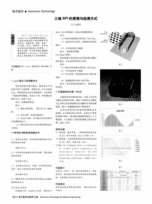
图 2
( 1 )激 光 分 辨 半 低 , 一 般 仃 1 0— 2 0 u n r
级
8b i t 灰 阶
( P MP ) ,8比 特 的 荻 阶 分 辨 率 , 达 到 O . 3 7微 米 ( 2 ) 单次 采 样 ,重 复 性 精 度 低 。 ( 3 )运 动 t t t 采样 , 外 界 震 动 及 传 动 震 动 的检 测 分 辨 率 ,相 比激 光 测 量 精 度 提 高 了 2个
E1 e ct r0ni C S S Y st eI l l i nt e g r at i on
s 0 楫 乜
T e c h no1 o gY Co n f er e n c e
1 J 4 0 .
( I EE E ). 1 1 3 5 — 图 4
0
0 t 一
{ l
I l x
i. / / /
/ 一 ///
6
橱曩
90 柑恕 J 2 0 相
5 0 整 } H
2 . 2 利 用 结 构 光 栅 的 灰 度 变化 测 量 度 的 高度 值
r h e 01 0 gi C a 1 b e h a v i 0 r [ C] . 2 n d
0f S 01 d e r Pa st e C 0mP01 1 C nt s o 1 1
图 3
2 P M P 相 位 调 制 轮 廓测 量 技 术
2 . 1 使 用 白 色光 源 、 通 过 结 构 光 栅 的 相位 变化
对 焊 膏进 行 测 量
电子技术 ・ E l e c t r o n i c T e c h n o l o g y
SPI操作手册编程指南
(按顺时针方向
打开电脑电源开关,并由。
装置将自动做初始化处理。
打开后图形显示
删除选中的线和焊盘
删除选中的线和焊盘
删除选中的线和焊盘
4.1.5自动拼板
4.2.3打开文件
找到所需的.mdb文件,点击“打开”按钮,则进入下图:
4.2.4按钮介绍
打开文件保存文件
逆时间旋转顺时间选择
X镜像Y镜像
删除选中焊盘检测选中焊盘
不检测选中焊盘选择所有焊盘
不选择焊盘反选焊盘
,完成后再重复做其余的
选中右侧值设定中的项目左侧对应的变为可修改,然后可以设置选中项目的参数。
4.2.6路径优化。
4.2.7板尺寸类型设置
点击工具进到板尺寸类型界面
4.3.2打开JOB文件
点击打开跳出选择界面
选择之前做好的程序,点击打开
4.3.3机器启动
按下装置绿色运行开关,装置绿色运行指示灯变亮,主界面上安全门状态显示绿底白字的字样。
4.3.4机器归零
选择归零后机台状态为回零,当机器状态变成等候时回零结束打开基准点,选择调整同步点后出现下图
在1中将基准点移至第一个基准点处,在FOV显示中会有显示。
(在1和FOV显示中,鼠标单击某个点,相机中心会到选择的点)移动完成后选择确定
选择出现下图然后选择抽锡膏出现下图
通过调整RGB三种光的参数,让黄色区域基本覆盖锡球所在区域
然后点击应用出现下图
确认Save PadID records的数量是否是全部焊盘的数量,确认OK后点击确定,然后再点击保存,保存完后点击关闭,这样程序就做好了。
变暗。
变暗。
SPis03 说明书
3) 器件配置字 ..................................................................................................................................................14 4) 器件信息 ......................................................................................................................................................14 5) 量产模式 ......................................................................................................................................................14 3.2.4 编程,将缓冲区的数据烧录到芯片中.................................................... 14 3.2.5 安全性与密码输入.................................................................... 15
2.1.1 从随机的 CD-ROM 盘上安装.............................................................. 3 2.1.2 从 Internet 网上下载安装软件(推荐).................................................... 3 2.1.3 软件安装过程 (以 SUPERPRO/IS03 为例).................................................. 3 2.1.4 连接硬件和驱动程序的安装............................................................. 8 2.1.5 运行编程器应用软件................................................................... 8
SPI工具说明书
SPI工具使用说明
一、打开软件,界面如下:
二、选择芯片,可根据厂商选择,也可以直接输入型号查找。
选择芯片后信息框中显示了所选芯片的厂商、型号、芯片容量。
注:SPI不支持OTP(One Time Programable,一次性可编程)存储区的烧录,所以软件也不处理25系列芯片OTP(One Time Programable,一次性可编程)存储区的数据,请用户注意。
三、点击“选择文件”,选择要处理的BIN文件。
打开后,信息框显示文件路径。
四、点击“处理文件”,将会生成和芯片名称相同的ver和bin 文件,并放在SPI.EXE所在目录下。
将新生成的文件拷贝到SD卡即可。
最新3shape说明书资料
1安装1确保扫描仪开关为“关”.2将鼠标和键盘连接到电脑下部的USB端口。
3打开/启动电脑4将加密狗密匙插入电脑下部的一个USB插口中。
5将扫描仪连接到电脑的一个USB2.0端口。
6将扫描仪连接到电源,并将电源连接到电源插座。
7打“开”扫描仪。
现在,您必须按照下页中的说明校准扫描仪2校准1将扫描工具包配件盒放在扫描仪附近伸手可及的地方。
2点击您桌面上的ScanServer,启动快捷图标以激活扫描服务器。
3点击出现在任务栏上的ScanServer按钮。
4按“校准扫描仪”按钮。
5依照您屏幕上的说明执行扫描仪校准。
当系统要求时,插入“扫描工具包的校准点盘”和“校准方块”。
以下指南将指引您执行完成修复件订单的必要步骤,从订单创建,到扫描、设计和以电子方式分配进行制造。
在我们的示例中,您将会创建一个基本的内冠。
3创建一笔订单1开始Dentail Manager(tm)-点击桌面的快捷图标。
2开始一笔新的订单-点击菜单栏内的新订单图标。
3输入订单信息-亦即在订单表格中输入技工所、客户、患者、订单设置等。
在此示例中,您可以输入虚拟的信息或者暂时在字段留下空白离开。
4选择修复齿-在订单详细信息下选择您想要设计修复的牙齿。
5选择适用范围-在订单详细信息下,选择框架。
其他说明,请按《F1》。
6选择材料和制造商-为您选择的默认材料和制造商。
如果您想加以更改,点击加号按钮“+”,再从列表中选择。
7下一步-点击扫描按钮开始扫描应用程序:ScanIt Restoration(tm)。
4扫描以下说明描述利用我们的示例单内冠扫描模型的方式。
请参阅在线帮助,了解完整的牙科适用范围的扫描说明,包括印模扫描。
1设备代型-讲扫描粘土放在扫描板中央,将代型固定到粘土上。
2讲代型插入扫描仪中-打开扫描仪门,并将板代型种植牙钉插入扫描仪内。
将板的三个底钉与扫描器床中三个相对应的孔对齐。
关闭扫描仪门。
3开始扫描-点击ScanIt Restoration(tm)屏幕的下一步按钮开始扫描。
- 1、下载文档前请自行甄别文档内容的完整性,平台不提供额外的编辑、内容补充、找答案等附加服务。
- 2、"仅部分预览"的文档,不可在线预览部分如存在完整性等问题,可反馈申请退款(可完整预览的文档不适用该条件!)。
- 3、如文档侵犯您的权益,请联系客服反馈,我们会尽快为您处理(人工客服工作时间:9:00-18:30)。
实际操作流程
1.点击桌面上的e-SPIre
2.打开需要测试的文件并点击开始。
文件格式是以JBN为后缀的。
3.让板子进入机器等板子到达停板位置并夹紧会出现MARK 点错误的报警,消除报警后按下停止按钮,点击基准点选择调整同步点。
4.点击移动,后点击导航。
5.点击导航后出现下面的界面将相机移动到第一个MARK点的位置也就是显示的图片中可以看到第一个MARK点,如果亮度不够,可以调节亮度的大小与切换灯光。
最后点击确定。
6. 调节亮度的大小与切换灯光在界面中让MARK点是亮点且周围尽量不出现亮点。
然后自动居中。
也可以更改搜索范围。
7.钩选模板更新,将相似度更改为60以上,点击应用选择ALL 点击OK然后保存。
8.点击+查看其他MARK点并进行相似度测试。
测试通过后关闭窗口。
注意所有的MARK点都要在绿色的搜索范围以内。