MAX4376-MAX4377-MAX4378高边电流检测
基于max4172的电流检测电路设计与实现

基于max4172的电流检测电路设计与实现
《基于MAX4172的电流检测电路设计与实现》
电流检测是电子设备中常见的功能之一,它能够实时监测电路中的电流变化并提供反馈,以便及时调整电路工作状态。
基于MAX4172的电流检测电路是一种常用的设计方案,本文将介绍如何设计并实现这样一种电路。
MAX4172是一款精密电流检测放大器,具有高精度和低功耗的特点,因此非常适合用于电流检测电路的设计。
在设计电流检测电路时,首先需要选择合适的电流检测范围,然后根据所选范围选择合适的电流检测放大器。
MAX4172可提供多种增益范围的选择,因此可以满足不同范围电流的检测需求。
设计电流检测电路时,需要考虑电路的精度、稳定性和抗干扰能力。
MAX4172具有高精度和低温漂特性,能够提供稳定的输出,并具有较强的抗干扰能力,能够满足电子设备在复杂环境下的工作要求。
此外,MAX4172还具有低功耗和小封装体积的特点,使得它在电子设备中的应用更加灵活方便。
在实现电流检测电路时,除了选择合适的电流检测放大器外,还需要考虑电路的稳定性和可靠性。
通过合理布局电路和选择优质的元器件,可以有效提高电路的稳定性和可靠性。
此外,对于需要远距离传输电流检测信号的应用场景,还可以添加适当的滤波电路和保护电路,以确保信号的完整性和安全性。
综上所述,基于MAX4172的电流检测电路设计与实现是一项关键的工作,通过选用合适的电流检测放大器、合理设计电路和加强稳定性与可靠性的控制,可以实现一个高精度、高稳定性的电流检测电路,满足不同电子设备的需求。
西门子变频器M430说明书
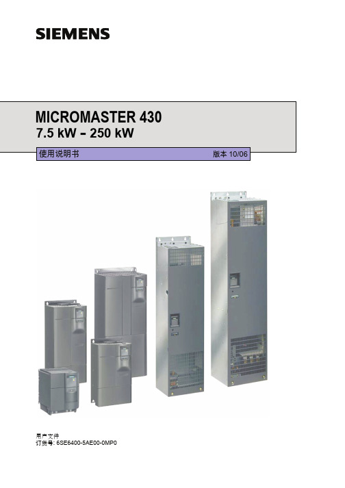
MICROMASTER 430
7.5 kW - 250 kW
使用说明书
版本 10/06
有关调试的
警告
!
¾ 未经培训合格的人员在变频器的器件/系统上工作或不遵守“警告”中的有关规定,就可能造
成严重的人身伤害或重大的财产损失。只有在设备的设计、安装、调试和运行方面受过培训 的经过认证合格的专业人员才允许在本设备的器件/系统上进行工作。
¾ 输入电源线只允许永久性紧固连接。设备必须接地(按照 IEC 536 Class 1、NEC 和其它适用 的标准)。
有关维修的
警告
!
¾ 设备的维修只能由西门子公司的服务部门,西门子公司授权的维修中心或经过认证合格并得
到授权的人员进行,这些人员应当十分熟悉本说明书中提出的所有警告和操作步骤。
¾ 任何有缺陷的部件和器件都必须用相应的备件更换。
¾ 在打开设备进行维修之前,一定要断开电源。
有关拆卸和废品处理的
注意 ¾ 变频器的包装箱是可以重复使用的。请保管好包装箱以备将来使用或把它返还给制造商。 ¾ 易卸螺丝和快速插接器便于您拆卸设备的部件。您可以回收这些拆卸下来的部件,并根据地
是其第§8 节关于“带电部件上工作时允许的安全距离”的规定。实际操作时,应该使用适当 的电子器具。 ¾ 在安装和调试变频器之前,请您务必仔细阅读这些安全规则和警告,以及设备上粘贴的所有 警示标志。确保警示标志置于醒目的地方,并更换已经脱落或损坏的标志。
MICROMASTER 430 使用说明书
MAX9918/19/20:高边电流检测放大器
出的 FAN4174以及具 有双通道 的 FAN4274,为便携 和消
=GND时 ,这 三款 器 件工 作在 单 向放 大器 模式 ;VREF,N=
V。。/2瞄回目圄四
M axim w w w.m axim -ic.com
Fairchild W W Wofairchildsem Lcorn
世 界 电 子 元 器 件 201 0.5 gec.eccn.com _
11
采 用 ST新 系 统 级 芯 片
电的应 用 , 同时 也 适 合
的下一代 电视 ,可以实
需要小体积及高分辨率
现 引人注 目的电视服务
的 其他 位 置 检 测 应 用 。
和全 新的高价值 内容业 务模 式 ,电视观众 将获
AS5055集成 了 4个霍 尔 传 感 元 件 、1个 12
得 丰富多彩且直 观的使
位角度编 码器 、1个 智
用体 验 。
能电源管理控制器和 1个易于使用的 3线或4线 SPI通信接口。
新系列代号 为 Freeman,为性能和软件可升级 的系统
这款 低功 耗编码 器采 用小型 4mmx4mm QFN封装 ,
级 芯片 ,FLI7510是其 中首款 产 品 ,定位于 主流和 高端 数 根据读 出速率 ,电流消耗 降低到 了微安级 ,如每秒 1 0次测
字电视细分 市场 。此 外 ,FLI7510的设计能 够满足 绿色节 量平 均 50pA。
能消费电子设备日益严格的系统能耗标准。匿囡豳
编码器系统的组装 只需要少量片上无源元件和 1个旋转
ST M icroeIectronics ww w.stm icroelectronics.corn .cn
MAX44242 低输入偏置电流、低噪声操作放大器 (OP 放大器) 评估套件说明书

General DescriptionThe MAX44242 evaluation kit (EV kit) provides a prov-en design to evaluate the MAX44242 low-input biascurrent, low-noise operational amplifier (op amp) in an8-pin µMAX ® package. The EV kit circuit is preconfig-ured as noninverting amplifiers, but can be adapted toother topologies by changing a few components. Thecomponent pads accommodate 0805 packages, makingthem easy to solder and replace. The EV kit comes with aMAX44242AUA+ installed.Features and Benefits●Accommodates Multiple Op-Amp Configurations●Rail-to-Rail Outputs●Accommodates Easy-to-Use 0805 Components● 2.7V to 20V Single Supply or ±1.35V to Q 10V DualSupplies●Proven PCB Layout●Fully Assembled and TestedQuick StartRequired Equipment●MAX44242 EV kit●+5V, 10mA DC power supply (PS1)●Two precision voltage sources●Two digital multimeters (DMMs)Procedure The EV kit is fully assembled and tested. Follow the steps below to verify board operation:1) Verify that the jumpers are in their default position, as shown in Table 1.2) Connect the positive terminal of the +5V supply to VDD and the negative terminal to GND and VSS.3) Connect the positive terminal of the precision voltage source to INAP . Connect the negative terminal of the precision voltage source to GND.4) Connect INAM to GND.5) Connect the positive terminal of the second precision voltage source to the INBP pad. Connect the nega-tive terminal of the precision voltage source to GND.6) Connect INBM to GND.7) Connect the DMMs to monitor the voltages on OUTA and OUTB. With the 10kΩ feedback resistors and 1kΩ series resistors, the gain of each noninverting amplifier is +11.8) Turn on the +5V power supply.9) Apply 100mV from the precision voltage sources. Observe the output at OUTA and OUTB on the DMMs. Both should read approximately +1.1V.10) Apply 400mV from the precision voltage sources. Both OUTA and OUTB should read approximately +4.4V.19-6917; Rev 0; 2/14Ordering Information appears at end of data sheet.μMAX is a registered trademark of Maxim Integrated Products, Inc.Detailed Description of HardwareThe MAX44242 EV kit provides a proven layout for theMAX44242 low input bias current, low-noise dual op amp.The IC is a single-supply dual op amp whose primaryapplication is operating in the noninverting configuration;however, the IC can operate with a dual supply as long asthe voltage across the VDD and GND pins of the IC do notexceed the absolute maximum ratings. When operatingwith a single supply, short VSS to GND.Op-Amp Configurations The IC is a single-supply dual op amp ideal for differential sensing, noninverting amplification, buffering, and filter-ing. A few common configurations are shown in the next few sections.The following sections explain how to configure one of the device’s op amps (op-amp A). To configure the device’s second op amp (op-amp B), the same equations can be used after modifying the component reference designa-tors. For op-amp B, the equations should be modified by adding 10 to the number portion of the reference designa-tors (e.g., for the noninverting configuration, equation R1 becomes R11 and R5 becomes R15).Noninverting ConfigurationThe EV kit comes preconfigured as a noninvertingamplifier. The gain is set by the ratio of R5 and R1. TheEV kit comes preconfigured for a gain of +11. The outputvoltage for the noninverting configuration is given by the equation below:OUTA INAP R5V 1V R1 =+ *Default position.JUMPERSHUNT POSITION DESCRIPTION JU1Installed*Connects INAM to R1. Also shorts capacitor C5.OpenConnects INAM to R1 through capacitor C5. When AC-coupling is desired, remove the shunt and install capacitor C5. JU2Installed*Connects INAP to JU3 position 1. Also shorts capacitor C6. OpenConnects INAP to JU3 position 1 through capacitor C6. When AC-coupling is desired, remove the shunt and install capacitor C6. JU31-2*Connects INAP to JU2 and C6 through R2 and R82-3Connects INAP to GND through R2 and R8JU4Installed*Connects OUTA to OUTA OpenConnects OUTA to OUTA through capacitor C10. When AC-coupling is desired, remove the shunt and install capacitor C10. JU5Installed*Connects INBM to R11. Also shorts capacitor C15. OpenConnects INBM to R11 through capacitor C15. When AC-coupling is desired, remove the shunt and install capacitor C15. JU6Installed*Connects INBP to JU6 position 1. Also shorts capacitor C16. OpenConnects INBP to JU6 position 1 through capacitor C16. When AC-coupling is desired, remove the shunt and install capacitor C16. JU71-2*Connects INBP to JU7 and C16 through R12 and R182-3Connects INBP to GND through R12 and R18JU8Installed*Connects OUTB to OUTB Open Connects OUTB to OUTB through capacitor C20. When AC-coupling is desired, remove the shunt and install capacitor C20.R1–R3, and R5 with appropriate resistors. WhenR1 = R2 and R3 = R5, the CMRR of the differential ampli-fier is determined by the matching of the resistor ratiosR1/R2 and R3/R5.OUTA INAP INAM V GAIN (V V )=−where:R5R3GAIN R1R2==Sallen-Key Filter ConfigurationThe Sallen-Key filter topology is ideal for filtering sensorsignals with a second-order filter and acting as a buffer.Schematic complexity is reduced by combining the filterand buffer operations. The EV kit can be configured ina Sallen-Key topology by replacing and populating afew components. The Sallen-Key topology is typicallyconfigured as a unity-gain buffer, which can be done byreplacing R1 and R5 with 0Ω resistors and short JU2. Thenoninverting signal is applied to the INAP test point withJU2 short and short pins 1-2 on JU3 or do the same on theINBP pad similarly. The filter component pads are R2–R4,and R8, where some have to be populated with resistorsand others with capacitors.Lowpass Sallen-Key FilterTo configure the Sallen-Key as a lowpass filter, populatethe R2 and R8 pads with resistors, and populate the R3and R4 pads with capacitors. The corner frequency and Qare then given by:C R3R2R8f Q ==the R3 and R4 pads with resistors and populate the R2 and R8 pads with capacitors. The corner frequency and Qare then given by:C R4R2R8f Q ==Transimpedance Application To configure op-amp U1-A as a transimpedance amplifier (TIA), replace R1 with a 0Ω resistor and install a shunt on jumper JU1 and shunt on pins 2-3 on jumper JU3. The output voltage of the TIA is the input current multiplied by the feedback resistor:OUT IN BIAS OS V (I I )R4V =+×+where R4 is installed as a 10kΩ resistor, I IN is defined as the input current source applied at the INAM pad, I BIAS is the input bias current, and V OS is the input offset voltage of the op amp. Use capacitor C8 (and C7, if applicable) to stabilize the op amp by rolling off high-frequency gain due to a large cable capacitance. Similarly, we can configure op-amp U1-B for transimpedance application.Capacitive Loads Some applications require driving large capacitive loads. To improve the stability of the amplifier, replace R6 (R16 for U1-B) with a suitable resistor value to improve ampli-fier phase margin. The R6/C9 (R16/C19 for U1-B) filter can also be used as an anti-alias filter, or to limit amplifier output noise by reducing its output bandwidth.DESIGNATION QTY DESCRIPTIONC1, C320.1µF ±10%, 25V X7R ceramic capacitors (0805)C2, C424.7µF ±10%, 25V X5R ceramic capacitors (0805)C5–C10, C15–C200Not installed, ceramic capacitors(0805)GND2Black test points INAM, INAP,INBM, INBP,OUTA, OUTB,VDD, VSS8Red test pointsJU1, JU2,JU4–JU6, JU862-pin headers JU3, JU723-pin headers DESIGNATION QTY DESCRIPTION R1, R2,R11, R1241kΩ ±1% resistors (0805)R3, R4, R7,R13, R14, R170Not installed, resistors (0805) R5, R15210kΩ ±1% resistors (0805)R6, R8,R16, R1840Ω ±5% resistors (0805) TP1, TP20Not installed, miniature test points U11Dual low-power, rail-to-rail I/O opamp (8 µMAX)Maxim MAX44242AUA+—8Shunts—1PCB: MAX44242 EVKITFigure 1. MAX44242 EV Kit SchematicFigure 3. MAX44242 EV Kit PCB Layout—Component SideComponent SideFigure 4. MAX44242 EV Kit PCB Layout—Solder SidePART TYPE MAX44242EVKIT#EV Kit #Denotes ROHS compliant.Maxim Integrated cannot assume responsibility for use of any circuitry other than circuitry entirely embodied in a Maxim Integrated product. No circuit patent licenses are implied. Maxim Integrated reserves the right to change the circuitry and specifications without notice at any time.REVISIONNUMBERREVISION DATE DESCRIPTION PAGES CHANGED 02/14Initial release —For pricing, delivery, and ordering information, please contact Maxim Direct at 1-888-629-4642, or visit Maxim Integrated’s website at .。
MAX4376FAUK中文资料

GAIN
SUFFIX
20
T
50
F
100
H
For example, MAX4376TAUK is a single high-side amplifier with a gain of 20.
High-side current monitoring is especially useful in battery-powered systems since it does not interfere with the ground path of the battery charger. The input common-mode range of 0 to +28V is independent of the supply voltage and ensures that the current-sense feedback remains viable even when connected to a battery pack in deep discharge.
-40°C to +125°C -40°C to +125°C -40°C to +125°C -40°C to +125°C -40°C to +125°C -40°C to +125°C
5 SOT23-5 5 SOT23-5 5 SOT23-5 8 SO 8 SO 8 SO
ADOG ADOH ADOI
Applications
Notebook Computers
Current-Limited Power Supplies
Fuel Gauges in PC
General-System/BoardLevel Current Monitoring
Nsiway NNSS44335588 超低EMI、无需滤波器、5W+3W×2的2.1声道 用户手
10.1
TQFN4×4-28 封装尺寸................................................................................................................... 18
10.2
SOP-28 封装尺寸............................................................................................................................ 19
7.3
NS4358 引脚功能描述 ..................................................................................................................... 9
7.4
芯片印章说明 ................................................................................................................................. 10
NS4358
超低EMI、无需滤波器、5W+3W×2的2.1声道+3D环绕立体声数字音频功放
NS4358 用户手册 V1.1
深圳市纳芯威科技有限公司 2011 年 10 月
Nsiway
1
日期
2011-3-11 2011-10-11
NS4358
超低EMI、无需滤波器、5W+3W×2的2.1声道+3D环绕立体声数字音频功放
德州仪器MAX4372-MAX4372T 电流检测放大器 用户手册说明书

General DescriptionThe MAX4372 low-cost, precision, high-side current-sense amplifier is available in a tiny, space-saving SOT23 5-pin package. Offered in three gain versions (T = 20V/V, F = 50V/V, and H = 100V/V), this device oper-ates from a single 2.7V to 28V supply and consumes only 30μA. It features a voltage output that eliminates the need for gain-setting resistors and is ideal for today’s notebook computers, cell phones, and other systems where battery/ DC current monitoring is critical.High-side current monitoring is especially useful in bat-tery-powered systems since it does not interfere with the ground path of the battery charger. The input common-mode range of 0 to 28V is independent of the supply volt-age and ensures that the current-sense feedback remains viable even when connected to a 2-cell battery pack in deep discharge.The user can set the full-scale current reading by choos-ing the device (T, F, or H) with the desired voltage gain and selecting the appropriate external sense resistor. This capability offers a high level of integration and flex-ibility, resulting in a simple and compact current-sense solution. For higher bandwidth applications, refer to the MAX4173T/F/H data sheet.Applications●Power-Management Systems●General-System/Board-Level Current Monitoring●Notebook Computers●Portable/Battery-Powered Systems●Smart-Battery Packs/Chargers●Cell Phones●Precision-Current Sources Features●Low-Cost, Compact Current-Sense Solution●30μA Supply Current● 2.7V to 28V Operating Supply●0.18% Full-Scale Accuracy●0.3mV Input Offset Voltage●Low 1.5Ω Output Impedance●Three Gain Versions Available• 20V/V (MAX4372T)• 50V/V (MAX4372F)• 100V/V (MAX4372H)●High Accuracy +2V to +28V Common-Mode Range,Functional Down to 0V, Independent of SupplyVoltage●Available in a Space-Saving 5-Pin SOT23 Packageand 3 x 2 UCSP™ (1mm x 1.5mm) Package Ordering Information appears at end of data sheet.UCSP is a trademark of Maxim Integrated Products, Inc.19-1548; Rev 5; 5/11+Denotes lead(Pb)-free/RoHS-compliant package.T = Tape and reel.*Note: Gain values are as follows: 20V/V for the T version,50V/V for the F version, and 100V/V for the H version. Current-Sense Amplifier with Voltage OutputPin ConfigurationsOrdering InformationPARTTEMPRANGEPIN-PACKAGETOPMARK MAX4372T EUK+T-40°C to +85°C 5 SOT23ADIU MAX4372TESA+-40°C to +85°C8 SO—MAX4372TEBT+T-40°C to +85°C 3 x 2 UCSP ACXV CC , RS+, RS- to GND .........................................-0.3V to +30V OUT to GND ..........................................................-0.3V to +15V Differential Input Voltage (V RS+ - V RS-) .............................±0.3V Current into Any Pin .........................................................±10mA Continuous Power Dissipation (T A = +70°C)5-Pin SOT23 (derate 3.9mW/°C above +70°C) .......312.6mW 8-Pin SO (derate 7.4mW/°C above +70°C) ..............588.2mW 3 x 2 UCSP (derate 3.4mW/°C above +70°C) .........273.2mWOperating Temperature Range ...........................-40°C to +85°C Storage Temperature Range ............................-65°C to +150°C Lead Temperature (soldering, 10s) .................................+300°C Soldering Temperature (reflow) .......................................+260°C(V RS+ = 0 to 28V, V CC = 2.7V to 28V, V SENSE = 0V, R LOAD = 1MΩ, T A = T MIN to T MAX , unless otherwise noted. Typical values are at T A = +25°C.) (Note 1)Current-Sense Amplifier with Voltage OutputAbsolute Maximum RatingsStresses beyond those listed under “Absolute Maximum Ratings” may cause permanent damage to the device. These are stress ratings only, and functional operation of the device at these or any other conditions beyond those indicated in the operational sections of the specifications is not implied. Exposure to absolute maximum rating conditions for extended periods may affect device reliability.Electrical CharacteristicsPARAMETERSYMBOL CONDITIONSMIN TYPMAX UNITS Operating Voltage Range (Note 2)V CC 2.728V Common-Mode Input Range (Note 3)V CMR 028V Common-Mode Rejection CMR V RS+ > 2V85dB Supply Current I CC V RS+ > 2V, V SENSE = 5mV 3060μA Leakage CurrentI RS+, I RS-V CC = 0V, V RS+ = 28V 0.051.2μAInput Bias CurrentI RS+V RS+ > 2V 01μAV RS+ ≤ 2V -25+2I RS-V RS+ > 2V 02V RS+ ≤ 2V-50+2Full-Scale Sense Voltage (Note 4)V SENSEGain = 20V/V or 50V/V 150mV Gain = 100V/V 100Input Offset Voltage (Note 5)V OST A = +25°CV CC = V RS+ = 12V MAX4372_ESA 0.3±0.8mVMAX4372_EUK, _EBT 0.3±1.3T A = T MIN to T MAX V CC = V RS+ = 12VMAX4372_ESA ±1.1MAX4372_EUK, _EBT±1.9Full-Scale Accuracy (Note 5)V SENSE = 100mV, V CC = 12V,V RS+ = 12V, T A = +25°C (Note 7)±0.18±3%Total OUT Voltage Error (Note 6)V SENSE = 100mV, V CC = 12V,V RS+ = 12V (Note 7)±6V SENSE = 100mV, V CC = 28V,V RS+ = 28V (Note 7)±0.15±7V SENSE = 100mV, V CC = 12V,V RS+ = 0.1V (Note 7)±1±28V SENSE = 6.25mV, V CC = 12V,V RS+ = 12V (Note 8)±0.15(V RS+ = 0 to 28V, V CC = 2.7V to 28V, V SENSE = 0V, R LOAD = 1MΩ, T A = T MIN to T MAX , unless otherwise noted. Typical values are at T A = +25°C.) (Note 1)Note 1: All devices are 100% production tested at T A = +25°C. All temperature limits are guaranteed by design.Note 2: Guaranteed by PSR test.Note 3: Guaranteed by OUT voltage error test.Note 4: Output voltage is internally clamped not to exceed 12V.Note 5: V OS is extrapolated from the gain accuracy tests.Note 6: Total OUT voltage error is the sum of gain and offset voltage errors.Note 7: Measured at I OUT = -500μA (R LOAD = 4kΩ for gain = 20V/V, R LOAD = 10kΩ for gain = 50V/V, R LOAD = 20kΩ for gain = 100V/V).Note 8: 6.25mV = 1/16 of 100mV full-scale voltage (C/16).Note 9: The device does not reverse phase when overdriven.Current-Sense Amplifier with Voltage OutputElectrical Characteristics (continued)PARAMETERSYMBOL CONDITIONSMINTYP MAXUNITSOUT Low Voltage(MAX4372T, MAX4372F)V OLV CC = 2.7V,V SENSE = -10mV, V RS+ = 28V I OUT = 10μA 2.6mVI OUT = 100μA 965OUT Low Voltage (MAX4372H)V OLV CC = 2.7V,V SENSE = -10mV, V RS+ = 12VI OUT = 10μA 2.6mVI OUT = 100μA965OUT High VoltageV CC - V OHV CC = 2.7V, I OUT = -500μA, V SENSE = 250mV, V RS+ = 28V0.10.25V-3dB Bandwidth BWV RS+ = 12V,V CC = 12V,C LOAD = 10pFV SENSE = 20mV,gain = 20V/V275kHzV SENSE = 20mV,gain = 50V/V 200V SENSE = 20mV,gain = 100V/V 110V SENSE = 6.25mV50GainMAX4372T20V/VMAX4372F 50MAX4372H100Gain AccuracyV SENSE = 20mV to 100mV, V R S + = 12V T A = +25°C ±0.25±2.5%T A = -40°C to +85°C ±5.5OUT Settling Time to 1% of Final ValueGain = 20V/V, V CC = 12V, V RS+ = 12V, C LOAD = 10pFV SENSE = 6.25mV to 100mV20µsV SENSE = 100mV to 6.25mV20Capacitive-Load Stability No sustained oscillations1000pF OUT Output Resistance R OUT V SENSE = 100mV 1.5ΩPower-Supply Rejection PSRV OUT = 2V, V RS+ > 2V7585dB Power-Up Time to 1% of Final ValueV CC = 12V, V RS+ = 12V,V SENSE = 100mV, C LOAD = 10pF 0.5ms Saturation Recovery Time (Note 9)V CC = 12V, V RS+ = 12V, C LOAD = 10pF0.1ms(V CC = 12V, V RS+ = 12V, V SENSE = 100mV, T A = +25°C, unless otherwise noted.)Current-Sense Amplifier with Voltage OutputTypical Operating Characteristics25.027.530.032.535.0SUPPLY CURRENT vs. SUPPLY VOLTAGESUPPLY VOLTAGE (V)S U P P L Y C U R R E N T (µA )121648202428-1.2-0.8-1.0-0.2-0.4-0.60.40.200.6010515202530TOTAL OUTPUT ERROR vs. SUPPLY VOLTAGESUPPLY VOLTAGE (V)O U T P U T E R R O R (%)00.20.40.60.81.01.21.41.610515202530TOTAL OUTPUT ERROR vs. COMMON-MODE VOLTAGECOMMON-MODE VOLTAGE (V)O U T P U T E R R O R (%)510152025303540-401060-153585SUPPLY CURRENT vs. TEMPERATURETEMPERATURE (°C)S U P P L Y C U R R E N T (µA )-1.0-0.50.501.01.5010050150200250300TOTAL OUTPUT ERROR vs. V SENSEV SENSE (mV)O U T P U T E R R O R (%)-1.0-0.9-0.8-0.7-0.6-0.5-0.4-0.3-0.2-0.10GAIN ACCURACY vs. TEMPERATURETEMPERATURE (°C)G A I N A C C U R A C Y (%)-401060-15358528.029.028.530.029.531.531.030.532.0SUPPLY CURRENTvs. COMMON-MODE VOLTAGECOMMON-MODE VOLTAGE (V)S U P P L Y C U R R E N T (µA )-45-90100100k10k 1k POWER-SUPPLY REJECTIONvs. FREQUENCY-75-85-55-65-40-70-80-50-60M A X 4372T t o c 06FREQUENCY (Hz)P S R (d B )-1.0-0.8-0.6-0.4-0.200.20.40.60.81.0-401060-153585TOTAL OUTPUT ERROR vs. TEMPERATURETEMPERATURE (°C)T O T A L O U T P U T E R R O R (%)(V CC = 12V, V RS+ = 12V, V SENSE = 100mV, T A = +25°C, unless otherwise noted.)Current-Sense Amplifier with Voltage OutputTypical Operating Characteristics (continued)V OUTV SENSE600mV200mV30mV10mV MAX4372TSMALL-SIGNAL TRANSIENT RESPONSEMAX4372T toc1020µs/div V OUTV SENSE1V3V50mV 150mV MAX4372TLARGE-SIGNAL TRANSIENT RESPONSEMAX4372T toc1320µs/divV OUTV SENSE 010V0100mV MAX4372HLARGE-SIGNAL TRANSIENT RESPONSE20µs/divMAX4372T toc15V OUTV SENSE2.5V7.5V50mV 150mVMAX4372FLARGE-SIGNAL TRANSIENT RESPONSE20µs/divMAX4372T toc143-81k100k10k1MSMALL-SIGNAL GAIN vs. FREQUENCY-7FREQUENCY (Hz)G A I N (d B)-6-5-4-3-2-1012V OUTV SENSE 1.5V0.5V30mV 10mVMAX4372FSMALL-SIGNAL TRANSIENT RESPONSEMAX4372T toc1120µs/div V OUTV SENSE 3V1V30mV10mV MAX4372HSMALL-SIGNAL TRANSIENT RESPONSEMAX4372T toc1220µs/divDetailed DescriptionThe MAX4372 high-side current-sense amplifier features a 0 to 28V input common-mode range that is indepen-dent of supply voltage. This feature allows the monitoring of current flow out of a battery in deep discharge, and also enables high-side current sensing at voltages far in excess of the supply voltage (V CC).Current flows through the sense resistor, generating a sense voltage (Figure 1. Functional Diagram). Since A1’s inverting input is high impedance, the voltage on the negative terminal equals V IN - V SENSE. A1 forces its positive terminal to match its negative terminal; therefore, the voltage across R G1 (V IN - V1-) equals V SENSE. This creates a current to flow through R G1 equal to V SENSE/ R G1. The transistor and current mirror amplify the current by a factor of β. This makes the current flowing out of the current mirror equal to:I M = β V SENSE/R G1A2’s positive terminal presents high impedance, so this current flows through R GD, with the following result:V2+ = R GD β x V SENSE/R G1R1 and R2 set the closed-loop gain for A2, which ampli-fies V2+, yielding:V OUT = R GD x β x V SENSE/R G1 (1 + R2/R1)The gain of the device equals:OUT SEN G1SE RGD x (1 + R2/R1)V V/Rβ=Applications Information Recommended Component ValuesThe MAX4372 operates over a wide variety of current ranges with different sense resistors. Table 1 lists com-mon resistor values for typical operation of the MAX4372.Choosing R SENSEGiven the gain and maximum load current, select R SENSE such that V OUT does not exceed V CC - 0.25V or 10V. To measure lower currents more accurately, use a high value for R SENSE. A higher value develops a higher sense volt-age, which overcomes offset voltage errors of the internal current amplifier.In applications monitoring very high current, ensure R SENSE is able to dissipate its own I2R losses. If the resistor’s rated power dissipation is exceeded, its value may drift or it may fail altogether, causing a differential voltage across the terminals in excess of the absolute maximum ratings.Figure 1. Functional DiagramCurrent-Sense Amplifier with Voltage OutputPin/Bump DescriptionPIN BUMPNAME FUNCTIONSOT23SO UCSP13A2GND Ground24A3OUT Output Voltage. V OUT is proportional to the magnitude of V SENSE (V RS+ - V RS-).31A1V CC Supply Voltage. Use at least a 0.1μF capacitor to decouple V CC from fast transients.48B1RS+Power Connection to the External Sense Resistor56B3RS-Load-Side Connection to the External Sense Resistor —2, 5, 7—N.C.No Connection. Not internally connected.Using a PC Board Trace as R SENSEIf the cost of R SENSE is an issue and accuracy is not criti-cal, use the alternative solution shown in Figure 2. This solution uses copper PC board traces to create a sense resistor. The resistivity of a 0.1in wide trace of 2oz copper is about 30mΩ/ft. The resistance temperature coefficient of copper is fairly high (approximately 0.4%/°C), so sys-tems that experience a wide temperature variance must compensate for this effect. In addition, self-heating intro-duces a nonlinearity error. Do not exceed the maximum power dissipation of the copper trace.For example, the MAX4372T (with a maximum load cur-rent of 10A and an R SENSE of 5mΩ) creates a full-scale V SENSE of 50mV that yields a maximum V OUT of 1V. R SENSE, in this case, requires about 2in of 0.1in wide copper trace.UCSP Applications InformationFor the latest application details on UCSP construction, dimensions, tape carrier information, printed circuit board techniques, bump-pad layout, and recommended reflow temperature profile, as well as the latest information on reliability testing results, go to the Maxim’s website at /ucsp to find the Application Note: UCSP—A Wafer-Level Chip-Scale Package.Figure 2. Connections Showing Use of PC BoardTable 1. Recommended Component ValuesCurrent-Sense Amplifier with Voltage OutputFULL-SCALE LOAD CURRENT,I LOAD (A)CURRENT-SENSERESISTOR,R SENSE (mΩ)GAIN(V/V)FULL-SCALE OUTPUTVOLTAGE (FULL-SCALEV SENSE = 100mV),V OUT (V)0.1100020 2.0 50 5.0 10010.0110020 2.0 50 5.0 10010.052020 2.0 50 5.0 10010.0101020 2.0 50 5.0 10010.0Current-Sense Amplifier with Voltage Output Ordering Information (continued)Pin Configurations (continued)PARTTEMPRANGEPIN-PACKAGETOPMARKMAX4372F EUK+T-40°C to +85°C 5 SOT23ADIV MAX4372FESA+-40°C to +85°C8 SO—MAX4372FEBT+T-40°C to +85°C 3 x 2 UCSP ACX MAX4372H EUK+T-40°C to +85°C 5 SOT23ADIW MAX4372HESA+-40°C to +85°C8 SO—MAX4372HEBT+T-40°C to +85°C 3 x 2 UCSP ACZChip InformationPROCESS: BiCMOS+Denotes lead(Pb)-free/RoHS-compliant package. T = Tape and reel.Current-Sense Amplifier with Voltage Output Package InformationFor the latest package outline information and land patterns (footprints), go to /packages. Note that a “+”, “#”, or “-” in the package code indicates RoHS status only. Package drawings may show a different suffix character, but the drawing pertains to the package regardless of RoHS status.PACKAGE TYPE PACKAGE CODE OUTLINE ND PATTERN NO.5 SOT23U5+121-005790-01748 SO S8+221-004190-00965 UCSP B6+221-0097—Note: MAX4372_EBT uses package code B6-2.Current-Sense Amplifier with Voltage Output Package Information (continued)For the latest package outline information and land patterns (footprints), go to /packages. Note that a “+”, “#”, or “-” in the package code indicates RoHS status only. Package drawings may show a different suffix character, but the drawing pertains to the package regardless of RoHS status.Current-Sense Amplifier with Voltage Output Package Information (continued)For the latest package outline information and land patterns (footprints), go to /packages. Note that a “+”, “#”, or “-” in the package code indicates RoHS status only. Package drawings may show a different suffix character, but the drawing pertains to the package regardless of RoHS status. Maxim Integrated │11Maxim Integrated cannot assume responsibility for use of any circuitry other than circuitry entirely embodied in a Maxim Integrated product. No circuit patent licenses are implied. Maxim Integrated reserves the right to change the circuitry and specifications without notice at any time. The parametric values (min and max limits) shown in the Electrical Characteristics table are guaranteed. Other parametric values quoted in this data sheet are provided for guidance.Maxim Integrated and the Maxim Integrated logo are trademarks of Maxim Integrated Products, Inc.Current-Sense Amplifier with Voltage Output© 2011 Maxim Integrated Products, Inc. │ 12Revision HistoryREVISIONNUMBERREVISION DATE DESCRIPTION PAGES CHANGED 47/09Updated feature in accordance with actual performance of the product 155/11Updated V RST conditions to synchronize with tested material and addedlead-free designation 1–3, 8For pricing, delivery, and ordering information, please contact Maxim Direct at 1-888-629-4642, or visit Maxim Integrated’s website at .。
高端电流检测放大器性能分析 MAX4372

高端电流检测放大器性能分析 MAX4372 MAX4173 MAX4080文章发布人:gxy 共193人阅读文字大小:[ 大中小 ] 文字背景色:在讨论器件功能时,检流放大器可以看作一个输入级浮空的仪表/差分放大器。
这意味着即使器件采用VCC=3.3V或5V单电源供电,在输入共模电压远高于电源电压的条件下,器件仍然能够正常放大差分输入信号。
检流放大器的共模电压可以很高,例如可以高达28V(MAX4372和MAX4173)或76V(MAX4080和MAX4081)。
检流放大器的这一特性使其非常适合高端电流检测应用,这类应用往往需要对高压侧检流电阻两端的微小电压进行放大,并馈入到低压ADC或低压模拟控制环路进行处理。
这种情况下,通常需要在信号源端(例如检流电阻两端)对电流检测信号进行滤波。
可以采用差分滤波器(图1)滤除负载电流和检流电压的“毛刺”,也可以采用共模滤波器(图2)以增强在出现共模电压尖峰或瞬时过压时的ESD 保护能力。
合理选择元件构建滤波器,如果元件选择不当,则会引入一些无法预知的失调电压和增益误差,降低电路性能。
滤波器的选择MAX4173检流放大器如图3所示,该器件的检流电阻可直接连接到芯片的RS+和RS-端。
器件内部的运算放大器将检流电阻两端的差分电压恢复成RG1两端的差分电压,即ILOAD×RSENSE=VSENSE=IRG1×RG1。
然后,内部电流镜对电流IRG1进行电平转换和放大,产生输出电流IRGD。
MAX4173的内部电路中RGD=12kΩ,而RG1=6kΩ。
因此,由于RGD和RG1为片上电阻,实际阻值会因不同的半导体工艺而产生多达±30%的差异。
但是,因为最终增益精度取决于RGD和RG1的比例,所以可以很好地控制增益,并在生产过程中灵活调整。
构建差分/共模滤波器(如图1和图2所示)时,需要在检流电阻的RSENSE+和RSENSE-端与器件的RS+和RS-引脚之间接入串联电阻,此时相当于改变了芯片的RG1和RG2。
- 1、下载文档前请自行甄别文档内容的完整性,平台不提供额外的编辑、内容补充、找答案等附加服务。
- 2、"仅部分预览"的文档,不可在线预览部分如存在完整性等问题,可反馈申请退款(可完整预览的文档不适用该条件!)。
- 3、如文档侵犯您的权益,请联系客服反馈,我们会尽快为您处理(人工客服工作时间:9:00-18:30)。
MAX4376/MAX4377/MAX4378 高边电流检测
该MAX4376/MAX4377/MAX4378 单,双和四精度高边电流检测放大器节省空间的封装。
它们的特点是缓冲电压输出,消除了对增益设置电阻
器的需要,并为今天的笔记本电脑,蜂窝电话的理想,并在目前的监测是至
关重要的其他系统。
这些精密设备提供三种固定增益为20,50 版本,和100
高边电流监测,特别是在电池供电系统非常有用,因为它不干扰地面
道路的电池充电器。
输入共模范围0 至+28 V 的电源电压是独立的,并确保电流检测反馈仍然是可行的,即使在连接到一个深度放电的电池组。
满量程电流值可以设置通过选择合适的电压增益和外部检测电阻。
这
种能力提供了集成性和灵活性高的水平,在一个简单和紧凑电流检测的解决
方案。
该MAX4376/MAX4377/MAX4378 工作在电源电压范围为+3 V 至+28 V,画出每个放大器的供应1mA 的电流,并在整个-40 度 C 汽车级温度范围内工作至+125 度 C 这些器件具有广泛的2MHz 的带宽,使它们成为内部电池充电器控制回路使用。
缓冲的输出驱动高达输出电流为2mA 成以地为参考的负载。
在MAX4376 可在一个很小的5 引脚SOT23 封装。
该
MAX4377/MAX4378 是节省空间的8 引脚μMAX®和14 引脚TSSOP 封装。