LLZ5241B中文资料
BTS5240L中文资料

TA = 85 °C
Vbb=12V, Tjstart=150°C;
(see diagrams on page 12)
IL = 6 A, EAS = 0.319 J, RL = 0 Ω,
one channel:
IL = 12 A, EAS = 0.679 J, RL = 0 Ω, two parallel channels:
Basic Functions
• Very low standby current • CMOS compatible input • Improved electromagnetic compatibility (EMC) • Stable behaviour at low battery voltage
Tj
-40...+150 °C
Storage temperature range
Tstg
-55...+150
Dynamical temperature rise at switching
dT
60
K
Power dissipation6) (DC), one channel active Maximal switchable inductance, single pulse
PCN 2004-018-A: BTS 5240L
Smart High-Sls: 2 x 25mΩ IntelliSense
Product Summary
Operating voltage
Vbb(on)
Active channels
On-state resistance Nominal load current Current limitation Low
ZD5245B资料

The ZD52XXBSG series covers zener voltage range from 2.4V to 33V, and is encapsulated in SOD-323 package, very suitable for low cost, low power voltage regulation application.
Forward Current (mA)
Forward Current (mA)
ZD5228B Forward Current vs Forward Voltage 350
300
250
200
150
100
50
0
0
200
400
600
800
1000 1200
Forward Voltage (mV)
ZD5229B Forward Current vs Forward Voltage 300
Spec. No. : C326SG Issued Date : 2003.06.30 Revised Date : Page No. : 5/13
1000
Forward Current (mA)
ZD5231B Forward Current vs Forward Voltage 300
LLZ5249B中文资料

Pb RoHSCOMPLIANCELLZ5221B – LLZ5263B500mW Hermetically Sealed Glass ZenerVoltage RegulatorsMINI MELFFeaturesZener voltage range 2.4 to 56 volts Mini-MELF packageSurface device type mounting Hermetically sealed glassCompression bonded construction All external surfaces are corrosionresistant and leads are readily solderable RoHS compliantMatte Tin (Sn) lead finishColor band indicates negative polarityDimensions in inches and (millimeters)Maximum Ratings and Electrical CharacteristicsRating at 25o C ambient temperature unless otherwise specified.Type NumberSymbol Value Units Power Dissipation Pd 500 mW Maximum Forward Voltage @ IF=200mA V F 1.1 VStorage Temperature Range T STG -65 to + 200 OCOperating Junction Temperature T J + 200 O CVersion: A07ELECTRICAL CHARACTERISTICS(TA=25O C unless otherwise noted)Z ZK @ I ZKDevice V z @ I zt Z ZT @ I ZT= 0.25mA I R @ V R(Volts)I ZTΩΩ(uA)V RNom mA Max Max Max Volts LLZ5221B 2.420301200100 1.0 LLZ5222B 2.520301250100 1.0 LLZ5223B 2.72030130075 1.0 LLZ5224B 2.82030140075 1.0 LLZ5225B 3.020******** 1.0 LLZ5226B 3.32028160025 1.0 LLZ5227B 3.62024170015 1.0 LLZ5228B 3.92023190010 1.0 LLZ5229B 4.320222000 5.0 1.0 LLZ5230B 4.720191900 5.0 2.0 LLZ5231B 5.120171600 5.0 2.0 LLZ5232B 5.620111600 5.0 3.0 LLZ5233B 6.020716900 5.0 3.5 LLZ5234B 6.22071000 5.0 4.0 LLZ5235B 6.8205750 3.0 5.0 LLZ5236B7.5206500 3.0 6.0 LLZ5237B8.2208500 3.0 6.5 LLZ5238B8.7208600 3.0 6.5 LLZ5239B9.12010600 3.07.0 LLZ5240B102017600 3.08.0 LLZ5241B112022600 2.08.4 LLZ5242B122030600 1.09.1 LLZ5243B139.5136000.59.9 LLZ5244B149.0156000.110 LLZ5245B158.5166000.111 LLZ5246B167.8176000.112 LLZ5247B167.4196000.113 LLZ5248B187.0216000.114 LLZ5249B19 6.6236000.114Version: A07ELECTRICAL CHARACTERISTICS(TA=25O C unless otherwise noted)Z ZK @ I ZKDevice V z @ I zt Z ZT @ I ZT= 0.25mA I R @ V R(Volts)I ZTΩΩ(uA)V RNom mA Max Max Max Volts LLZ5250B20 6.2256000.115 LLZ5251B22 5.6296000.117 LLZ5252B24 5.2336000.118 LLZ5253B25 5.0356000.119 LLZ5254B27 5.0416000.121 LLZ5255B28 4.5446000.121 LLZ5256B30 4.2496000.123 LLZ5157B33 3.8587000.125 LLZ5258B36 3.4707000.127 LLZ5259B39 3.2808000.130 LLZ5260B43 3.0939000.133 LLZ5261B47 2.710510000.136 LLZ5262B51 2.512511000.139 LLZ5263B56 2.215013000.143Notes: 1. The type numbers listed have zener voltage as shown and have a standard tolerance on the nominal zener voltae of ±5% in Blue marking, suffix A=±10%in Orange marking and D=±1% in Yellow marking.2. For detailed information on price, availability and deliver of nominal zener voltagesbetween the voltages shown and tighter voltage tolerances.3. The zener impedance is derived from the 60-cycle ac voltage, which results whenan ac current having an ms value equal to 10% of the dc zener current(I ZT or I ZK) is superimposed to I ZT or I ZK.Version: A07。
1N5248B-T中文资料

1N5221B - 1N5267B500mW EPITAXIAL ZENER DIODEFeaturesMaximum Ratings and Electrical Characteristics@ T A = 25°C unless otherwise specified·Case: DO-35·Case Material: Glass·Moisture Sensitivity: Level 1 per J-STD-020C ·Leads: Solderable per MIL-STD-202, Method 208·Terminals: Finish - Sn96.5Ag3.5. Solderable per MIL-STD-202, Method 208·Polarity: Cathode Band ·Marking: Type Number·Weight: 0.13 grams (approximate)·500mW Power Dissipation ·High Stability·Surface Mount Equivalents Available ·Hermetic Package·V Z - Tolerance ±5%·Lead Free Finish, RoHS Compliant (Note 2)Mechanical DataNotes:1. Valid provided that leads are kept at TL £75°C with lead length = 9.5mm (3/8”) from case; derate above 75°C.2.EC Directive 2002/95/EC (RoHS) revision 13.2.2003. Glass and High Temperature Solder Exemptions Applied where applicable,see EU Directive Annex Notes 5 and 7.Electrical Characteristics Table 1@ T A= 25°C unless otherwise specifiedNotes: 3. Based on dc measurement at thermal equilibrium; lead length = 9.5mm (3/8”); thermal resistance of heat sink = 30°C/W.Ordering Information(Note 5)Notes: 4. *Add "-A" or "-T" to the appropriate type number in Table 1. Example: 6.2V Zener= 1N5234B-A for ammo pack.5. For packaging details, visit our website at /datasheets/ap02008.pdf.IMPORTANT NOTICEDiodes Incorporated and its subsidiaries reserve the right to make modifications,enhancements,improvements,corrections or other changes without further notice to any product herein.Diodes Incorporated does not assume any liability arising out of the application or use of any product described herein;neither does it convey any license under its patent rights,nor the rights of others.The user of products in such applications shall assume all risks of such use and will agree to hold Diodes Incorporated and all the companies whose products are represented on our website,harmless against all damages.LIFE SUPPORTDiodes Incorporated products are not authorized for use as critical components in life support devices or systems without the expressed written approval of the President of Diodes Incorporated.。
MMBZ5231BL中文资料

MMBZ5221BLT1 SeriesPreferred DeviceZener Voltage Regulators 225 mW SOT−23 Surface MountThis series of Zener diodes is offered in the convenient, surface mount plastic SOT−23 package. These devices are designed to provide voltage regulation with minimum space requirement. They are well suited for applications such as cellular phones, hand held portables, and high density PC boards.Features•Pb−Free Packages are Available•225 mW Rating on FR−4 or FR−5 Board•Zener V oltage Range − 2.4 V to 91 V•Package Designed for Optimal Automated Board Assembly •Small Package Size for High Density Applications•ESD Rating of Class 3 (>16 KV) per Human Body Model Mechanical CharacteristicsCASE:V oid-free, transfer-molded, thermosetting plastic case FINISH:Corrosion resistant finish, easily solderableMAXIMUM CASE TEMPERATURE FOR SOLDERING PURPOSES: 260°C for 10 SecondsPOLARITY:Cathode indicated by polarity bandFLAMMABILITY RATING:UL 94 V−0MAXIMUM RATINGSMaximum ratings are those values beyond which device damage can occur. Maximum ratings applied to the device are individual stress limit values (not normal operating conditions) and are not valid simultaneously. If these limits are exceeded, device functional operation is not implied, damage may occur and reliability may be affected.1.FR−5 = 1.0 X 0.75 X 0.62 in.2.Alumina = 0.4 X 0.3 X 0.024 in, 99.5% alumina.Devices listed in bold, italic are ON Semiconductor Preferred devices. Preferred devices are recommended choices for future use and best overall value.ELECTRICAL CHARACTERISTICS(Pinout: 1-Anode, 2-No Connection, 3-Cathode) (T A = 25°C unless otherwise noted, V= 0.95 V Max. @ I = 10 mA)ZNOTE:MMBZ5233BLT1, MMBZ5246BLT1, MMBZ5251BLT1, and MMBZ5252BLT1 Not Available in 10,000/Tape & Reel.V Z , T E M P E R A T U R E C O E F F I C I E N T (m V /C )°θV Z , NOMINAL ZENER VOLTAGE (V)− 3− 2−1012345678Figure 1. Temperature Coefficients (Temperature Range −55°C to +150°C)V Z , T E M P E R A T U R E C O E F F I C I E N T (m V /C)°θ100101V Z , NOMINAL ZENER VOLTAGE (V)Figure 2. Temperature Coefficients (Temperature Range −55°C to +150°C)V Z , NOMINAL ZENER VOLTAGEFigure 3. Effect of Zener Voltage onZener ImpedanceZ Z T , D Y N A M I C I M P E D A N C E ()Ω1000100101V F , FORWARD VOLTAGE (V)Figure 4. Typical Forward VoltageI F , F O R W A R D C U R R E N T (m A )1000100101C , C A P A C I T A N C E (p F )V Z , NOMINAL ZENER VOLTAGE (V)Figure 5. Typical Capacitance 1000100101V Z , ZENER VOLTAGE (V)1001010.10.01I Z , Z E NE R C U R R E N T (m A )V Z , ZENER VOLTAGE (V)1001010.10.01I R , L E A K A G E C U R R E N T (A )µV Z , NOMINAL ZENER VOLTAGE (V)Figure 6. Typical Leakage Current10001001010.10.010.0010.00010.00001I Z , Z E N E R C U R R E N T (m A )Figure 7. Zener Voltage versus Zener Current(V Z Up to 12 V)Figure 8. Zener Voltage versus Zener Current(12 V to 91 V)PACKAGE DIMENSIONSSOT−23 (TO−236)CASE 318−08ISSUE AJ*For additional information on our Pb−Free strategy and solderingdetails, please download the ON Semiconductor Soldering and Mounting Techniques Reference Manual, SOLDERRM/D.SOLDERING FOOTPRINT*ǒmm inchesǓSCALE 10:1STYLE 8:PIN 1.ANODE2.NO CONNECTION3.CATHODEON Semiconductor and are registered trademarks of Semiconductor Components Industries, LLC (SCILLC). SCILLC reserves the right to make changes without further notice to any products herein. SCILLC makes no warranty, representation or guarantee regarding the suitability of its products for any particular purpose, nor does SCILLC assume any liability arising out of the application or use of any product or circuit, and specifically disclaims any and all liability, including without limitation special, consequential or incidental damages.“Typical” parameters which may be provided in SCILLC data sheets and/or specifications can and do vary in different applications and actual performance may vary over time. All operating parameters, including “Typicals” must be validated for each customer application by customer’s technical experts. SCILLC does not convey any license under its patent rights nor the rights of others. SCILLC products are not designed, intended, or authorized for use as components in systems intended for surgical implant into the body, or other applications intended to support or sustain life, or for any other application in which the failure of the SCILLC product could create a situation where personal injury or death may occur. Should Buyer purchase or use SCILLC products for any such unintended or unauthorized application, Buyer shall indemnify and hold SCILLC and its officers, employees, subsidiaries, affiliates,and distributors harmless against all claims, costs, damages, and expenses, and reasonable attorney fees arising out of, directly or indirectly, any claim of personal injury or death associated with such unintended or unauthorized use, even if such claim alleges that SCILLC was negligent regarding the design or manufacture of the part. SCILLC is an Equal Opportunity/Affirmative Action Employer. This literature is subject to all applicable copyright laws and is not for resale in any manner.PUBLICATION ORDERING INFORMATION。
MMBZ5241BLT1中文资料

225 mW SOT-23Zener Voltage Regulator DiodesGENERAL DATA APPLICABLE TO ALL SERIES IN THIS GROUPZener Voltage Regulator DiodesMAXIMUM CASE TEMPERATURE FOR SOLDERING PURPOSES: 260°C for 10 secondsTHERMAL CHARACTERISTICSCharacteristicSymbol Max Unit Total Device Dissipation FR-5 Board* P D225mW T A = 25°CDerate above 25°C1.8 mW/°C Thermal Resistance Junction to Ambient R θJA 556°C/W Total Device DissipationP D300mW Alumina Substrate,** T A = 25°C Derate above 25°C2.4mW/°C Thermal Resistance Junction to Ambient R θJA 417 °C/W Junction and Storage Temeprature T J , T stg150°C**FR-5 = 1.0 x 0.75 x 0.62 in.**Alumina = 0.4 x 0.3 x 0.024 in. 99.5% alumina.SEMICONDUCTORTECHNICAL DATAMMBZ5221BLT1SERIES 225mW SOT-23132CASE 318–07, STYLE 8SOT– 23 (TO–236AB)PLASTICELECTRICAL CHARACTERISTICS(Pinout: 1-Anode, 2-NC, 3-Cathode) (V F = 0.9 V Max @ I F = 10 mA for all types.)MMBZ5221BLT118A 20 2.41200301001MMBZ5222BLT118B 20 2.51250301001MMBZ5223BLT118C 20 2.7130030751MMBZ5224BLT118D 20 2.8140030751MMBZ5225BLT118E 203160029501MMBZ5226BLT18A 20 3.3160028251MMBZ5227BLT18B 20 3.617002415 1MMBZ5228BLT18C 20 3.9190023101MMBZ5229BLT18D 20 4.320002251MMBZ5230BLT18E 20 4.719001952MMBZ5231BLT18F 20 5.11600175 2MMBZ5232BLT18G 20 5.616001153MMBZ5233BLT18H 20 6160075 3.5MMBZ5234BLT18J 20 6.21000754MMBZ5235BLT18K 20 6.8750535MMBZ5236BLT18L 207.5500636MMBZ5237BLT18M 208.250083 6.5MMBZ5238BLT18N 208.760083 6.5MMBZ5239BLT18P 209.1600103 7MMBZ5240BLT18Q 2010600173 8MMBZ5241BLT18R 20116002228.4MMBZ5242BLT18S 2012 6003019.1MMBZ5243BLT18T 9.513600130.59.9MMBZ5244BLT18U 914600150.110MMBZ5245BLT18V 8.515600160.111MMBZ5246BLT18W 7.816600170.112MMBZ5247BLT18X 7.417600190.113MMBZ5248BLT1 8Y 718600210.114MMBZ5249BLT18Z 6.619600230.114MMBZ5250BLT181A 6.220600250.115MMBZ5251BLT181B 5.622600290.117MMBZ5252BLT181C 5.224600330.118MMBZ5253BLT181D 525 600350.119MMBZ5254BLT181E 4.627600410.121MMBZ5255BLT181F 4.528600440.121MMBZ5256BLT181G 4.230600490.123MMBZ5257BLT181H 3.833700580.125MMBZ5258BLT181J 3.436700700.127MMBZ5259BLT181K 3.239800800.130MMBZ5260BLT118F 343900930.1 33MMBZ5261BLT181M 2.74710001050.136MMBZ5262BLT181N 2.55111001250.1 39MMBZ5263BLT181P 2.25613001500.143MMBZ5264BLT181Q 2.16014001700.146MMBZ5265BLT181R 26214001850.147MMBZ5266BLT181S 1.86816002300.152MMBZ5267BLT181T 1.77517002700.156MMBZ5268BLT181U 1.58220003300.1 62MMBZ5269BLT181V 1.48722003700.1 68MMBZ5270BLT181W1.49123004000.169DeviceMarkingTest CurrentI ZT mAZener Voltage VZ(+5%)Nominal (Note1)Z Z kI Z =0.25mA ΩMaxZ Z kI Z =IZT@10%ModΩMaxMax I R @V R µAVNOTE 1. Zener voltage is measured with a pulse test current (I ZT ) applied at an ambient temperature of 25 °CGENERAL DATA - 225 mW SOT-23TYPICAL CHARACTERISICSGENERAL DATA — 225mW SOT –23876543210-1-2-323456789101112100101101001K1001011101000.40.50.60.70.80.91.01.11.2V Z , NOMINAL ZENER VOLTAGE (V)Figure 1. Temperature Coefficients (Temperature Range –55°C to +150°C)V Z , NOMINAL ZENER VOLTAGE (V)Figure 2. Temperature Coefficients (Temperature Range –55°C to +150°C)V Z , NOMINAL ZENER VOLTAGEFigure 3. Effect of Zener Voltage onZener ImpedanceV F , FORWARD VOLTAGE (V)Figure 4. Typical Forward Voltageθ V Z , T E M P E R A T U R E C O E F F I C I E N T (m V / °C )θ V Z , T E M P E R A T U R E C O E F F I C I E N T (m V / ° C )Z Z T , D Y N A M I C I M P E D A N C E (Ω)I F , F O R W A R D C U R R E N T (m A )V Z @ I ZTTYPICAL T C VALUES FOR MMBZ5221BLT1S E R I E STYPICAL T C VALUESFOR MMBZ5221BLT1S E R I E ST J = 25°CI Z(AC) = 0.1 I Z(DC)f = 1 kHzV Z @ I ZTI Z = 1 mA5 mA 20 mA1000100101150°C75 V (MMBZ5267BLT1)91 V (MMBZ5270BLT1)75°C 25°C0°CTYPICAL CHARACTERISICSGENERAL DATA — 225mW SOT –23100010010111010010001001010.10.010.0010.00010.0000101020304050607080901001010.1002468101210305070901001010.10.01BIAS AT 50% OF V Z NOMV Z , NOMINAL ZENER VOLTAGE (V)Figure 5. Typical Capacitance V Z , NOMINAL ZENER VOLTAGE (V)Figure 6. Typical Leakage CurrentV Z , ZENER VOLTAGE (V)Figure 7. Zener Voltage versus Zener Current(V Z Up to 12 V)V Z , ZENER VOLTAGE (V)Figure 8. Zener Voltage versus Zener Current(12 V to 91 V)T A = 25°C0 V BIAS 1 V BIAST A = 25°CT A = 25°C+150°C+25°C –55°CC , C A P A C I T A N C E (p F )I R , L E A K A G E C U R R E N T (µA )I Z , Z E N E R C U R R E N T (m A )I Z , Z E N E R C U R R E N T (m A )GENERAL DATA — 225 mW SOT-23225 mW SOT-23Zener Voltage Regulator Diodes — Surface MountedMULTIPLE PACKAGE QUANTITY (MPQ)REQUIREMENTSNOTES:1. DIMENSIONING AND TOLERANCING PER ANSI Y14.5M, 1982.2. CONTROLLING DIMENSION: INCH.3. MAXIMUM LEAD THICKNESS INCLUDES LEAD FINISH THICKNESS. MINIMUM LEAD THICKNESS IS THE MINIMUM THICKNESS OF BASE MATERIAL.A B C D G H J K L S VI N C H E S MILLIMETERS D I M M I N M A X M I N M A X 2.801.200.890.371.780.0130.0850.450.892.100.453.041.401.110.502.040.1000.1770.601.022.500.600.11020.04720.03500.01500.07010.00050.00340.01800.03500.08300.01770.11970.05510.04400.02000.08070.00400.00700.02360.04010.09840.0236(Refer to Section 10 for Surface Mount, Thermal Data and Footprint Information.)SOT-23 FootprintCASE 318-07PLASTICA LSVG123CKJB DHSTYLE 8:PIN 1. ANODE2. NO CONNECTION3. CATHODEmm inches ()0.0370.950.0370.950.0792.00.0350.90.0310.8(Refer to Section 10 for more information on Packaging Specifications.)Package Option Type No. SuffixMPQ (Units)T ape and Reel T13K Tape and AmmoT310K。
稳压管-MMSZ5245B
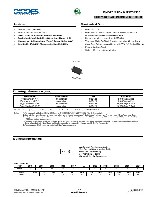
Features∙ 500mW Power Dissipation∙ General Purpose, Medium Current∙ Ideally Suited for Automated Assembly Processes∙ Totally Lead-Free & Fully RoHS Compliant (Notes 1 & 2) ∙ Halogen and Antimony Free. “Green” Device (Notes 3 & 4) ∙Qualified to AEC-Q101 Standards for High ReliabilityMechanical Data∙ Case: SOD123∙ Case Material: Molded Plastic, “Green” Molding Compound. UL Flammability Classification Rating 94V-0 ∙ Moisture Sensitivity: Level 1 per J-STD-020∙ Terminals: Matte Tin Finish Annealed over Alloy 42 Leadframe (Lead Free Plating). Solderable per MIL-STD-202, Method 208 ∙ Polarity: Cathode Band∙Weight: 0.01 grams (Approximate)Ordering Information (Note 5)*For (Type Number), please see the Electrical Characteristics Table. Example: 6.2V Zener = MMSZ5234B-7-F.Notes: 1. No purposely added lead. Fully EU Directive 2002/95/EC (RoHS) & 2011/65/EU (RoHS 2) compliant.2. See for more informati on about Diodes Incorporated’s definitions of Halogen - and Antimony-free, "Green" and Lead-free.3. Halogen- and Antimony-free "Green” products are defined as those which contain <900ppm bromine, <900ppm chlorine (<1500ppm total Br + Cl) and <1000ppm antimony compounds.4. Product manufactured with Date Code V9 (week 33, 2008) and newer are built with Green Molding Compound. Product manufactured prior to DateCode V9 are built with Non-Green Molding Compound and may contain Halogens or Sb 2O 3 Fire Retardants. 5. For packaging details, go to our website at .Marking InformationTop Viewxx = Product Type Marking Code(See Electrical Characteristics Table) YM = Date Code Marking Y = Year (ex: E = 2017)M = Month (ex: 9 = September)SOD123Maximum Ratings(@T A = +25°C, unless otherwise specified.)Thermal CharacteristicsElectrical Characteristics(@T A = +25°C, unless otherwise specified.)Notes: 4. RΘJL = 132°C/W5. Device mounted on FR-4 PCB with 1 inch copper pad layout.6. Short duration pulse test used to minimize self-heating effect.P , P O W E R D I S S I P A T I O N (W )D T, TEMPERATURE (C)Figure 1 Power Derating Curve°0102030405012345678910I , Z E N E R C U R R E N T (m A )Z V , ZENER VOLTAGE (V)Figure 2 Typical Zener Breakdown CharacteristicsZ2030I , Z E N E R C U R R E N T (m A )Z V , ZENER VOLTAGE (V)Figure 3 Typical Zener Breakdown Characteristics ZC , TO T A L C A P A C I T A N C E (p F )T 101001,000101001V , NOMINAL ZENER VOLTAGE (V)Figure 4 Typical Total Capacitance vs. Nominal Zener Voltage Z101001,000V , ZENER VOLTAGE (V)Figure 5 Typical Zener Impedance Characteristics Z Z , Z E N E R I M P E D AN C E ()Z-0.08-0.06-0.04-0.020V , ZENER VOLTAGE (V)Z Figure 6 Typical Temperature Coefficient of Zener Voltagevs. Zener Voltage (MMSZ5227B - MMSZ5258B)T C O F V , T E M P E R A T U R E C O E F F I C I E N T O F Z E N E R V O L T A G E (%/°C )ZPackage Outline DimensionsPlease see /package-outlines.html for the latest version.SOD123Suggested Pad LayoutPlease see /package-outlines.html for the latest version.SOD123。
WDZ-5241变压器差动保护装置要点
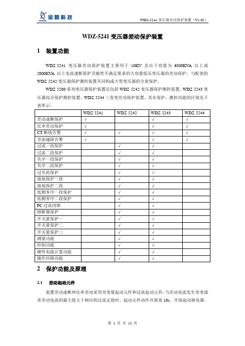
WDZ-5241变压器差动保护装置1装置功能WDZ-5241变压器差动保护装置主要用于10KV及以下容量为6300KV A以上或2000KV A以上电流速断保护灵敏性不满足要求的大容量低压变压器的差动保护,与配套的WDZ-5242变压器保护测控装置共同构成大型变压器的全套保护。
WDZ-5200系列变压器保护装置还包括WDZ-5242变压器保护测控装置、WDZ-5243变压器综合保护测控装置、WDZ-5244三卷变差动保护装置,其在保护、测控功能的区别见下表所示。
2保护功能及原理2.1差动起动元件装置差动速断和比率差动采用突变量起动元件和过流起动元件,当差动电流发生突变或者差动电流的最大值大于相应的过流定值时,起动元件动作并展宽10s,开放起动继电器。
2.2 差动电流制动电流计算公式按照同名端同在变压器侧或母线侧的原则,进行差动电流的计算,即为两侧电流的矢量和;制动电流按照两侧电流绝对值和的一半计算。
装置支持钟点数接线为YN,y/YN,d11/d,YN11/d,YN1,通过折算到高压侧的副边变比系数K phl 自动进行星三角转换,不需要通过外部转换。
额定二次值低侧额定一次值高侧高侧额定电压额定二次值高侧额定一次值低侧低侧额定电压CT CT CT CT ⨯⨯⨯⨯=phl K变压器钟点数为YN ,y :⎪⎪⎩⎪⎪⎨⎧⨯+=⎪⎭⎫⎝⎛⨯+=∙∙∙∙phl al ah a phl al ah a KI I DI K I I HI 2 ⎪⎪⎩⎪⎪⎨⎧⨯+=⎪⎭⎫ ⎝⎛⨯+=∙∙∙∙phl bl bh b phl bl bh b KI I DI K I I HI 2 ⎪⎪⎩⎪⎪⎨⎧⨯+=⎪⎭⎫ ⎝⎛⨯+=∙∙∙∙phl cl ch c phl cl ch c KI I DI K I I HI 2 式中: DI a 、DI b 、DI c :变压器A 、B 、C 差动电流HI a 、HI b 、HI c :变压器A 、B 、C 制动电流 I ah 、I bh 、I ch :变压器高压侧A 、B 、C 电流 I al 、I bl 、I cl :变压器低压侧A 、B 、C 电流变压器钟点数为YN ,d11:⎪⎪⎩⎪⎪⎨⎧⨯+⎪⎭⎫ ⎝⎛-=⎥⎦⎤⎢⎣⎡⨯+⎪⎭⎫ ⎝⎛-=∙∙∙∙∙∙phl al bh ah a phl al bh ah a KI I I DI K I I I HI 323⎪⎪⎩⎪⎪⎨⎧⨯+⎪⎭⎫ ⎝⎛-=⎥⎦⎤⎢⎣⎡⨯+⎪⎭⎫⎝⎛-=∙∙∙∙∙∙phl bl ch bh b phl bl ch bh b KI I I DI K I I I HI 323⎪⎪⎩⎪⎪⎨⎧⨯+⎪⎭⎫ ⎝⎛-=⎥⎦⎤⎢⎣⎡⨯+⎪⎭⎫⎝⎛-=∙∙∙∙∙∙∙phlcl ah ch c phl cl ah ch K I I I DI K I I I HIc 323变压器钟点数为d ,YN11:⎪⎪⎩⎪⎪⎨⎧⨯⎥⎦⎤⎢⎣⎡⎪⎭⎫ ⎝⎛-+=⎥⎦⎤⎢⎣⎡⨯⎪⎭⎫⎝⎛-+=∙∙∙∙∙∙phl cl al ah aphl cl al ah a KI I I DI K I I I HI 323 ⎪⎪⎩⎪⎪⎨⎧⨯⎥⎦⎤⎢⎣⎡⎪⎭⎫ ⎝⎛-+=⎥⎦⎤⎢⎣⎡⨯⎪⎭⎫⎝⎛-+=∙∙∙∙∙∙phl al bl bh bphl al bl bh b KI I I DI K I I I HI 323 ⎪⎪⎩⎪⎪⎨⎧⨯⎥⎦⎤⎢⎣⎡⎪⎭⎫ ⎝⎛-+=⎥⎦⎤⎢⎣⎡⨯⎪⎭⎫⎝⎛-+=∙∙∙∙∙∙phl bl cl ch cphl bl cl ch c KI I I DI K I I I HI 323 变压器钟点数为d ,YN1:⎪⎪⎩⎪⎪⎨⎧⨯⎥⎦⎤⎢⎣⎡⎪⎭⎫⎝⎛-+=⎥⎦⎤⎢⎣⎡⨯⎪⎭⎫⎝⎛-+=∙∙∙∙∙∙phl bl al ah aphl bl al ah a K I I I DI K I I I HI 323⎪⎪⎩⎪⎪⎨⎧⨯⎥⎦⎤⎢⎣⎡⎪⎭⎫⎝⎛-+=⎥⎦⎤⎢⎣⎡⨯⎪⎭⎫⎝⎛-+=∙∙∙∙∙∙phl cl bl bh bphl cl bl bh b K I I I DI K I I I HI 323⎪⎪⎩⎪⎪⎨⎧⨯⎥⎦⎤⎢⎣⎡⎪⎭⎫⎝⎛-+=⎥⎦⎤⎢⎣⎡⨯⎪⎭⎫⎝⎛-+=∙∙∙∙∙∙phl al cl ch cphl al cl ch c K I I I DI K I I I HI 3232.3 差动速断保护 2.3.1保护动作逻辑框图I da >I cdsdI dc >I cdsdI db >I cdsd 2.3.2保护动作判据cdsd I DI >max式中,I cdsd :差动速断保护动作电流整定值(A ) 2.4比率差动保护装置采用三折线比率差动原理,其动作曲线如下图所示,第3折线斜率固定为1。
- 1、下载文档前请自行甄别文档内容的完整性,平台不提供额外的编辑、内容补充、找答案等附加服务。
- 2、"仅部分预览"的文档,不可在线预览部分如存在完整性等问题,可反馈申请退款(可完整预览的文档不适用该条件!)。
- 3、如文档侵犯您的权益,请联系客服反馈,我们会尽快为您处理(人工客服工作时间:9:00-18:30)。
Pb RoHS
COMPLIANCE
LLZ5221B – LLZ5263B
500mW Hermetically Sealed Glass Zener
Voltage Regulators
MINI MELF
Features
Zener voltage range 2.4 to 56 volts Mini-MELF package
Surface device type mounting Hermetically sealed glass
Compression bonded construction All external surfaces are corrosion
resistant and leads are readily solderable RoHS compliant
Matte Tin (Sn) lead finish
Color band indicates negative polarity
Dimensions in inches and (millimeters)
Maximum Ratings and Electrical Characteristics
Rating at 25o C ambient temperature unless otherwise specified.
Type Number
Symbol Value Units Power Dissipation Pd 500 mW Maximum Forward Voltage @ IF=200mA V F 1.1 V
Storage Temperature Range T STG -65 to + 200 O
C
Operating Junction Temperature T J + 200 O C
Version: A07
ELECTRICAL CHARACTERISTICS(TA=25O C unless otherwise noted)
Z ZK @ I ZK
Device V z @ I zt Z ZT @ I ZT= 0.25mA I R @ V R
(Volts)I ZTΩΩ(uA)V R
Nom mA Max Max Max Volts LLZ5221B 2.420301200100 1.0 LLZ5222B 2.520301250100 1.0 LLZ5223B 2.72030130075 1.0 LLZ5224B 2.82030140075 1.0 LLZ5225B 3.020******** 1.0 LLZ5226B 3.32028160025 1.0 LLZ5227B 3.62024170015 1.0 LLZ5228B 3.92023190010 1.0 LLZ5229B 4.320222000 5.0 1.0 LLZ5230B 4.720191900 5.0 2.0 LLZ5231B 5.120171600 5.0 2.0 LLZ5232B 5.620111600 5.0 3.0 LLZ5233B 6.020716900 5.0 3.5 LLZ5234B 6.22071000 5.0 4.0 LLZ5235B 6.8205750 3.0 5.0 LLZ5236B7.5206500 3.0 6.0 LLZ5237B8.2208500 3.0 6.5 LLZ5238B8.7208600 3.0 6.5 LLZ5239B9.12010600 3.07.0 LLZ5240B102017600 3.08.0 LLZ5241B112022600 2.08.4 LLZ5242B122030600 1.09.1 LLZ5243B139.5136000.59.9 LLZ5244B149.0156000.110 LLZ5245B158.5166000.111 LLZ5246B167.8176000.112 LLZ5247B167.4196000.113 LLZ5248B187.0216000.114 LLZ5249B19 6.6236000.114
Version: A07
ELECTRICAL CHARACTERISTICS(TA=25O C unless otherwise noted)
Z ZK @ I ZK
Device V z @ I zt Z ZT @ I ZT= 0.25mA I R @ V R
(Volts)I ZTΩΩ(uA)V R
Nom mA Max Max Max Volts LLZ5250B20 6.2256000.115 LLZ5251B22 5.6296000.117 LLZ5252B24 5.2336000.118 LLZ5253B25 5.0356000.119 LLZ5254B27 5.0416000.121 LLZ5255B28 4.5446000.121 LLZ5256B30 4.2496000.123 LLZ5157B33 3.8587000.125 LLZ5258B36 3.4707000.127 LLZ5259B39 3.2808000.130 LLZ5260B43 3.0939000.133 LLZ5261B47 2.710510000.136 LLZ5262B51 2.512511000.139 LLZ5263B56 2.215013000.143
Notes: 1. The type numbers listed have zener voltage as shown and have a standard tolerance on the nominal zener voltae of ±5% in Blue marking, suffix A=±10%
in Orange marking and D=±1% in Yellow marking.
2. For detailed information on price, availability and deliver of nominal zener voltages
between the voltages shown and tighter voltage tolerances.
3. The zener impedance is derived from the 60-cycle ac voltage, which results when
an ac current having an ms value equal to 10% of the dc zener current
(I ZT or I ZK) is superimposed to I ZT or I ZK.
Version: A07。