KK74ACT20中文资料
74ACT11174DW资料

PACKAGING INFORMATIONOrderable Device Status (1)Package Type Package Drawing Pins Package Qty Eco Plan (2)Lead/Ball FinishMSL Peak Temp (3)74ACT11174DW OBSOLETE SOIC DW 20TBD Call TI Call TI 74ACT11174DWR OBSOLETE SOIC DW 20TBD Call TI Call TI 74ACT11174DWR OBSOLETE SOIC DW 20TBD Call TI Call TI 74ACT11174N OBSOLETE PDIP N 20TBD Call TI Call TI 74ACT11174NOBSOLETEPDIPN20TBDCall TICall TI(1)The marketing status values are defined as follows:ACTIVE:Product device recommended for new designs.LIFEBUY:TI has announced that the device will be discontinued,and a lifetime-buy period is in effect.NRND:Not recommended for new designs.Device is in production to support existing customers,but TI does not recommend using this part in a new design.PREVIEW:Device has been announced but is not in production.Samples may or may not be available.OBSOLETE:TI has discontinued the production of the device.(2)Eco Plan -The planned eco-friendly classification:Pb-Free (RoHS)or Green (RoHS &no Sb/Br)-please check /productcontent for the latest availability information and additional product content details.TBD:The Pb-Free/Green conversion plan has not been defined.Pb-Free (RoHS):TI's terms "Lead-Free"or "Pb-Free"mean semiconductor products that are compatible with the current RoHS requirements for all 6substances,including the requirement that lead not exceed 0.1%by weight in homogeneous materials.Where designed to be soldered at high temperatures,TI Pb-Free products are suitable for use in specified lead-free processes.Green (RoHS &no Sb/Br):TI defines "Green"to mean Pb-Free (RoHS compatible),and free of Bromine (Br)and Antimony (Sb)based flame retardants (Br or Sb do not exceed 0.1%by weight in homogeneous material)(3)MSL,Peak Temp.--The Moisture Sensitivity Level rating according to the JEDEC industry standard classifications,and peak solder temperature.Important Information and Disclaimer:The information provided on this page represents TI's knowledge and belief as of the date that it is provided.TI basesits knowledge and belief on information provided by third parties,and makes no representation or warranty as to the accuracy of such information.Efforts are underway to better integrate information from third parties.TI has taken and continues to take reasonable steps to provide representative and accurate information but may not have conducted destructive testing or chemical analysis on incoming materials and chemicals.TI and TI suppliers consider certain information to be proprietary,and thus CAS numbers and other limited information may not be available for release.In no event shall TI's liability arising out of such information exceed the total purchase price of the TI part(s)at issue in this document sold by TI to Customer on an annual basis.PACKAGE OPTION ADDENDUM24-Jun-2005Addendum-Page 1IMPORTANT NOTICETexas Instruments Incorporated and its subsidiaries(TI)reserve the right to make corrections,modifications,enhancements,improvements, and other changes to its products and services at any time and to discontinue any product or service without notice.Customers should obtain the latest relevant information before placing orders and should verify that such information is current and complete.All products are sold subject to TI’s terms and conditions of sale supplied at the time of order acknowledgment.TI warrants performance of its hardware products to the specifications applicable at the time of sale in accordance with TI’s standard warranty.Testing and other quality control techniques are used to the extent TI deems necessary to support this warranty.Except where mandated by government requirements,testing of all parameters of each product is not necessarily performed.TI assumes no liability for applications assistance or customer product design.Customers are responsible for their products and applications using TI components.To minimize the risks associated with customer products and applications,customers should provide adequate design and operating safeguards.TI does not warrant or represent that any license,either express or implied,is granted under any TI patent right,copyright,mask work right, or other TI intellectual property right relating to any combination,machine,or process in which TI products or services are rmation published by TI regarding third-party products or services does not constitute a license from TI to use such products or services or a warranty or endorsement e of such information may require a license from a third party under the patents or other intellectual property of the third party,or a license from TI under the patents or other intellectual property of TI.Reproduction of TI information in TI data books or data sheets is permissible only if reproduction is without alteration and is accompanied by all associated warranties,conditions,limitations,and notices.Reproduction of this information with alteration is an unfair and deceptive business practice.TI is not responsible or liable for such altered rmation of third parties may be subject to additional restrictions.Resale of TI products or services with statements different from or beyond the parameters stated by TI for that product or service voids all express and any implied warranties for the associated TI product or service and is an unfair and deceptive business practice.TI is not responsible or liable for any such statements.TI products are not authorized for use in safety-critical applications(such as life support)where a failure of the TI product would reasonably be expected to cause severe personal injury or death,unless officers of the parties have executed an agreement specifically governing such use.Buyers represent that they have all necessary expertise in the safety and regulatory ramifications of their applications,and acknowledge and agree that they are solely responsible for all legal,regulatory and safety-related requirements concerning their products and any use of TI products in such safety-critical applications,notwithstanding any applications-related information or support that may be provided by TI.Further,Buyers must fully indemnify TI and its representatives against any damages arising out of the use of TI products in such safety-critical applications.TI products are neither designed nor intended for use in military/aerospace applications or environments unless the TI products are specifically designated by TI as military-grade or"enhanced plastic."Only products designated by TI as military-grade meet military specifications.Buyers acknowledge and agree that any such use of TI products which TI has not designated as military-grade is solely at the Buyer's risk,and that they are solely responsible for compliance with all legal and regulatory requirements in connection with such use. TI products are neither designed nor intended for use in automotive applications or environments unless the specific TI products are designated by TI as compliant with ISO/TS16949requirements.Buyers acknowledge and agree that,if they use any non-designated products in automotive applications,TI will not be responsible for any failure to meet such requirements.Following are URLs where you can obtain information on other Texas Instruments products and application solutions:Products ApplicationsAmplifiers AudioData Converters AutomotiveDSP BroadbandClocks and Timers Digital ControlInterface MedicalLogic MilitaryPower Mgmt Optical NetworkingMicrocontrollers SecurityRFID TelephonyRF/IF and ZigBee®Solutions Video&ImagingWirelessMailing Address:Texas Instruments,Post Office Box655303,Dallas,Texas75265Copyright©2008,Texas Instruments Incorporated。
74ACTQ374SJ资料
元器件交易网www.cec源自74ACQ374 • 74ACTQ374
Logic Symbols
Functional Description
The ACQ/ACTQ374 consists of eight edge-triggered flipflops with individual D-type inputs and 3-STATE true outputs. The buffered clock and buffered Output Enable are common to all flip-flops. The eight flip-flops will store the state of their individual D-type inputs that meet the setup and hold time requirements on the LOW-to-HIGH Clock (CP) transition. With the Output Enable (OE) LOW, the contents of the eight flip-flops are available at the outputs. When the OE is HIGH, the outputs go to the high impedance state. Operation of the OE input does not affect the state of the flip-flops.
Ordering Code:
Order Number 74ACQ374SC 74ACQ374SJ 74ACQ374PC 74ACTQ374SC 74ACTQ374SJ 74ACTQ374QSC 74ACTQ374PC Package Number M20B M20D N20A M20B M20D MQA20 N20A Package Description 20-Lead Small Outline Integrated Circuit (SOIC), JEDEC MS-013, 0.300” Wide Body 20-Lead Small Outline Package (SOP), EIAJ TYPE II, 5.3mm Wide 20-Lead Plastic Dual-In-Line Package (PDIP), JEDEC MS-001, 0.300” Wide 20-Lead Small Outline Integrated Circuit (SOIC), JEDEC MS-013, 0.300” Wide Body 20-Lead Small Outline Package (SOP), EIAJ TYPE II, 5.3mm Wide 20-Lead Quarter Size Outline Package (QSOP), JEDEC MO-137, 0.150” Wide 20-Lead Plastic Dual-In-Line Package (PDIP), JEDEC MS-001, 0.300” Wide
74ACT00MTC中文资料
Device also available in Tape and Reel. Specify by appending suffix letter “X” to the ordering form. (PC not available in Tape and Reel.)
74HC20中文资料

AC CHARACTERISTICS FOR 74HC GND = 0 V; tr = tf = 6 ns; CL = 50 pF
Tamb (°C)
SYMBOL
PARAMETER
74HC
+25
−40 to +85
min. typ. max. min. max.
tPHL/ tPLH propagation delay
74HC/HCT20
Fig.4 Functional diagram. Fig.6 HCT logic diagram (one gate).
Fig.5 HC logic diagram (one gate).
FUNCTION TABLE
INPUTS
nA nB nC nD
L
X
X
X
X
L
X
X
X
X
L
X
X
X
Philips Semiconductors
Dual 4-input NAND gate
PIN DESCRIPTION
PIN NO. 1, 9 2, 10 3, 11 4, 12 5, 13 6, 8 7 14
74ACTQ14MTC资料
Note 1: Absolute maximum ratings are those values beyond which damage to the device may occur. The databook specifications should be met, without exception, to ensure that the system design is reliable over its power supply, temperature, and output/input loading variables. Fairchild does not recommend operation outside of databook specifications.
Recommended Operating Conditions
Supply Voltage (VCC) Input Voltage (VI) Output Voltage (VO) Operating Temperature (TA) 4.5V to 5.5 0V to VCC 0V to VCC −40°C to +85°C
Ordering Code:
Order Number 74ACTQ14SC 74ACTQ14MTC 74ACTQ14PC Package Number M14A MTC14 N14A Package Description 14-Lead Small Outline Integrated Circuit (SOIC), JEDEC MS-120, 0.150” Narrow Body 14-Lead Thin Shrink Small Outline Package (TSSOP), JEDEC MO-153, 4.4mm Wide 14-Lead Plastic Dual-In-Lead Package (PDIP), JEDEC MS-001, 0.300” Wide
KK74VHC00中文资料
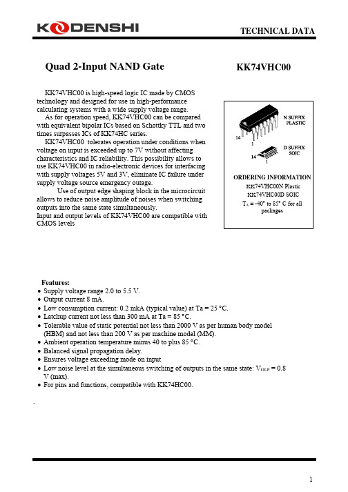
TECHNICAL DATAKK 74VHC00Quad 2-Input NAND GateKK 74VHC00 is high-speed logic IC made by CMOS technology and designed for use in high-performance calculating systems with a wide supply voltage range. As for operation speed, KK 74VHC00 can be compared with equivalent bipolar ICs based on Schottky TTL and two times surpasses ICs of KK 74НС series.KK 74VHC00 tolerates operation under conditions when voltage on input is exceeded up to 7V without affecting characteristics and IC reliability. This possibility allows to use KK 74VHC00 in radio-electronic devices for interfacing with supply voltages 5V and 3V, eliminate IC failure under supply voltage source emergency outage.Use of output edge shaping block in the microcircuit allows to reduce noise amplitude of noises when switching outputs into the same state simultaneously.Input and output levels of KK 74VHC00 are compatible with CMOS levelsFeatures:• Supply voltage range 2.0 to 5.5 V. • Output current 8 mA.• Low consumption current: 0.2 mkA (typical value) at Та = 25 °С. • Latchup current not less than 300 mA at Та = 85 °С.• Tolerable value of static potential not less than 2000 V as per human body model (HBM) and not less than 200 V as per machine model (ММ). • Ambient operation temperature minus 40 to plus 85°С. • Balanced signal propagation delay.• Ensures voltage exceeding mode on input• Low noise level at the simultaneous switching of outputs in the same state: V OLP = 0.8 V (max).• For pins and functions, compatible with KK 74НС00..KK74VHC00 truth tablePins description in KK74VHC00Absolute maximum conditions*Parameter, unit Symbol Valueminmax Supply voltage, V V CC-0.5 7.0Input voltage, V Vin -0.5 7.0Output voltage, V Vout -0.5 Vcc+0.5VInput diode current, mA Iik – -20Current of common output and supplyoutput, mAIcc – ± 75Output current, mA Iout – ± 25Output diode current, mA Iok – ± 20Dissipated power, mW Pd – 180*Under absolute maximum conditions operation of microcircuit is not guaranteed. Operation isguaranteed under maximum conditionsMaximum conditionsSymbol ValueParameter, unitminmax Supply voltage, V V CC 2.0 5.5Input voltage,V Vin 0 V CCOutput voltage, V Vout 0 V CCOutput current, mA Iout – ± 8.0Input rise and fall time, ns/V at Vcc = (3.3 ± 0.3) Vat Vcc = (5.0 ± 0.5) V t LH, t HL10020DC electrical characteristicsValue25 °C–40 to 85 °CSymbo l Parameter Test conditionsV CC ,V min max min maxUnit 2.01.5 – 1.5 – VV IHHigh input voltage–3.0-5.50.7Vcc– 0.7Vcc –2.0 – 0.5 – 0.5 V IL Low input voltage–3.0-5.5– 0.3Vcc – 0.3Vcc2.0 1.92– 1.9 –3.0 2.92– 2.9 –4.5 4.42– 4.4 – V I = V IH or V IL I O = -50 mkA5.5 5.52– 5.4 –V I = V IH or V IL ; I O = -4 mA3.0 2.58– 2.48 –V OHHigh output voltage V I = V IH or V IL ; I O = -8 mA4.5 3.94– 3.80 –2.0 – 0.09– 0.13.0 – 0.09– 0.14.5 – 0.09– 0.1 V I =V IH orV IL I O = 50 mkA 5.5 – 0.09– 0.1V I = V IH or V IL I O = 4 mA 3.0 – 0.36– 0.44V OLLow output voltage V I = V IH or V IL I O = 8 mA4.5 – 0.36– 0.44I OZ Output current in "off" stateV I = V IH or V IL V O = V CC or 0V 5.5 - ±0.25- ±2.5mkA I I Input current V I = 5.5V or 0V 0 – 5.5- ±0.1- ±1.0I CCConsumption current V I =V CC or 0V5.5 - 4.0 - 40.0AC electrical characteristics (t LH = t HL = 3.0 ns)Value25 °C–40to 85 °CSymbol Parameter Testconditi ons V CC , VC L , pF min max min maxUnit 15- 7.9- 9.5 3.3 ± 0.350 11.4 13.0 155.56.5 t PHL , t PLHPropagation delay time when switching "on", "off" Figure 2 5.0 ± 0.550 7.5 8.5ns C I Input capacity - 5.0 10 -C РDDynamic capacity V I = 0 V orV CC5.0 38 -pFNoise characteristics (C L = 50 pF)ValueSymbol Parameter V CC , V min maxUnit V OLP Positive noise of low output voltage 5.0 - 0.8 V V OLV Negative noise of low output voltage5.0 -0.8 - V IHD Input dynamic high voltage 5.0 3.5 - V ILDInput dynamic low voltage5.0-1.5- Time diagram of input and output pulsesVССGNDVCC0 V。
MM74HC20中文资料

2 A critical component is any component of a life support device or system whose failure to perform can be reasonably expected to cause the failure of the life support device or system or to affect its safety or effectiveness
Features
Y Y Y Y Y
Typical propagation delay 8 ns Wide power supply range 2 – 6V Low quiescent current 20 mA maximum (74HC Series) Low input current 1 mA maximum Fanout of 10 LS-TTL loads
TA e 25 C Typ
Units
Guaranteed Limits ns ns ns ns ns ns pF pF
tPHL tPLH
Maximum Propagation Delay Maximum Output Rise and Fall Time Power Dissipation Capacitance Note Maximum Input Capacitance
Max VCC
Units V V
a a
MC74ACT20D中文资料

FACT DATA 5-2
元器件交易网
MC74AC20 MC74ACT20
AC CHARACTERISTICS
74AC Symbol Parameter VCC* (V) Min tPLH tPHL Propagation Delay Propagation Delay 3.3 5.0 3.3 5.0 2.0 1.5 1.5 1.5 TA = +25°C CL = 50 pF Typ 6.0 5.0 5.0 4.0 Max 8.5 7.0 7.0 6.0 74AC TA = –40°C to +85°C CL = 50 pF Min 1.5 1.0 1.0 1.0 Max 10.0 8.0 9.0 7.0 ns ns Unit
1. Vin from 30% to 70% VCC; see individual Data Sheets for devices that differ from the typical input rise and fall times. 2. Vin from 0.8 V to 2.0 V; see individual Data Sheets for devices that differ from the typical input rise and fall times.
元器件交易网
MC74AC20 MC74ACT20 Dual 4 Input NAND Gate
• Outputs Source/Sink 24 mA • ′ACT20 Has TTL Compatible Inputs Pinout: 14-Lead Packages (Top View)
Guaranteed Limits 2.0 2.0 0.8 0.8 4.4 5.4 3.86 4.86 0.1 0.1 0.36 0.36 ±0.1 2.0 2.0 0.8 0.8 4.4 5.4 3.76 4.76 0.1 0.1 0.44 0.44 ±1.0 1.5 75 –75 40 V V V VOUT = 0.1 V or VCC – 0.1 V VOUT = 0.1 V or VCC – 0.1 V IOUT = – 50 µA *VIN = VIL or VIH – 24 mA IOH – 24 mA IOUT = 50 µA *VIN = VIL or VIH 24 mA IOH 24 mA VI = VCC, GND VI = VCC – 2.1 V VOLD = 1.65 V Max VOHD = 3.85 V Min VIN = VCC or GND
- 1、下载文档前请自行甄别文档内容的完整性,平台不提供额外的编辑、内容补充、找答案等附加服务。
- 2、"仅部分预览"的文档,不可在线预览部分如存在完整性等问题,可反馈申请退款(可完整预览的文档不适用该条件!)。
- 3、如文档侵犯您的权益,请联系客服反馈,我们会尽快为您处理(人工客服工作时间:9:00-18:30)。
TECHNICAL DATAKK 74ACT20Dual 4-Input NAND GateHigh-Speed Silicon-Gate CMOSThe KK 74ACT20 is identical in pinout to the LS/ALS20, HC/HCT20. The KK 74ACT20 may be used as a level converter for interfacing TTL or NMOS outputs to High Speed CMOS inputs. • TTL/NMOS Compatible Input Levels• Outputs Directly Interface to CMOS, NMOS, and TTL • Operating Voltage Range: 4.5 to 5.5 V• Low Input Current: 1.0 µA; 0.1 µA @ 25°C • Outputs Source/Sink 24 mALOGIC DIAGRAMPIN 14 =V CC PIN 7 = GNDPINS 3,11 = NO CONNECTIONPIN ASSIGNMENTNC = NO CONNECTIONFUNCTION TABLEInputs OutputA B C D Y L X X X H X L X X H X X L X H X X X L H H H H H LX = don’t careMAXIMUM RATINGS*Symbol Parameter ValueUnit V CC DC Supply Voltage (Referenced to GND) -0.5 to +7.0 VV IN DC Input Voltage (Referenced to GND) -0.5 to V CC +0.5 VV OUT DC Output Voltage (Referenced to GND) -0.5 to V CC +0.5 VI IN DC Input Current, per Pin ±20 mAI OUT DC Output Sink/Source Current, per Pin ±50 mAI CC DC Supply Current, V CC and GND Pins ±50 mAP D Power Dissipation in Still Air, Plastic DIP+ SOIC Package+ 750500mWTstg Storage Temperature -65 to +150 °CT L Lead Temperature, 1 mm from Case for 10 Seconds(Plastic DIP or SOIC Package)260 °C*Maximum Ratings are those values beyond which damage to the device may occur.Functional operation should be restricted to the Recommended Operating Conditions.+Derating - Plastic DIP: - 10 mW/°C from 65° to 125°CSOIC Package: : - 7 mW/°C from 65° to 125°CRECOMMENDED OPERATING CONDITIONSSymbol Parameter MinMaxUnit V CC DC Supply Voltage (Referenced to GND) 4.5 5.5 VV IN, V OUT DC Input Voltage, Output Voltage (Referenced to GND) 0 V CC VT J Junction Temperature (PDIP) 140 °CT A Operating Temperature, All Package Types -40 +85 °CI OH Output Current - High -24 mAI OL Output Current - Low 24 mAt r, t f Input Rise and Fall Time *(except Schmitt Inputs) V CC =4.5 VV CC =5.5 V108.0ns/V* VINfrom 0.8 V to 2.0 VThis device contains protection circuitry to guard against damage due to high static voltages or electric fields. However, precautions must be taken to avoid applications of any voltage higher than maximum rated voltages to this high-impedance circuit. For proper operation, V IN and V OUT should be constrained to the range GND≤(V IN or V OUT)≤V CC.Unused inputs must always be tied to an appropriate logic voltage level (e.g., either GND or V CC). Unused outputs must be left open.DC ELECTRICAL CHARACTERISTICS (Voltages Referenced to GND)V CC Guaranteed Limits Symbol Parameter TestConditions V25 °C -40°C to85°CUnitV IH Minimum High-Level Input Voltage V OUT=0.1 V or V CC-0.1 V 4.55.52.02.02.02.0VV IL Maximum Low -Level Input Voltage V OUT=0.1 V or V CC-0.1 V 4.55.50.80.80.80.8VV OH Minimum High-Level Output Voltage I OUT≤ -50 µA 4.55.54.45.44.45.4V*VIN=V IH or V ILI OH=-24 mAI OH=-24 mA4.55.53.864.863.764.76V OL Maximum Low-Level Output Voltage I OUT≤ 50 µA 4.55.50.10.10.10.1V*VIN=V IHI OL=24 mAI OL=24 mA4.55.50.360.360.440.44I IN Maximum InputLeakage CurrentV IN=V CC or GND 5.5±0.1 ±1.0 µA∆I CCT Additional MaxI CC/InputV IN=V CC - 2.1 V 5.5 1.5 mAI OLD+Minimum DynamicOutput CurrentV OLD=1.65 V Max 5.575 mAI OHD+Minimum DynamicOutput CurrentV OHD=3.85 V Min 5.5-75 mAI CC Maximum QuiescentSupply Current(per Package)V IN=V CC or GND 5.5 4.0 40 µA* All outputs loaded; thresholds on input associated with output under test.+Maximum test duration 2.0 ms, one output loaded at a time.AC ELECTRICAL CHARACTERISTICS (V CC=5.0 V ± 10%, C L=50pF,Input t r=t f=3.0 ns)LimitsGuaranteed Symbol Parameter 25 °C -40°C toUnit85°CMin Max MinMax2.0 9.0 1.5 10.5 nst PLH Propagation Delay, Input A , B, C or D to Output Y(Figure 1)2.0 9.0 1.5 10.5 nst PHL Propagation Delay, Input A , B, C or D to Output Y(Figure 1)C IN Maximum Input Capacitance 4.5 4.5 pFTypical @25°C,V CC=5.0 VC PD Power Dissipation Capacitance 40 pFFigure 1. Switching Waveforms。