MAX199中文资料
BB199,115;中文规格书,Datasheet资料

1. Product profile1.1General descriptionThe BB199 is a low voltage variable capacitance diode for the Voltage ControlledOscillator (VCO) and Voltage Controlled Crystal Oscillator (VCXO) applications.1.2Features and benefitsSmall plastic SMD packageVery low operating voltage (1 V to 4 V)Large capacitance ratio (C d(0V5)/C d(2V)=2.8 minimum) Good capacitor-voltage (C-V) linearityVery low series resistance allowing high Q performance.1.3ApplicationsCommunication equipment Voltage Controlled Oscillators2. Pinning information[1]The marking bar indicates the cathode.BB199Variable capacitance diode for VCO and VCXORev. 1 — 1 December 2010Product data sheetCAUTIONThis device is sensitive to ElectroStatic Discharge (ESD). Therefore care should be takenduring transport and handling.Table 1.PinningPin Description Simplified outline Graphic symbol1cathode [1]2anodesym0083. Ordering informationTable 2.Ordering informationType number PackageName Description Version BB199SC-79plastic surface-mounted package; 2 leads SOD5234. MarkingTable 3.Marking codesType number Marking codeBB199K95. Limiting valuesTable 4.Limiting valuesIn accordance with the Absolute Maximum Rating System (IEC 60134).Symbol Parameter Conditions Min Max UnitV R reverse voltage-20VI F forward current-100mAP tot total power dissipation T sp = 90 °C-300mWT stg storage temperature−65+150°CT j junction temperature−65+150°C6. Thermal characteristicsTable 5.Thermal characteristicsSymbol Parameter Conditions Typ UnitR th(j-sp)thermal resistance from junction to solder point200K/W7. CharacteristicsTable 6.CharacteristicsT j=25°C unless otherwise specifiedSymbol Parameter Conditions Min Typ Max Unit I R reverse current V R=20V--1000nAV R=16V--5nAC d diode capacitance f=1MHzV R=0.5V36.5-42.5pFV R=2V11.8-13.8pFr s diode series resistance V R=1.5V; f=100MHz-0.250.5ΩC d(0V5)/C d(2V)diode capacitance ratio (0.5V to 2V) f = 1 MHz 2.8--8. Package outlinePlastic surface-mounted package; 2 leads SOD523Fig 6.Package outline SOD523 (SC-79)9. AbbreviationsTable 7.AbbreviationsAcronym DescriptionQ Quality factorSMD Surface Mounted Device10. Revision historyTable 8.Revision historyDocument ID Release date Data sheet status Change notice SupersedesBB199 v.120101201Product data sheet--11. Legal information11.1 Data sheet status[1]Please consult the most recently issued document before initiating or completing a design.[2]The term ‘short data sheet’ is explained in section “Definitions”.[3]The product status of device(s) described in this document may have changed since this document was published and may differ in case of multiple devices. The latest product statusinformation is available on the Internet at URL .11.2 DefinitionsDraft — The document is a draft version only. The content is still under internal review and subject to formal approval, which may result in modifications or additions. NXP Semiconductors does not give any representations or warranties as to the accuracy or completeness of information included herein and shall have no liability for the consequences of use of such information.Short data sheet — A short data sheet is an extract from a full data sheet with the same product type number(s) and title. A short data sheet is intended for quick reference only and should not be relied upon to contain detailed and full information. For detailed and full information see the relevant full data sheet, which is available on request via the local NXP Semiconductors sales office. In case of any inconsistency or conflict with the short data sheet, the full data sheet shall prevail.Product specification — The information and data provided in a Product data sheet shall define the specification of the product as agreed between NXP Semiconductors and its customer, unless NXP Semiconductors and customer have explicitly agreed otherwise in writing. In no event however, shall an agreement be valid in which the NXP Semiconductors product is deemed to offer functions and qualities beyond those described in the Product data sheet.11.3 DisclaimersLimited warranty and liability — Information in this document is believed to be accurate and reliable. However, NXP Semiconductors does not give any representations or warranties, expressed or implied, as to the accuracy or completeness of such information and shall have no liability for the consequences of use of such information.In no event shall NXP Semiconductors be liable for any indirect, incidental, punitive, special or consequential damages (including - without limitation - lost profits, lost savings, business interruption, costs related to the removal or replacement of any products or rework charges) whether or not such damages are based on tort (including negligence), warranty, breach of contract or any other legal theory.Notwithstanding any damages that customer might incur for any reason whatsoever, NXP Semiconductors’ aggregate and cumulative liability towards customer for the products described herein shall be limited in accordance with the Terms and conditions of commercial sale of NXP Semiconductors.Right to make changes — NXP Semiconductors reserves the right to make changes to information published in this document, including without limitation specifications and product descriptions, at any time and without notice. This document supersedes and replaces all information supplied prior to the publication hereof.Suitability for use — NXP Semiconductors products are not designed, authorized or warranted to be suitable for use in life support, life-critical or safety-critical systems or equipment, nor in applications where failure or malfunction of an NXP Semiconductors product can reasonably be expected to result in personal injury, death or severe property or environmental damage. NXP Semiconductors accepts no liability for inclusion and/or use of NXP Semiconductors products in such equipment or applications and therefore such inclusion and/or use is at the customer’s own risk. Applications — Applications that are described herein for any of these products are for illustrative purposes only. NXP Semiconductors makes no representation or warranty that such applications will be suitable for the specified use without further testing or modification.Customers are responsible for the design and operation of their applications and products using NXP Semiconductors products, and NXP Semiconductors accepts no liability for any assistance with applications or customer product design. It is customer’s sole responsibility to determine whether the NXP Semiconductors product is suitable and fit for the customer’s applications and products planned, as well as for the planned application and use of customer’s third party customer(s). Customers should provide appropriate design and operating safeguards to minimize the risks associated with their applications and products.NXP Semiconductors does not accept any liability related to any default, damage, costs or problem which is based on any weakness or default in the customer’s applications or products, or the application or use by customer’s third party customer(s). Customer is responsible for doing all necessary testing for the customer’s applications and products using NXP Semiconductors products in order to avoid a default of the applications and the products or of the application or use by customer’s third partycustomer(s). NXP does not accept any liability in this respect.Limiting values — Stress above one or more limiting values (as defined in the Absolute Maximum Ratings System of IEC60134) will cause permanent damage to the device. Limiting values are stress ratings only and (proper) operation of the device at these or any other conditions above those given in the Recommended operating conditions section (if present) or the Characteristics sections of this document is not warranted. Constant or repeated exposure to limiting values will permanently and irreversibly affect the quality and reliability of the device.Terms and conditions of commercial sale — NXP Semiconductors products are sold subject to the general terms and conditions of commercial sale, as published at /profile/terms, unless otherwise agreed in a valid written individual agreement. In case an individual agreement is concluded only the terms and conditions of the respective agreement shall apply. NXP Semiconductors hereby expressly objects to applying the customer’s general terms and conditions with regard to the purchase of NXP Semiconductors products by customer.No offer to sell or license — Nothing in this document may be interpreted or construed as an offer to sell products that is open for acceptance or the grant, conveyance or implication of any license under any copyrights, patents or other industrial or intellectual property rights.Export control — This document as well as the item(s) described herein may be subject to export control regulations. Export might require a prior authorization from national authorities.Document status[1][2]Product status[3]DefinitionObjective [short] data sheet Development This document contains data from the objective specification for product development. Preliminary [short] data sheet Qualification This document contains data from the preliminary specification.Product [short] data sheet Production This document contains the product specification.Non-automotive qualified products — Unless this data sheet expressly states that this specific NXP Semiconductors product is automotive qualified, the product is not suitable for automotive use. It is neither qualified nor tested in accordance with automotive testing or application requirements. NXP Semiconductors accepts no liability for inclusion and/or use ofnon-automotive qualified products in automotive equipment or applications. In the event that customer uses the product for design-in and use in automotive applications to automotive specifications and standards, customer (a) shall use the product without NXP Semiconductors’ warranty of the product for such automotive applications, use and specifications, and (b) whenever customer uses the product for automotive applications beyond NXP Semiconductors’ specifications such use shall be solely at customer’s own risk, and (c) customer fully indemnifies NXP Semiconductors for any liability, damages or failed product claims resulting from customer design and use of the product for automotive applications beyond NXP Semiconductors’ standard warranty and NXP Semiconductors’ product specifications. 11.4 TrademarksNotice: All referenced brands, product names, service names and trademarks are the property of their respective owners.12. Contact informationFor more information, please visit: For sales office addresses, please send an email to: salesaddresses@13. Contents1 Product profile. . . . . . . . . . . . . . . . . . . . . . . . . . 11.1 General description . . . . . . . . . . . . . . . . . . . . . 11.2 Features and benefits. . . . . . . . . . . . . . . . . . . . 11.3 Applications . . . . . . . . . . . . . . . . . . . . . . . . . . . 12 Pinning information. . . . . . . . . . . . . . . . . . . . . . 13 Ordering information. . . . . . . . . . . . . . . . . . . . . 24 Marking. . . . . . . . . . . . . . . . . . . . . . . . . . . . . . . . 25 Limiting values. . . . . . . . . . . . . . . . . . . . . . . . . . 26 Thermal characteristics . . . . . . . . . . . . . . . . . . 27 Characteristics. . . . . . . . . . . . . . . . . . . . . . . . . . 28 Package outline. . . . . . . . . . . . . . . . . . . . . . . . . 59 Abbreviations. . . . . . . . . . . . . . . . . . . . . . . . . . . 510 Revision history. . . . . . . . . . . . . . . . . . . . . . . . . 511 Legal information. . . . . . . . . . . . . . . . . . . . . . . . 611.1 Data sheet status . . . . . . . . . . . . . . . . . . . . . . . 611.2 Definitions. . . . . . . . . . . . . . . . . . . . . . . . . . . . . 611.3 Disclaimers. . . . . . . . . . . . . . . . . . . . . . . . . . . . 611.4 Trademarks. . . . . . . . . . . . . . . . . . . . . . . . . . . . 712 Contact information. . . . . . . . . . . . . . . . . . . . . . 713 Contents. . . . . . . . . . . . . . . . . . . . . . . . . . . . . . . 8Please be aware that important notices concerning this document and the product(s)described herein, have been included in section ‘Legal information’.© NXP B.V.2010.All rights reserved.For more information, please visit: For sales office addresses, please send an email to: salesaddresses@分销商库存信息: NXPBB199,115。
MAX213CAI-T中文资料

General DescriptionThe MAX200–MAX211/MAX213 transceivers are designed for RS-232 and V.28 communication inter-faces where ±12V supplies are not available. On-board charge pumps convert the +5V input to the ±10V need-ed for RS-232 output levels. The MAX201 and MAX209operate from +5V and +12V, and contain a +12V to -12V charge-pump voltage converter.The MAX200–MAX211/MAX213 drivers and receivers meet all EIA/TIA-232E and CCITT V.28 specifications at a data rate of 20kbps. The drivers maintain the ±5V EIA/TIA-232E output signal levels at data rates in excess of 120kbps when loaded in accordance with the EIA/TIA-232E specification.The 5µW shutdown mode of the MAX200, MAX205,MAX206, and MAX211 conserves energy in battery-powered systems. The MAX213 has an active-low shut-down and an active-high receiver enable control. Two receivers of the MAX213 are active, allowing ring indica-tor (RI) to be monitored easily using only 75µW power.The MAX211 and MAX213 are available in a 28-pin wide small-outline (SO) package and a 28-pin shrink small-outline (SSOP) package, which occupies only 40% of the area of the SO. The MAX207 is now avail-able in a 24-pin SO package and a 24-pin SSOP. The MAX203 and MAX205 use no external components,and are recommended for applications with limited circuit board space.ApplicationsComputersLaptops, Palmtops, Notebooks Battery-Powered Equipment Hand-Held Equipment Next-Generation Device Features ♦For Low-Cost Applications:MAX221E: ±15kV ESD-Protected, +5V, 1µA, Single RS-232 Transceiver with AutoShutdown™♦For Low-Voltage and Space-Constrained Applications:MAX3222E/MAX3232E/MAX3237E/MAX3241E/MAX3246E: ±15kV ESD-Protected, Down to 10nA,+3.0V to +5.5V, Up to 1Mbps, True RS-232Transceivers (MAX3246E Available in UCSP™Package)♦For Space-Constrained Applications:MAX3228E/MAX3229E: ±15kV ESD-Protected,+2.5V to +5.5V, RS-232 Transceivers in UCSP ♦For Low-Voltage or Data Cable Applications:MAX3380E/MAX3381E: +2.35V TO +5.5V, 1µA,2Tx/2Rx RS-232 Transceivers with ±15kV ESD-Protected I/O and Logic Pins ♦For Low-Power Applications:MAX3224E–MAX3227E/MAX3244E/MAX3245E:±15kV ESD-Protected, 1µA, 1Mbps, +3.0V to+5.5V, RS-232 Transceivers with AutoShutdown Plus™MAX200–MAX211/MAX213+5V , RS-232 Transceivers with 0.1µF External Capacitors ________________________________________________________________Maxim Integrated Products 119-0065; Rev 6; 10/03For pricing, delivery, and ordering information,please contact Maxim/Dallas Direct!at 1-888-629-4642, or visit Maxim’s website at .Ordering Information appears at end of data sheetAutoShutdown, AutoShutdown Plus, and UCSP are trademarks of Maxim Integrated Products, Inc.MAX200–MAX211/MAX213+5V , RS-232 Transceiverswith 0.1µF External Capacitors______________________________________________________________________________________19Ordering Information*Contact factory for dice specifications.M A X 200–M A X 211/M A X 213+5V , RS-232 Transceiverswith 0.1µF External Capacitors Maxim cannot assume responsibility for use of any circuitry other than circuitry entirely embodied in a Maxim product. No circuit patent licenses are implied. Maxim reserves the right to change the circuitry and specifications without notice at any time.20____________________Maxim Integrated Products, 120 San Gabriel Drive, Sunnyvale, CA 94086 408-737-7600©2003 Maxim Integrated ProductsPrinted USAis a registered trademark of Maxim Integrated Products.Package Information(The package drawing(s) in this data sheet may not reflect the most current specifications. For the latest package outline information,go to /packages .)。
MAX908中文资料
元器件交易网ห้องสมุดไป่ตู้
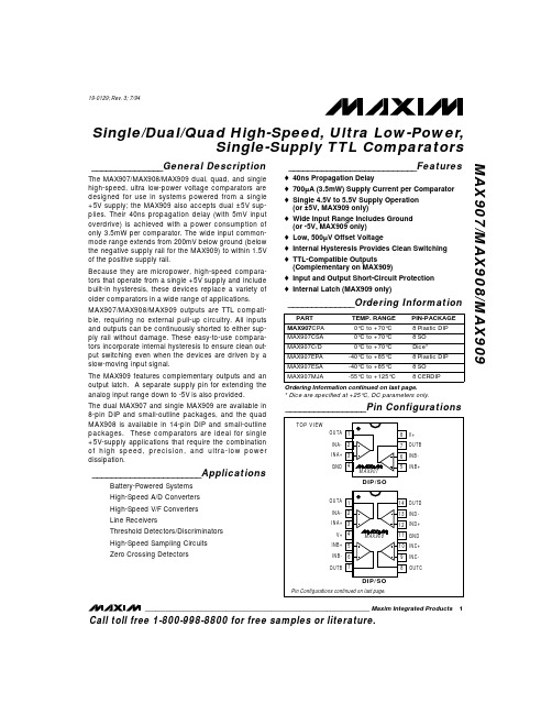
MAX907/MAX908/MAX909
Single/Dual/Quad High-Speed, Ultra Low-Power, Single-Supply TTL Comparators
ABSOLUTE MAXIMUM RATINGS
Positive Supply Voltage (V+ to GND) . . . . . . . . . . . . . . . . . . . . . . . . +7V Negative Supply Voltage (V- to GND, MAX909 only) . . . . . . . . . -7V Differential Input Voltage
High-Speed Sampling Circuits
Zero Crossing Detectors
___________________________Features
o 40ns Propagation Delay o 700µA (3.5mW) Supply Current per Comparator o Single 4.5V to 5.5V Supply Operation
________________________________________________________________ Maxim Integrated Products 1
Call toll free 1-800-998-8800 for free samples or literature.
8 CERDIP
Ordering Information continued on last page. * Dice are specified at +25°C, DC parameters only.
MAX320-MAX322中文资料
ELECTRICAL CHARACTERISTICS
(V+ = +5V ±10%, V- = -5V ±10%, VINH = 3.5V, VINL = 2.5V, TA = TMIN to TMAX, unless otherwise noted.)
PARAMETER ANALOG SWITCH Analog Signal Range
For equivalent devices specified for single-supply operation, see the MAX323/MAX324/MAX325 data sheet. For quad versions of these switches, see the MAX391/MAX392/MAX393 data sheet.
Plastic DIP (derate 9.09mW/°C above +70°C) .............727mW Narrow SO (derate 5.88mW/°C above +70°C) .............471mW
µMAX (derate 4.10mW/°C above +70°C) .....................330mW CERDIP (derate 8.00mW/°C above +70°C) ..................640mW Operating Temperature Ranges MAX32_C_ _ ........................................................0°C to +70°C MAX32_E_ _......................................................-40°C to +85°C MAX32_MJA ...................................................-55°C to +125°C Storage Temperature Range .............................-65°C to +150°C Lead Temperature (soldering, 10sec) .............................+300°C
Fluke199XRAY 医用示波器用户手册说明书

ii
About this Manual
This manual provides information on the X-RAY kVp measurement function of the Fluke 199XRAY Medical ScopeMeter. It also describes user interface differences between the Fluke 190B/C and the Fluke 199XRAY.
Safety Information
Read and comply with the safety instructions that you find in the ScopeMeter 190B/C Series Getting Started manual and in the Fluke 190B/C Users Manual .
®
Fluke199XRAY Medical ScopeMeter
4822 872 30791 August 2006
© 2006 Fluke Corporation, All rights reserved. All product names are trademarks of their respective companies.
1-1
Fluke 199XRAY Users Manual
About the X-RAY kVp Function
The 199XRAY Medical Scopemeter, when used with Fluke Biomedical kVp Divider, automatically measure kVp average and kV peak. In the radiographic measurement mode, exposure time is also measured in milliseconds or pulses.
Maxim美信产品命名规则--赛矽电子何小姐

Maxim产品命名规则第二货源型号命名我们提供的第二货源产品采用特定型号最流行的编号,而不是我们自己的命名规则。
其中包括原有的产品等级、温度范围、封装类型和引脚数编号。
对于第二货源,Maxim经常提供其他厂商不能提供的封装类型和温度范围,这些器件的型号通常采用原来的编码。
自主产品的命名规则绝大多数Maxim产品采用公司专有的命名系统,包括基础型号和后续的3个或4个字母尾缀,有时还带有其它标识符号。
例如:(A)是基础型号基本型号(也称为基础型号)用于区分不同的产品类型,与封装、温度及其它参量无关。
精度等级等参量通常用型号尾缀表示,有些情况下会为不同参量的器件分配一个新的基本型号。
(B)是3字母或4字母尾缀器件具有4个尾缀字母时,第一个尾标代表产品的等级(精度、电压规格、速率等)。
例如:MAX631ACPA中,第一个尾标"A"表示5%的输出精度。
产品数据资料中给出了型号对应的等级。
其余三个字符是3字母尾缀,分别表示温度范围、封装类型和引脚数。
具体含义如下表所示:例如:MAX696CWEC = 工作温度范围为C级(0°C至+70°C)W = 封装类型:W (SOIC 0.300")E = 引脚数,标号为E (这种封装类型为16引脚)请注意:不同的产品类型尾缀代码可能不一致,详细信息或规格说明请参考数据资料。
温度范围商业级 C 0°C至+70°C汽车AEC-Q100 2级 G -40°C 至+105°C汽车AEC-Q100 0级 T -40°C 至+150°C扩展商业级 U 0°C 至+85°C汽车AEC-Q100 1级 A -40°C 至+125°C工业级 I -20°C 至+85°C扩展工业级 E -40°C 至+85°C军品级 M -55°C 至+125°C封装类型A SSOP (缩小外形封装) 209 mil (14, 16, 20, 24, 28引脚);300 mil (36引脚)B UCSP (超小型晶片级封装)C 塑料TO-92;TO-220C LQFP 1.4mm (7mm x 7mm 过孔20mm x 20mm)C TQFP 1.0mm (7mm x 7mm 过孔20mm x 20mm)D 陶瓷Sidebraze 300 mil (8, 14, 16, 18, 20引脚);600 mil (24, 28, 40, 48引脚)E QSOP (四分之一小外型封装)F 陶瓷扁平封装G 金属外壳(金)G QFN (塑料、薄型、四边扁平封装,无引脚冲压) 0.9mmH SBGA (超级球栅阵列θ)H TQFP 1.0mm 5mm x 5mm (32引脚)H TSSOP (薄型缩小外形封装) 4.4mm (8引脚)J CERDIP (陶瓷双列直插) (N) 300 mil (8, 14, 16, 18, 20引脚);(W) 600 mil (24, 28, 40引脚)K SOT 1.23mm (8引脚)L LCC (陶瓷无引线芯片载体) (18, 20, 28引脚)L FCLGA (倒装芯片、基板球栅阵列);薄型LGA (薄型基板球栅阵列) 0.8mm L µDFN (微型双列扁平封装,无引线) (6, 8, 10引脚)M MQFP (公制四边扁平封装)高于1.4mm ;ED-QUAD (28mm x 28mm 160引脚) N PDIP (窄型塑料双列直插封装) 300 mil (24, 28引脚)P PDIP (塑料双列直插封装) 300 mil (8, 14, 16, 18, 20引脚);600 mil (24, 28, 40引脚)Q PLCC (塑料陶瓷无引线芯片载体)R CERDIP (窄型陶瓷双列直插封装) 300 mil (24, 28引脚)S SOIC (窄型塑料小外形封装) 150 milT 金属外壳(镍)T TDFN (塑料、超薄、双列扁平封装,无引线冲压) 0.9mm (6, 8, 10 & 14引脚)T 薄形QFN (塑料、超薄、四列扁平封装,无引线冲压) 0.8mmTQ 薄形QFN (塑料、超薄、四列扁平封装,无引线冲压) 0.8mm (8引脚)U SOT 1.23mm (3, 4, 5, 6引脚)U TSSOP (薄型缩小外形封装) 4.4mm (14, 16, 20, 24, 28, 38, 56引脚);6.1mm (48引脚)U µMAX (薄型缩小外形封装) 3mm x 3mm (8, 10引脚)V U. TQFN (超薄QFN - 塑装、超薄四边扁平,无引线冲压) 0.55mm W SOIC (宽型、塑料小外形封装) 300 milW WLP (晶片级封装)X CSBGA 1.4mmX CVBGA 1.0mmX SC70Y SIDEBRAZE (窄型) 300 mil (24, 28引脚),超薄LGA 0.5mmZ 薄型SOT 1mm (5, 6, 8引脚)引脚数A 8, 25, 46, 182B 10, 64C 12, 192D 14, 128E 16, 144F 22, 256G 24, 81H 44, 126I 28, 57J 32, 49K 5, 68, 265L 9, 40M 7, 48, 267N 18, 56O 42, 73P 20, 96Q 2, 100R 3, 84S 4, 80T 6, 160U 38, 60V 8 (.200"引脚圆周,隔离外壳), 30, 196W 10 (.230"引脚圆周,隔离外壳), 169X 36, 45Y 8 (.200"引脚圆周,外壳接引脚4), 52Z 10 (.230"引脚圆周,外壳接引脚5), 26, 72(C)其它尾缀字符在3字母或4字母尾缀的后面可能还会出现其它字符,这些字符可能单独出现,也可能与型号组合在一起。
LM199中文资料

LM199/LM299/LM399/LM3999Precision ReferenceGeneral DescriptionThe LM199series are precision,temperature-stabilized monolithic zeners offering temperature coefficients a factor of ten better than high quality reference zeners.Constructed on a single monolithic chip is a temperature stabilizer circuit and an active reference zener.The active circuitry reduces the dynamic impedance of the zener to about 0.5Ωand al-lows the zener to operate over 0.5mA to 10mA current range with essentially no change in voltage or temperature coefficient.Further,a new subsurface zener structure gives low noise and excellent long term stability compared to ordi-nary monolithic zeners.The package is supplied with a ther-mal shield to minimize heater power and improve tempera-ture regulation.The LM199series references are exceptionally easy to use and free of the problems that are often experienced with or-dinary zeners.There is virtually no hysteresis in reference voltage with temperature cycling.Also,the LM199is free of voltage shifts due to stress on the leads.Finally,since the unit is temperature stabilized,warm up time is fast.The LM199can be used in almost any application in place of ordinary zeners with improved performance.Some ideal ap-plications are analog to digital converters,calibration stan-dards,precision voltage or current sources or precision power supplies.Further in many cases the LM199can re-place references in existing equipment with a minimum of wiring changes.The LM199series devices are packaged in a standard her-metic TO-46package inside a thermal shield.The LM199is rated for operation from −55˚C to +125˚C while the LM299is rated for operation from −25˚C to +85˚C and the LM399is rated from 0˚C to +70˚C.The LM3999is packaged in a standard TO-92package and is rated from 0˚C to +70˚CFeaturesn Guaranteed 0.0001%/˚C temperature coefficient n Low dynamic impedance —0.5Ωn Initial tolerance on breakdown voltage —2%n Sharp breakdown at 400µAn Wide operating current —500µA to 10mA n Wide supply range for temperature stabilizer n Guaranteed low noisen Low power for stabilization —300mW at 25˚C n Long term stability —20ppmnProven reliability,low-stress packaging in TO-46integrated-circuit hermetic package,for low hysteresis after thermal cycling.33million hours MTBF at T A =+25˚C (T J =+86˚C)n Certified long term stability available n MIL-STD-883compliantConnection DiagramsMetal Can Package (TO-46)DS005717-14Top ViewLM199/LM299/LM399(See Table on fourth page)NS Package Number H04DPlastic Package TO-92DS005717-10Bottom ViewLM3999(See Table on fourth page)NS Package Number Z03AMay 1999LM199/LM299/LM399/LM3999Precision Reference©1999National Semiconductor Corporation Functional Block DiagramsLM199/LM299/LM399DS005717-15LM3999 2Absolute Maximum Ratings(Note1) Specifications for Military/Aerospace products are not contained in this datasheet.Refer to the following Reli-ability Electrical Test Specifications documents: RETS199X for LM199,RETS199AX for LM199A. Temperature Stabilizer VoltageLM199/LM299/LM39940V LM399936V Reverse Breakdown Current20mA Forward CurrentLM199/LM299/LM3991mA LM3999−0.1mA Reference to Substrate Voltage V(RS)(Note2)40V−0.1V Operating Temperature RangeLM199−55˚C to+125˚C LM299−25˚C to+85˚C LM399/LM3999−0˚C to+70˚C Storage Temperature Range−55˚C to+150˚C Soldering InformationTO-92package(10sec.)+260˚C TO-46package(10sec.)+300˚CElectrical Characteristics(Notes3,6)Parameter Conditions LM199H/LM299H LM399H UnitsMin Typ Max Min Typ Max Reverse Breakdown Voltage0.5mA≤I R≤10mA 6.8 6.957.1 6.6 6.957.3V Reverse Breakdown Voltage0.5mA≤I R≤10mA69612mV Change with CurrentReverse Dynamic Impedance I R=1mA0.510.5 1.5ΩReverse Breakdown−55˚C≤T A≤+85˚CLM1990.000030.0001%/˚CTemperature Coefficient+85˚C≤T A≤+125˚C0.00050.0015%/˚C−25˚C≤T A≤85˚C LM2990.000030.0001%/˚C0˚C≤T A≤+70˚C LM3990.000030.0002%/˚C RMS Noise10Hz≤f≤10kHz720750µV Long Term Stability Stabilized,22˚C≤T A≤28˚C,2020ppm1000Hours,I R=1mA±0.1%Temperature Stabilizer T A=25˚C,Still Air,V S=30V8.5148.515mA Supply Current T A=−55˚C2228Temperature Stabilizer940940V Supply VoltageWarm-Up Time to0.05%V S=30V,T A=25˚C33sec. Initial Turn-on Current9≤V S≤40,T A=+25˚C,(Note4)140200140200mA Note1:“Absolute Maximum Ratings”indicate limits beyond which damage to the device may occur.Operating Ratings indicate conditions for which the device is functional,but do not guarantee specific performance limits.Electrical Characteristics(Note3)Parameter Conditions LM3999Z UnitsMin Typ MaxReverse Breakdown Voltage0.6mA≤I R≤10mA 6.6 6.957.3V Reverse Breakdown Voltage0.6mA≤I R≤10mA620mV Change with CurrentReverse Dynamic Impedance I R=1mA0.6 2.2ΩReverse Breakdown0˚C≤T A≤70˚C0.00020.0005%/˚C Temperature CoefficientRMS Noise10Hz≤f≤10kHz7µV Long Term Stability Stabilized,22˚C≤T A≤28˚C,20ppm1000Hours,I R=1mA±0.1%Temperature Stabilizer T A=25˚C,Still Air,V S=30V1218mA Temperature Stabilizer36V Supply VoltageWarm-Up Time to0.05%V S=30V,T A=25˚C5sec.3Electrical Characteristics(Note3)(Continued)Parameter Conditions LM3999Z UnitsMin Typ MaxInitial Turn-On Current9≤V S≤40,T A=25˚C140200mAElectrical Characteristics(Notes3,6)Parameter Conditions LM199AH,LM299AH LM399AH UnitsMin Typ Max Min Typ Max Reverse Breakdown Voltage0.5mA≤I R≤10mA 6.8 6.957.1 6.6 6.957.3V Reverse Breakdown Voltage0.5mA≤I R≤10mA69612mV Change with CurrentReverse Dynamic Impedance I R=1mA0.510.5 1.5ΩReverse Breakdown−55˚C≤T A≤+85˚CLM199A 0.000020.00005%/˚CTemperature Coefficient+85˚C≤T A≤+125˚C0.00050.0010%/˚C−25˚C≤T A≤85˚C LM299A0.000020.00005%/˚C0˚C≤T A≤+70˚C LM399A0.000030.0001%/˚C RMS Noise10Hz≤f≤10kHz720750µV Long Term Stability Stabilized,22˚C≤T A≤28˚C,2020ppm1000Hours,I R=1mA±0.1%Temperature Stabilizer T A=25˚C,Still Air,V S=30V8.5148.515mA Supply Current T A=−55˚C2228Temperature Stabilizer940940V Supply VoltageWarm-Up Time to0.05%V S=30V,T A=25˚C33sec. Initial Turn-on Current9≤V S≤40,T A=+25˚C,(Note4)140200140200mA Note2:The substrate is electrically connected to the negative terminal of the temperature stabilizer.The voltage that can be applied to either terminal of the refer-ence is40V more positive or0.1V more negative than the substrate.Note3:These specifications apply for30V applied to the temperature stabilizer and−55˚C≤T A≤+125˚C for the LM199;−25˚C≤T A≤+85˚C for the LM299and 0˚C≤T A≤+70˚C for the LM399and LM3999.Note4:This initial current can be reduced by adding an appropriate resistor and capacitor to the heater circuit.See the performance characteristic graphs to de-termine values.Note5:Do not wash the LM199with its polysulfone thermal shield in TCE.Note6:A military RETS electrical test specification is available for the LM199H/883,LM199AH/883,and LM199AH-20/883on request.Ordering InformationInitial0˚C to+70˚C−25˚C to+85˚C−55˚C to+125˚C NS Tolerance Package 2%LM299AH LM199AH,LM199AH/883H04D5%LM399H LM299H H04D LM399AH5%LM3999Z Z03ACertified Long Term DriftThe National Semiconductor LM199AH-20,LM299AH-20, and LM399AH-50are ultra-stable Zener references specially selected from the production runs of LM199AH,LM299AH, LM399AH and tested to confirm a long-term stability of20, 20,or50ppm per1000hours,respectively.The devices are measured every168hours and the voltage of each device is logged and compared in such a way as to show the deviation from its initial value.Each measurement is taken with a probable-worst-case deviation of±2ppm,compared to the Reference Voltage,which is derived from several groups of NBS-traceable references such as LM199AH-20’s,1N827’s,and saturated standard cells,so that the deviation of any one group will not cause false indications.Indeed,this compari-son process has recently been automated using a specially prepared computer program which is custom-designed to re-ject noisy data(and require a repeat reading)and to record the average of the best5of7readings,just as a sagacious standards engineer will reject unbelievable readings.The typical characteristic for the LM199AH-20is shown be-low.This computerized print-out form of each reference’s stability is shipped with the unit.4Typical CharacteristicsNational SemiconductorCertified Long Term DriftHrs Drift168−20336−24504−36672−34840−401008−36Testing ConditionsHeater Voltage:30VZener Current:1mAAmbient Temp.:25˚CTypical Performance CharacteristicsDS005717-12Reverse CharacteristicsDS005717-19Reverse Voltage ChangeDS005717-20Dynamic ImpedanceDS005717-21Zener Noise VoltageDS005717-22Stabilization TimeDS005717-23Heater CurrentDS005717-24 5Typical Performance Characteristics(Continued)Typical ApplicationsInitial Heater CurrentDS005717-25Heater Current(To Limit ThisSurge,See Next Graph)DS005717-26Heater Surge Limit Resistor vsMinimum Supply Voltage at VariousMinimum TemperaturesDS005717-27*Heater must be bypassed with a2µF or largertantalum capacitor if resistors are used.Low Frequency Noise VoltageDS005717-3Response TimeDS005717-7Single Supply OperationDS005717-28Split Supply OperationDS005717-296Typical Applications(Continued)Negative Heater Supply with Positive ReferenceDS005717-30Buffered ReferenceWith Single SypplyDS005717-31Positive Current SourceDS005717-32Standard Cell ReplacementDS005717-33 7Typical Applications(Continued)Negative Current SourceDS005717-34Square Wave Voltage Reference DS005717-35Portable Calibrator*DS005717-36*Warm-up time 10seconds;intermittent operation does not degrade long term stability.14V Reference DS005717-37Precision Clamp*DS005717-38*Clamp will sink 5mA when input goes more positive than reference 8Typical Applications(Continued)0V to20V Power ReferenceDS005717-39Bipolar Output ReferenceDS005717-40Voltage ReferenceDS005717-99Schematic DiagramsTemperature StabilizerDS005717-1ReferenceDS005717-13 10Physical Dimensions inches(millimeters)unless otherwise notedOrder Number LM299H,LM399H,LM199AH,LM199AH/883LM299AH or LM399AHNS Package H04DPlastic PackageOrder Number LM3999ZNS Package Z03A11NotesLIFE SUPPORT POLICYNATIONAL’S PRODUCTS ARE NOT AUTHORIZED FOR USE AS CRITICAL COMPONENTS IN LIFE SUPPORT DEVICES OR SYSTEMS WITHOUT THE EXPRESS WRITTEN APPROVAL OF THE PRESIDENT AND GENERAL COUNSEL OF NATIONAL SEMICONDUCTOR CORPORATION.As used herein:1.Life support devices or systems are devices or systems which,(a)are intended for surgical implant into the body,or (b)support or sustain life,and whose failure to perform when properly used in accordance with instructions for use provided in the labeling,can be reasonably expected to result in a significant injury to the user.2.A critical component is any component of a life support device or system whose failure to perform can be reasonably expected to cause the failure of the life support device or system,or to affect its safety or effectiveness.National Semiconductor Corporation AmericasTel:1-800-272-9959Fax:1-800-737-7018Email:support@National Semiconductor EuropeFax:+49(0)180-5308586Email:europe.support@Deutsch Tel:+49(0)180-5308585English Tel:+49(0)180-5327832Français Tel:+49(0)180-5329358Italiano Tel:+49(0)180-5341680National Semiconductor Asia Pacific Customer Response Group Tel:65-2544466Fax:65-2504466Email:sea.support@National Semiconductor Japan Ltd.Tel:81-3-5639-7560Fax:81-3-5639-7507L M 199/L M 299/L M 399/L M 3999P r e c i s i o n R e f e r e n c eNational does not assume any responsibility for use of any circuitry described,no circuit patent licenses are implied and National reserves the right at any time without notice to change said circuitry and specifications.。
BAV199中文资料

BAV199中文资料DATA SHEETProduct speci?cationSupersedes data of 1996Mar 131999May 11DISCRETE SEMICONDUCTORSBAV199Low-leakage double diodeook, halfpageM3D088Low-leakage double diodeBAV199FEATURESPlastic SMD packageLow leakage current: typ. 3pA ?Switching time: typ.0.8μs ?Continuous reverse voltage:max.75VRepetitive peak reverse voltage:max.85VRepetitive peak forward current:max. 500mA.APPLICATION Low-leakage current applications in surface mounted circuits.DESCRIPTIONEpitaxial, medium-speed switching,double diode in a small SOT23 plastic SMD package. The diodes are connected in series.PINNINGPIN DESCRIPTION1anode 2cathode 3anode; cathodeFig.1 Simplified outline (SOT23) and symbol.Marking code: JYp =made in Hong Kong; JYt =made in Malaysia.handbook, 4 columns213Top viewMAM107213LIMITING VALUESIn accordance with the Absolute Maximum Rating System (IEC 134).Note1.Device mounted on a FR4 printed-circuit board.SYMBOL PARAMETERCONDITIONSMIN.MAX.UNITPer diode V RRM repetitive peak reverse voltage ?85V V R continuous reverse voltage ?75V I F continuous forward current single diode loaded; note 1; see Fig.2?160mA double diode loaded; note 1; see Fig.2140mA I FRM repetitive peak forward current ?500mAI FSMnon-repetitive peak forward currentsquare wave; T j =25°C prior to surge;see Fig.4t p =1μs ?4A t p =1ms ?1A t p =1s0.5A P tot total power dissipation T amb =25°C; note 1250mW T stg storage temperature ?65+150°C T j junctiontemperature150°CLow-leakage double diodeBAV199ELECTRICAL CHARACTERISTICS T j =25°C unless otherwise speci?ed.THERMAL CHARACTERISTICS Note1.Device mounted on a FR4 printed-circuit board.SYMBOL PARAMETERCONDITIONSTYP .MAX.UNITPer diode V Fforward voltagesee Fig.3I F =1mA ?900mV I F =10mA ?1000mV I F =50mA ?1100mV I F =150mA1250mV I Rreverse currentsee Fig.5V R =75V0.0035nA V R =75V; T j =150°C380nA C d diode capacitance f =1MHz; V R =0; see Fig.62?pF t rrreverse recovery timewhen switched from I F =10mA to I R =10mA; R L =100?;measured at I R =1mA; see Fig.70.83μsSYMBOL PARAMETERCONDITIONSVALUE UNIT R th j-tp thermal resistance from junction to tie-point 360K/W R th j-a thermal resistance from junction to ambientnote 1500K/WLow-leakage double diodeBAV199GRAPHICAL DATADevice mounted on a FR4 printed-circuit board.Fig.2Maximum permissible continuous forwardcurrent as a function of ambient temperature.handbook, halfpage0200300100200MLB756100T ( C)amboI F (mA)single diode loadeddouble diode loadedFig.3Forward current as a function of forward voltage; per diode.handbook, halfpage0 1.6300100200MLB752 - 10.8 1.20.4I F (mA)V (V)F(1)(2)(3)(1)T j =150°C; typical values.(2)T j =25°C; typical values.(3)T j =25°C; maximum values.Fig.4 Maximum permissible non-repetitive peak forward current as a function of pulse duration per diode.Based on square wave currents; T j =25°C prior to surge.handbook, full pagewidthMBG70410t p (μs)1I FSM (A)10210?1104102103101Low-leakage double diode BAV199V R =75V.(1)Maximum values.(2)Typical values.Fig.5Reverse current as a function of junction temperature; per diode.handbook, halfpage102103150200500MLB754100101101102I R (nA)T ( C)oj(1)(2)Fig.6Diode capacitance as a function of reverse voltage; per diode; typical values.f =1MHz; T j =25°C.handbook, halfpage0102015521MBG526V R (V)C d(pF)handbook, full pagewidtht rr(1)I F toutput signalt rtt p10%90%V Rinput signal V = V I x R R F SR = 50SI FD.U.T.R = 50iSAMPLING OSCILLOSCOPEMGA881Fig.7 Reverse recovery time test circuit and waveforms. Low-leakage double diodeBAV199PACKAGE OUTLINEUNIT A 1max.b p c D E e 1H E L p Q w v REFERENCES OUTLINE VERSION EUROPEAN PROJECTIONISSUE DATE 97-02-28IECJEDECEIAJmm0.10.480.380.150.093.02.81.41.20.95e 1.92.52.10.550.450.10.2DIMENSIONS (mm are the original dimensions)0.450.15 SOT23b pD e 1eAA 1L pQdetail XH EE w M v M ABAB 01 2 mmscaleA 1.10.9cX123Plastic surface mounted package; 3 leadsSOT23Low-leakage double diode BAV199DEFINITIONSData Sheet StatusObjective speci?cation This data sheet contains target or goal speci?cations for product development. Preliminary speci?cation This data sheet contains preliminary data; supplementary data may be published later. Product speci?cation This data sheet contains ?nal product speci?cations.Limiting valuesLimiting values given are in accordance with the Absolute Maximum Rating System (IEC 134). Stress above one or more of the limiting values may cause permanent damage to the device. These are stress ratings only and operation of the device at these or at any other conditions above those given in the Characteristics sections of the speci?cation is not implied. Exposure to limiting values for extended periods may affect device reliability.Application informationWhere application information is given, it is advisory and does not form part of the speci?cation.LIFE SUPPORT APPLICATIONSThese products are not designed for use in life support appliances, devices, or systems where malfunction of these products can reasonably be expected to result in personal injury. Philips customers using or selling these products for use in such applications do so at their own risk and agree to fully indemnifyPhilips for any damages resulting from such improper use or sale.Philips Electronics N.V. SCA All rights are reserved. Reproduction in whole or in part is prohibited without the prior written consent of the copyright owner.The information presented in this document does not form part of any quotation or contract, is believed to be accurate and reliable and may be changed without notice. No liability will be accepted by the publisher for any consequence of its use. Publication thereof does not convey nor imply any license under patent- or other industrial or intellectual property rights.Internet: /doc/8616113895.html,199964Philips Semiconductors – a worldwide companyNetherlands: Postbus 90050, 5600PB EINDHOVEN, Bldg.VB,Tel.+31402782785,Fax.+31402788399New Zealand: 2Wagener Place, C.P.O.Box 1041, AUCKLAND,Tel.+6498494160,Fax.+6498497811Norway: Box 1, Manglerud 0612, OSLO,Tel.+4722748000,Fax.+4722748341Pakistan: see Singapore Philippines: Philips Semiconductors Philippines Inc.,106Valero St.Salcedo Village, P.O.Box 2108MCC,MAKATI,Metro MANILA, Tel.+6328166380,Fax.+6328173474Poland: Ul.Lukiska 10, PL 04-123WARSZAWA,Tel.+48226122831,Fax.+48226122327Portugal: see Spain Romania: see ItalyRussia: Philips Russia, /doc/8616113895.html,atcheva 35A, 119048MOSCOW,T el.+70957556918,Fax.+70957556919 Singapore: Lorong 1, Toa Payoh, SINGAPORE319762,Tel.+653502538,Fax.+652516500Slovakia: see Austria Slovenia: see ItalySouth Africa: S.A. PHILIPS Pty Ltd., 195-215Main Road Martindale,2092JOHANNESBURG, P.O.Box 58088 Newville 2114,Tel.+27114715401,Fax.+27114715398South America: Al.Vicente Pinzon,173, 6th floor,04547-130S?O PAULO,SP, Brazil,Tel.+55118212333,Fax.+55118212382Spain: Balmes 22, 08007BARCELONA,Tel.+34933016312,Fax.+34933014107 Sweden: Kottbygatan 7, Akalla, S-16485STOCKHOLM,Tel.+46859852000,Fax.+46859852745 Switzerland: Allmendstrasse 140, CH-8027ZüRICH,Tel.+4114882741Fax.+4114883263Taiwan: Philips Semiconductors, 6F, No.96, Chien Kuo N.Rd.,Sec.1,TAIPEI, Taiwan Tel.+886221342886,Fax.+886221342874Thailand: PHILIPS ELECTRONICS (THAILAND) Ltd.,209/2Sanpavuth-Bangna Road Prakanong, BANGKOK 10260,Tel.+6627454090,Fax.+6623980793Turkey: Yukari Dudullu, Org. San. Blg., 2.Cad. Nr. 28 81260Umraniye,ISTANBUL,Tel.+902165221500,Fax.+902165221813Ukraine : PHILIPS UKRAINE, 4Patrice Lumumba str., Building B, Floor 7,252042KIEV, Tel.+380442642776, Fax. +380442680461 United Kingdom: Philips Semiconductors Ltd., 276Bath Road, Hayes,MIDDLESEX UB35BX, Tel.+441817305000,Fax.+441817548421United States: 811East Arques Avenue, SUNNYVALE, CA 94088-3409,Tel.+18002347381, Fax.+18009430087Uruguay: see South America Vietnam: see SingaporeYugoslavia: PHILIPS, Trg N. Pasica 5/v, 11000BEOGRAD,Tel.+38111625344,Fax.+38111635777 For all other countries apply to: Philips Semiconductors,International Marketing &Sales Communications, Building BE-p, P.O.Box 218,5600MD EINDHOVEN, The Netherlands,Fax.+31402724825Argentina: see South America Australia: 34 Waterloo Road, NORTH RYDE, NSW 2113,Tel.+61298054455,Fax.+61298054466Austria:Computerstr. 6, A-1101 WIEN, P.O. Box 213,Tel.+431601011248, Fax.+431601011210Belarus: Hotel Minsk Business Center, Bld.3, r.1211, Volodarski Str.6,220050MINSK, Tel.+375172200733,Fax.+375172200773Belgium: see The Netherlands Brazil:see South AmericaBulgaria:Philips Bulgaria Ltd., Energoproject, 15th floor,51James Bourchier Blvd., 1407SOFIA,T el.+3592689211,Fax.+3592689102Canada: PHILIPS SEMICONDUCTORS/COMPONENTS,T el.+18002347381,Fax.+18009430087China/Hong Kong: 501Hong Kong Industrial Technology Centre,72Tat Chee Avenue, Kowloon Tong, HONG KONG,Tel.+852********,Fax.+852********Colombia: see South America Czech Republic: see AustriaDenmark: Sydhavnsgade 23, 1780COPENHAGEN V,Tel.+4533293333,Fax.+4533293905Finland: Sinikalliontie 3, FIN-02630ESPOO,T el.+3589615800,Fax.+358961580920 France: 51Rue Carnot, BP317, 92156SURESNES Cedex,Tel.+33140996161,Fax.+33140996427Germany: Hammerbrookstra?e 69, D-20097HAMBURG,T el.+4940235360,Fax.+494023536300Hungary: see AustriaIndia: Philips INDIA Ltd, Band Box Building, 2nd floor,254-D,Dr.Annie Besant Road, Worli, MUMBAI 400025,Tel.+91224938541,Fax.+91224930966Indonesia: PT Philips Development Corporation, Semiconductors Division,Gedung Philips, Jl. Buncit Raya Kav.99-100, JAKARTA 12510,Tel.+62217940040ext.2501, Fax.+62217940080Ireland: Newstead, Clonskeagh, DUBLIN 14,Tel.+35317640000,Fax.+35317640200Israel: RAPAC Electronics, 7Kehilat Saloniki St, PO Box 18053,TEL AVIV 61180, Tel.+97236450444,Fax.+97236491007Italy: PHILIPS SEMICONDUCTORS, Piazza IV Novembre 3,20124MILANO, Tel.+390267522531,Fax.+390267522557Japan: Philips Bldg 13-37, Kohnan 2-chome, Minato-ku,TOKYO 108-8507, Tel.+81337405130,Fax.+81337405077Korea: Philips House, 260-199Itaewon-dong, Yongsan-ku, SEOUL,Tel.+8227091412,Fax.+8227091415Malaysia: No.76Jalan Universiti, 46200PETALING JAYA, SELANGOR,Tel.+60 37505214,Fax.+6037574880Mexico: 5900Gateway East, Suite 200, EL PASO, TEXAS 79905,Tel.+9-58002347381, Fax +9-58009430087Middle East: see ItalyPrinted in The Netherlands115002/00/03/pp8 Date of release: 1999May 11Document order number: 939775005946。
- 1、下载文档前请自行甄别文档内容的完整性,平台不提供额外的编辑、内容补充、找答案等附加服务。
- 2、"仅部分预览"的文档,不可在线预览部分如存在完整性等问题,可反馈申请退款(可完整预览的文档不适用该条件!)。
- 3、如文档侵犯您的权益,请联系客服反馈,我们会尽快为您处理(人工客服工作时间:9:00-18:30)。
19-0401; Rev 0; 6/95
Multi-Range (±4V, ±2V, +4V, +2V), +5V Supply, 12-Bit DAS with 8+4 Bus Interface
_______________General Description
Stresses beyond those listed under “Absolute Maximum Ratings” may cause permanent damage to the device. These are stress ratings only, and functional operation of the device at these or any other conditions beyond those indicated in the operational sections of the specifications is not implied. Exposure to absolute maximum rating conditions for extended periods may affect device reliability.
MAX199
______________Ordering Information
PART MAX199ACNI TEMP. RANGE 0°C to +70°C PIN-PACKAGE 28 Narrow Plastic DIP
MAX199BCNI 0°C to +70°C 28 Narrow Plastic DIP MAX199ACWI 0°C to +70°C 28 Wide SO MAX199BCWI 0°C to +70°C 28 Wide SO MAX199ACAI 0°C to +70°C 28 SSOP MAX199BCAI 0°C to +70°C 28 SSOP MAX199BC/D 0°C to +70°C Dice* Ordering Information continued at end of data sheet. *Dice are specified at TA = +25°C, DC parameters only.
RD 4 HBEN 5 SHDN 6 D7 7 D6 8 D5 9 D4 10 D3/D11 11 D2/D10 12 D1/D9 13 D0/D8 14
MAX199
24 INT 23 CH7 22 CH6 21 CH5 20 CH4 19 CH3 18 CH2 17 CH1 16 CH0 15 AGND
The MAX199 multi-range, 12-bit data-acquisition system (DAS) requires only a single +5V supply for operation, and converts analog signals up to ±4V at its inputs. This system provides eight analog input channels that are independently software programmable for a variety of ranges: ±VREF, ±VREF/2, 0V to VREF, or 0V to VREF/2. This increases effective dynamic range to 14 bits, and provides the user flexibility to interface 4mA-to-20mA, ±12V, and ±15V powered sensors to a single +5V system. In addition, the converter is fault-protected to ±16.5V; a fault condition on any channel will not affect the conversion result of the selected channel. Other features include a 5MHz bandwidth track/hold, 100ksps throughput rate, internal/external clock, internal/external acquisition control, 8+4 parallel interface, and operation with an internal 4.096V or external reference. A hardware SHDN pin and two programmable powerdown modes (STBYPD, FULLPD) provide low-current shutdown between conversions. In STBYPD mode, the reference buffer remains active, eliminating start-up delays. The MAX199 employs a standard microprocessor (µP) interface. Its three-state data I/O interface is configured to operate with 8-bit data buses, and data-access and bus-release timing specifications are compatible with most popular µPs. All logic inputs and outputs are TTL/CMOS compatible. The MAX199 is available in 28-pin DIP, wide SO, SSOP, and ceramic SB packages. For a different combination of input ranges (±10V, ±5V, 0V to 10V, 0V to 5V), see the MAX197 data sheet. For 12bit bus interfaces, see the MAX196/MAX198 data sheet.
Call toll free 1-800-722-8266 for free samples or literature.
元器件交易网
Multi-Range (±4V, ±2V, +4V, +2V), +5V Supply, 12-Bit DAS with 8+4 Bus Interface MAX199
Functional Diagram appears at end of data sheet.
DIP/SO/SSOP/Ceramic SB 1
________________________________________________________________ Maxim Integrated Products
ABSOLUTE MAXIMUM RATINGS
VDD to AGND............................................................-0.3V to +7V AGND to DGND.....................................................-0.3V to +0.3V REF to AGND..............................................-0.3V to (VDD + 0.3V) REFADJ to AGND.......................................-0.3V to (VDD + 0.3V) Digital Inputs to DGND...............................-0.3V to (VDD + 0.3V) Digital Outputs to DGND ............................-0.3V to (VDD + 0.3V) CH0–CH7 to AGND ..........................................................±16.5V Continuous Power Dissipation (TA = +70°C) Narrow Plastic DIP (derate 14.29mW/°C above +70°C)....1143mW Wide SO (derate 12.50mW/°C above +70°C)..............1000mW SSOP (derate 9.52mW/°C above +70°C) ......................762mW Narrow Ceramic SB (derate 20.00mW/°C above +70°C)..1600mW Operating Temperature Ranges MAX199_C_ _ .......................................................0°C to +70°C MAX199_E_ _.....................................................-40°C to +85°C MAX199_M_ _ ..................................................-55°C to +125°C Storage Temperature Range .............................-65°C to +150°C Lead Temperature (soldering, 10sec) .............................+300°C