IT3D2-180S-BGA(57);中文规格书,Datasheet资料
1SS383T1G;中文规格书,Datasheet资料

© Semiconductor Components Industries, LLC, 2006 March, 2006 − Rev. 21Publication Order Number:1SS383T1G/D1SS383T1GPreferred DeviceDual Schottky DiodeDual 40 V, 300 mA Low V F Schottky Diodes in 4−lead SC−82 package.Features•Low Forward V oltage: V F = 0.48 V (typ) @ I F = 100 mA •Low Reverse Current: I R = 5 m A (max)•This is a Pb−Free Device*MAXIMUM RATINGS (T A = 25°C)Rating Symbol Max Unit Continuous Reverse Voltage V R40V Maximum Peak Forward Current*I FM300mA Peak Forward Surge CurrentPulse Width = 10 m sI FM(surge)500mA THERMAL CHARACTERISTICSCharacteristic(Both Junctions Heated)Symbol Max UnitTotal Device Dissipation T A = 25°CDerate above 25°C P D200(Note 1)1.6(Note 1)mWmW/°CThermal Resistance, Junction-to-Ambient R q JA625(Note 1)°C/WJunction and StorageTemperatureT J, T stg−55 to +150°CStresses exceeding Maximum Ratings may damage the device. Maximum Ratings are stress ratings only. Functional operation above the Recommended Operating Conditions is not implied. Extended exposure to stresses above the Recommended Operating Conditions may affect device reliability.*Both Devices Active1.FR−4 @ Minimum Pad.ELECTRICAL CHARACTERISTICS (T A = 25°C unless otherwise noted) Characteristic SymbolMin Typ Max UnitForward Voltage (I F = 1.0 mA) (I F = 10 mA) (I F = 100 mA)V F−−−280360540−−600mVReverse Current (V R = 40 V)IR−−5m ACapacitance(V R = 0, f = 1.0 MHz)C D−−25pF*For additional information on our Pb−Free strategy and soldering details, please download the ON Semiconductor Soldering and Mounting Techniques Reference Manual, SOLDERRM/D.Preferred devices are recommended choices for future use and best overall value.21Device Package Shipping†ORDERING INFORMATION1SS383T1G SC−82(Pb−Free)3000/T ape & Reel34†For information on tape and reel specifications, including part orientation and tape sizes, please refer to our Tape and Reel Packaging Specification Brochure, BRD8011/D.1SS383T1GPACKAGE DIMENSIONSSC−82, 4 LEAD, GULL WINGCASE 900AA−01ISSUE ONOTES:1.DIMENSIONING AND TOLERANCING PER ANSI Y14.5M, 1982.2.CONTROLLING DIMENSION: MILLIMETERS3.MAXIMUM LEAD THICKNESS INCLUDES LEADFINISH THICKNESS. MINIMUM LEAD THICKNESS IS THE MINIMUMTHICKNESS OF BASE MATERIAL.4.DIMENSIONS A AND B DO NOT INCLUDE MOLD FLASH, PROTRUSIONS, OR GATE BURRS.STYLE 1:PIN 1.ANODE 12.ANODE 23.CATHODE 24.CATHODE 1DIM MIN NOM MAX MILLIMETERS A 0.800.90 1.00A 0−−−0.10b 0.100.200.30C 0.100.180.25D 1.80 2.00 2.20E 1.15 1.25 1.35e 1.30 BSC 2.00 2.10 2.20L0.100.200.300.0320.0350.040−−−0.0040.0040.0080.0120.0040.0070.0100.0710.0790.0870.0450.0490.0530.051 BSC 0.0790.0830.0870.0040.0080.012MIN NOM MAX INCHES1H E ON Semiconductor and are registered trademarks of Semiconductor Components Industries, LLC (SCILLC). SCILLC reserves the right to make changes without further notice to any products herein. SCILLC makes no warranty, representation or guarantee regarding the suitability of its products for any particular purpose, nor does SCILLC assume any liability arising out of the application or use of any product or circuit, and specifically disclaims any and all liability, including without limitation special, consequential or incidental damages.“Typical” parameters which may be provided in SCILLC data sheets and/or specifications can and do vary in different applications and actual performance may vary over time. All operating parameters, including “Typicals” must be validated for each customer application by customer’s technical experts. SCILLC does not convey any license under its patent rights nor the rights of others. SCILLC products are not designed, intended, or authorized for use as components in systems intended for surgical implant into the body, or other applications intended to support or sustain life, or for any other application in which the failure of the SCILLC product could create a situation where personal injury or death may occur. Should Buyer purchase or use SCILLC products for any such unintended or unauthorized application, Buyer shall indemnify and hold SCILLC and its officers, employees, subsidiaries, affiliates,and distributors harmless against all claims, costs, damages, and expenses, and reasonable attorney fees arising out of, directly or indirectly, any claim of personal injury or death associated with such unintended or unauthorized use, even if such claim alleges that SCILLC was negligent regarding the design or manufacture of the part. SCILLC is an Equal Opportunity/Affirmative Action Employer. This literature is subject to all applicable copyright laws and is not for resale in any manner.PUBLICATION ORDERING INFORMATION分销商库存信息: ONSEMI1SS383T1G。
S1800资料

Applications & Features
• Sub-miniature, 1.1 mm high ceramic package ideal for SMT applications
• 10µA max standby mode on S1800 and S1803
• Available as 3.3V and 5V versions • CMOS, HCMOS & TTL compatible • Perfect for PC's; notebook, palmtop
SaRonix
Crystal Clock Oscillator
3.3 & 5V, HCMOS, TTL, SMD S1800 / S1803 / S1850 Series
Tri-State Logic Table
Pad 1 Input
Pad 3 Output
Logic 1 or NC
Oscillation
元器件交易网
Technical Data
SaRonix
Crystal Clock Oscillator
3.3 & 5V, HCMOS, TTL, SMD S1800 / S1803 / S1850 Series
ACTUAL SIZE
Description
The 5V S1800, S1850 and 3.3V S1803 are crystal-controlled, low-current oscillators providing precise rise and fall times to drive high speed CMOS and TTL loads. The sub-miniature, very low profile leadless ceramic packages have gold-plated contact pads, ideal for today's pick-and-place SMT environments. The S1850 is a high output load version available to 80 MHz.
SI2302-TP;中文规格书,Datasheet资料

Revision: A
/
3 of 5
2011/01/01
VGS, Gate to Source Voltage (V) ID, Drain Current (A)
VTH, Normalized Gate-Source Threshold Voltage
RDS(ON), Normalized RDS(ON), On-Resistance(Ohms)
IS, Source-drain current (A)
ID, Drain Current (A)
SI2302
10 25 C
Maximum Ratings @ 25OC Unless Otherwise Specified
Symbol VDS ID IDM VGS
PD R©JA
TJ
TSTG
Parameter Drain-source Voltage Drain Current-Continuous Drain Current-Pulsed a Gate-source Voltage
MCC
TM
Micro Commercial Components
5 VDS=10V ID=3.6A
4
3
2
1
0
0
2
4
6
Qg, Total Gate Charge (nC)
Figure 7. Gate Charge
VDD
RL VIN
D
VOUT
VGS
RGEN G
S
Figure 9. Switching Test Circuit
CG2145MS,CG2800MS,CG75MS,CG75LTR,CG2800LTR,CG2600LTR,CG2470L,CG75L, 规格书,Datasheet 资料

CG/CG2 Series
CG/CG2 Series
Description
Littelfuse highly reliable CG/CG2 Series GDTs provide a high degree of surge protection in a small size ideal for board level circuit protection. GDTs function as switches which dissipate a minimum amount of energy and therefore handle currents that far surpass other types of transient voltage protection. Their gas-filled, rugged ceramic metal construction make them well suited to adverse environments. The CG/CG2 series comes in a variety of forms including surface mount, core, straight and shaped leads, to serve a variety of mounting methods.
AGENCY FILE NUMBER
Agency Approvals
AGENCY
& &
2 Electrode GDT Graphical Symbol
The CG Series (75-110V) is ideal for protection of test and communication equipment and other devices in which low voltage limits and extremely low arc voltages are required. The CG2 Series (145V-1000V) is ideal for protecting equipment where higher voltage limits and holdover voltages are necessary.
STS3DPF60L;中文规格书,Datasheet资料

1/9September 2004STS3DPF60LDUAL P-CHANNEL 60V - 0.10 Ω - 3A SO-8STripFET™ MOSFETTable 1: General Featuress TYPICAL R DS (on) = 0.10 Ω @ 10V sSTANDARD OUTLINE FOR EASY AUTOMATED SURFACE MOUNT ASSEMBLYYsLOW THRESHOLD DRIVEDESCRIPTIONThis MOSFET is the latest development of STMi-croelectronis unique "Single Feature Size™" strip-based process. The resulting transistor shows ex-tremely high packing density for low on-resistance,rugged avalanche characteristics and less critical alignment steps therefore a remarkable manufac-turing reproducibility.APPLICATIONSs DC-DC CONVERTERSTable 2: Order CodesTYPE V DSS R DS(on)I D STS3DPF60L60 V< 0.12 Ω3 APART NUMBER MARKING PACKAGE PACKAGING STS3DPF60LS3DPF60LSO-8TAPE & REELRev. 1l e s Obs o et Pr o duc t () -l e s c )Obs o et Pr o duc t () -O bs o l e t e P r od u t (s2/9Table 3: Absolute Maximum ratings(•) Pulse width limited by safe operating area.Table 4: Thermal Data(*)When Mounted on 1 inch 2 FR-4 board, 2 oz of Cu t ≤ 10 sELECTRICAL CHARACTERISTICS (T CASE =25°C UNLESS OTHERWISE SPECIFIED)Table 5: On/OffSymbol ParameterValue Unit V DS Drain-source Voltage (V GS = 0)60V V DGR Drain-gate Voltage (R GS = 20 k Ω)60V V GS Gate- source Voltage± 16V I D Drain Current (continuous) at T C = 25°C Drain Current (continuous) at T C = 100°C 31.9A A I DM (•)Drain Current (pulsed)12A P tot Total Dissipation at T C = 25°C 2W T stg Storage Temperature-55 to 150°CT jOperating Junction TemperatureRthj-amb(*)Thermal Resistance Junction-ambient 62.5°C/WSymbol ParameterTest ConditionsMin.Typ.Max.UnitV (BR)DSS Drain-sourceBreakdown Voltage I D = 250 µA, V GS = 060V I DSS Zero Gate VoltageDrain Current (V GS = 0)V DS = Max RatingV DS = Max Rating ,T C = 125°C 110µA µA I GSS Gate-body Leakage Current (V DS = 0)V GS = ± 16 V±100nA V GS(th)Gate Threshold Voltage V DS = V GS , I D = 250 µA 1.5VR DS(on)Static Drain-source On ResistanceV GS = 10 V, I D = 1.5 A V GS = 4.5 V, I D = 1.5 A0.100.1300.120.160ΩΩl e s c )Obs o et Pr o duc t () -O bs o l e t e P r od u t (s3/9ELECTRICAL CHARACTERISTICS (CONTINUED)Table 6: DynamicTable 7: Source Drain Diode(*)Pulsed: Pulse duration = 300 µs, duty cycle 1.5 %.(•)Pulse width limited by safe operating area.Symbol ParameterTest ConditionsMin.Typ.Max.Unit g fs (*)Forward Transconductance V DS = 10 V, I D = 3 A7.2S C iss C oss C rss Input Capacitance Output Capacitance Reverse Transfer Capacitance V DS = 25V f = 1 MHz V GS = 063012149pF pF pF t d(on)t r t d(off)t f Turn-on Delay Time Rise TimeTurn-off Delay Time Fall TimeV DD = 30 V , I D = 1.5 A R G =4.7 Ω, V GS = 4.5 V (see Figure 16)124543914.5ns ns ns ns Q g Q gs Q gdTotal Gate Charge Gate-Source Charge Gate-Drain ChargeV DD = 48V, I D = 3A V GS =4.5V (see Figure 19)11.64.54.715.7nC nC nCSymbol ParameterTest Conditions Min.Typ.Max.UnitI SD I SDM (•)Source-drain CurrentSource-drain Current (pulsed)312A A V SD (*)Forward On Voltage I SD = 3 A, V GS = 01.2V t rr Q rr I RRMReverse Recovery Time Reverse Recovery Charge Reverse Recovery CurrentI SD = 3 A, di/dt = 100A/µs V DD = 30 V, T j = 150°C (see Figure 17)4468.23.1ns nC AO b-Ob4/9Figure 3: Safe Operating Area Figure 6: Thermal ImpedanceO b-Ob5/9 Figure 9: Gate Charge vs Gate-source Voltage Figure 12: Capacitance VariationsFigure 15: Unclamped Inductive Load Test Cir-cuit Figure 16: Switching Times Test Circuit For Resistive Load Figure 17: Test Circuit For Inductive Load Switching and Diode Recovery TimesFigure 18: Unclamped Inductive WafeformFigure 19: Gate Charge Test Circuitl esc)O b s oe tP ro du ct()-O bs ol e te Pr o dut(s7/9 DIM.mm.inchMIN.TYP MAX.MIN.TYP.MAX.A 1.750.068a10.10.250.0030.009 a2 1.650.064 a30.650.850.0250.033 b0.350.480.0130.018 b10.190.250.0070.010 C0.250.50.0100.019 c145 (typ.)D 4.8 5.00.1880.196E 5.8 6.20.2280.244e 1.270.050e3 3.810.150F 3.8 4.00.140.157L0.4 1.270.0150.050 M0.60.023 S8 (max.)SO-8 MECHANICAL DATAl e s c )Obs o et Pr o duc t () -O bs o l e t e P r od u t (s8/9Table 8: Revision HistoryDate RevisionDescription of Changes16-Sep-20041New release.l esc)O b s oe tP ro du ct()-O bs ol e te Pr o dut(s9/9Information furnished is believed to be accurate and reliable. However, STMicroelectronics assumes no responsibility for the consequence of use of such information nor for any infringement of patents or other rights of third parties which may result from its use. No license is grante by implication or otherwise under any patent or patent rights of STMicroelectronics. Specifications mentioned in this publication are subjec to change without notice. This publication supersedes and replaces all information previously supplied. STMicroelectronics products are no authorized for use as critical components in life support devices or systems without express written approval of STMicroelectronics.The ST logo is a registered trademark of STMicroelectronicsAll other names are the property of their respective owners© 2004 STMicroelectronics - All Rights ReservedSTMicroelectronics group of companiesAustralia - Belgium - Brazil - Canada - China - Czech Republic - Finland - France - Germany - Hong Kong - India - Israel - Italy - Japan -Malaysia - Malta - Morocco - Singapore - Spain - Sweden - Switzerland - United Kingdom - United States of America分销商库存信息: STMSTS3DPF60L。
BGA2800,115;中文规格书,Datasheet资料

1. Product profile1.1General descriptionSilicon Monolitic Microwave Integrated Circuit (MMIC) wideband amplifier with internalmatching circuit in a 6-pin SOT363 plastic SMD package.1.2Features and benefitsInternally matched to 50 ΩA gain of 20 dB at 250 MHz increasing to 20.6 dB at 2150 MHz Output power at 1 dB gain compression = −1 dBm Supply current = 10.5 mA at a supply voltage of 3.3 V Reverse isolation > 30 dB up to 2 GHzGood linearity with low second order and third order products Noise figure = 4 dB at 950 MHzUnconditionally stable (K > 1)1.3ApplicationsLNB IF amplifiersGeneral purpose low noise wideband amplifier for frequencies betweenDC and 2.2GHz2. Pinning informationBGA2800MMIC wideband amplifierRev. 2 — 18 October 2010Product data sheetTable 1.PinningPin Description Simplified outline Graphic symbol1V CC 2, 5GND23RF_OUT 4GND16RF_IN132456sym052132, 5643. Ordering information4. Marking5. Limiting values6. Thermal characteristics7. CharacteristicsTable 2.Ordering informationType number Package NameDescriptionVersion BGA2800-plastic surface-mounted package; 6 leadsSOT363Table 3.MarkingType numberMarking code DescriptionBGA2800*E7* = - : made in Hong Kong * = p : made in Hong Kong * = W : made in China * = t : made in MalaysiaTable 4.Limiting valuesIn accordance with the Absolute Maximum Rating System (IEC 60134).Symbol Parameter Conditions Min Max Unit V CC supply voltage RF input AC coupled−0.5 3.6V I CC supply current -55mA P tot total power dissipation T sp = 90 °C -200mW T stg storage temperature −40+125°C T j junction temperature -125°C P drivedrive power-−16.5dBmTable 5.Thermal characteristics Symbol ParameterConditionsTyp Unit R th(j-sp)thermal resistance from junction to solder pointP tot =200mW; T sp =90°C300K/WTable 6.CharacteristicsV CC = 3.3 V; Z S = Z L = 50 Ω; P i = −40 dBm; T amb = 25 °C; measured on demo board; unless otherwise specified.Symbol Parameter ConditionsMin Typ Max Unit V CC supply voltage 3.0 3.3 3.6V I CCsupply current8.810.512.1mATable 6.Characteristics …continuedV CC = 3.3 V; Z S = Z L = 50 Ω; P i = −40 dBm; T amb = 25 °C; measured on demo board; unless otherwise specified.Symbol Parameter Conditions Min Typ Max Unit G p power gain f = 250 MHz19.419.920.5dBf = 950 MHz19.820.521.2dBf = 2150 MHz18.720.221.7dB RL in input return loss f = 250 MHz192123dBf=950MHz192123dBf = 2150 MHz101522dB RL out output return loss f = 250 MHz151924dBf=950MHz161718dBf = 2150 MHz151720dB ISL isolation f = 250 MHz466787dBf=950MHz444647dBf = 2150 MHz353740dB NF noise figure f = 250 MHz 3.2 3.7 4.2dBf = 950 MHz 3.1 3.6 4.0dBf = 2150 MHz 3.3 3.7 4.2dB B−3dB−3 dB bandwidth 3 dB below gain at 1GHz 2.9 3.2 3.5GHz K Rollett stability factor f = 250 MHz49105160f = 950 MHz8910f = 2150 MHz 2.8 3.4 4.0P L(sat)saturated output power f = 250 MHz112dBmf = 950 MHz013dBmf = 2150 MHz−201dBm P L(1dB)output power at 1 dB gain compression f = 250 MHz−2−10dBmf = 950 MHz−2−10dBmf = 2150 MHz−3−2−1dBm IP3I input third-order intercept point P drive=−36dBm (for each tone)f1=250MHz; f2=251MHz−11−9−7dBmf1=950MHz; f2=951MHz−12−10−7dBmf1=2150MHz; f2=2151MHz−15−12−9dBm IP3O output third-order intercept point P drive=−36dBm (for each tone)f1=250MHz; f2=251MHz91113dBmf1=950MHz; f2=951MHz91113dBmf1=2150MHz; f2=2151MHz5811dBm P L(2H)second harmonic output power P drive=−34dBmf1H=250MHz; f2H=500MHz−62−60−58dBmf1H=950MHz; f2H=1900MHz−51−49−48dBm ΔIM2second-order intermodulation distance P drive=−36dBm (for each tone)f1=250MHz; f2=251MHz425364dBcf1=950MHz; f2=951MHz445567dBc8. Application informationFigure1 shows a typical application circuit for the BGA2800 MMIC. The device isinternally matched to 50 Ω, and therefore does not need any external matching. The valueof the input and output DC blocking capacitors C2 and C3 should not be more than 100 pFfor applications above 100 MHz. However, when the device is operated below 100 MHz,the capacitor value should be increased.The 22 nF supply decoupling capacitor C1 should be located as close as possible to theMMIC.The PCB top ground plane, connected to pins 2, 4 and 5 must be as close as possible tothe MMIC, preferably also below the MMIC. When using via holes, use multiple via holesas close as possible to the MMIC.8.1Application examples8.2Graphs8.3TablesTable 7.Supply current over temperature and supply voltagesTypical values.Symbol Parameter Conditions T amb (°C)Unit−402585I CC supply current V CC=3.0V9.188.968.80mAV CC=3.3V11.1810.5210.83mAV CC=3.6V12.0712.2811.62mA Table 8.Second harmonic output power over temperature and supply voltagesTypical values.Symbol Parameter Conditions T amb (°C)Unit−402585 P L(2H)second harmonic output power f = 250 MHz; P drive=−34dBmV CC=3.0V−53−58−63dBmV CC=3.3V−57−60−63dBmV CC=3.6V−58−61−62dBmf = 950 MHz; P drive=−34dBmV CC=3.0V−46−49−51dBmV CC=3.3V−47−49−51dBmV CC=3.6V−47−49−51dBmTable 9.Input power at 1 dB gain compression over temperature and supply voltages Typical values.Symbol Parameter Conditions T amb (°C)Unit−402585P i(1dB)input power at 1dB gain compression f = 250 MHzV CC=3.0V−21−21−21dBmV CC=3.3V−20−20−20dBmV CC=3.6V−20−20−20dBmf = 950 MHzV CC=3.0V−21−21−21dBmV CC=3.3V−20−20−20dBmV CC=3.6V−20−20−20dBmf = 2150 MHzV CC=3.0V−21−21−22dBmV CC=3.3V−21−21−22dBmV CC=3.6V−20−21−22dBm Table 10.Output power at 1 dB gain compression over temperature and supply voltages Typical values.Symbol Parameter Conditions T amb (°C)Unit−402585P L(1dB)output power at 1dB gain compression f = 250 MHzV CC=3.0V−3−3−3dBmV CC=3.3V−1−1−1dBmV CC=3.6V00−1dBmf = 950 MHzV CC=3.0V−3−3−3dBmV CC=3.3V−1−1−2dBmV CC=3.6V00−1dBmf = 2150 MHzV CC=3.0V−3−3−4dBmV CC=3.3V−1−2−3dBmV CC=3.6V0−1−3dBm分销商库存信息: NXPBGA2800,115。
DS21352DK;中文规格书,Datasheet资料

GENERAL DESCRIPTIONThe DS21352 design kit is an easy-to-use evaluation board for the DS21352 T1 single-chip transceiver (SCT). The DS21352DK is intended to be used as a daughter card with either the DK2000 or the DK101 motherboards. The DS21352DK comes complete with an SCT, transformers, termination resistors, configuration switches, line-protection circuitry, network connectors, and motherboard connectors. The DK101/DK2000 motherboard and Dallas’ ChipView software give point-and-click access to configuration and status registers from a Windows®-based PC. On-board LEDs indicate receive loss-of-signal and interrupt status, as well as multiple clockand signal routing configurations.Each DS21352DK is shipped with a free DK101 motherboard. For complex applications, the DK2000 high-performance demo kit motherboard can be purchased separately.Windows is a registered trademark of Microsoft Corp.ORDERING INFORMATIONPART DESCRIPTIONDS21352DK DS21352 Design Kit Daughter Card(with included DK101 motherboard)FEATURESDemonstrates Key Functions of DS21352 T1SCT TransceiverIncludes DS21352 SCT, Transformers,Bantum, BNC and RJ48 Network Connectors,and Termination PassivesCompatible with DK101 and DK2000 Demo KitMotherboardsDK101/DK2000 and ChipView SoftwareProvide Point-and-Click Access to theDS21352 Register SetSoftware-Controlled (Register Mapped)Configuration Switches to Facilitate Clockand Signal RoutingAll Equipment-Side Framer Pins are EasilyAccessible for External Data Source/SinkLEDs for Loss-Of-Signal and Interrupt Statusas well as Multiple Clock and Signal RoutingConfigurationsEasy-to-Read Silk Screen Labels Identify theSignals Associated with all Connectors,Jumpers and LEDsNetwork Interface Protection for Overvoltageand Overcurrent EventsDEMO KIT CONTENTSDS21352DK Design Kit Daughter CardDK101 Low-Cost MotherboardCD ROMChipView SoftwareDS21352DK Data SheetDK101 Data SheetDS21352 Data SheetDS21352 Errata SheetDS21352DKT1 Single-Chip TransceiverDesign Kit Daughter CardTABLE OF CONTENTSCOMPONENT LIST (3)BASIC OPERATION (4)H ARDWARE C ONFIGURATION (4)Q UICK S ETUP (D EMO M ODE) (4)Q UICK S ETUP (R EGISTER V IEW) (4)REGISTER MAP (5)CPLD R EGISTER M AP (5)DS21352 INFORMATION (8)DS21352DK INFORMATION (8)TECHNICAL SUPPORT (8)SCHEMATICS (8)DOCUMENT REVISION HISTORY (8)LIST OF TABLESTable 1. Daughter Card Address Map (5)Table 2. CPLD Register Map (5)COMPONENT LISTDESIGNATION QTY DESCRIPTION SUPPLIER PARTC1–C5, C8–C12,C15–C19, C21,C22, C29–C3423 0.1μF 10%, 16V ceramic capacitors (0603) Digi-Key 311-1088-1-NDC7, C36 2 1μF 10%, 16V ceramic capacitors (1206) Digi-Key PCC1882CT-NDC13, C14 2 0.1μF 10%, 16V ceramic capacitors (0805) Digi-Key 311-1142-1-ND C23 10.1μF 10%, 25V ceramic capacitor (1206) Digi-Key PCC1883CT-NDC24–C27 40.22μF, 50V ceramic capacitors Digi-Key UNKC35 110μF 20%, 16V tantalum capacitor (B case) Digi-Key PCS3106CT-ND DS1, DS4–DS18 16 LED, green, SMD Digi-Key P501CT-NDDS2, DS3 2 LED, red, SMD Digi-KeyP500CT-ND F1–F6 6 250V, 1.25A fuse, SMT Teccor Electronics F1250TJ1, J2 2 Male 0.1, SMD, 50-pin, dual-row vertical Samtec TSM-125-01-T-DVJ3, J4 2 Bantam connectors SWK RTT34B02J5, J6 2 Connector BNC RA 5-pin Kruvand UCBJR220J7–J9 3 Socket, SMD, 50-pin, dual-row vertical Samtec TFM-125-02-S-D-LCJT10 1 Connector, 10-pin, dual-row vertical Digi-Key S2012-05-NDL1 1Choke, dual 4-line 24μH, 8-pin SO Pulse Engineering PE-65857 R1, R14, R21 3 51.1Ω 1%, 1/8W resistors (1206) Digi-Key P51.1FCT-ND R2, R3, R58, R59 4 0Ω 5%, 1/8W resistors (1206) Digi-Key P0.0ETR-ND R4, R5, R60 3 51.1Ω 1%, 1/10W resistors (0805) Digi-Key P51.1CCT-ND R6, R9, R10, R13,R15–R19, R22,R23, R25–R29,R32, R37, R38,R44, R47–R49, R6124 10kΩ 1%, 1/10W resistors (0805) Digi-Key P10.0KCCT-NDR7, R8, R11, R12,R30, R31, R35,R36, R39–R43,R45, R50–R5318 330Ω 0.1%, 1/10W MF resistors (0805) Digi-Key P330ZCT-NDR24 11.0kΩ 1%, 1/10W resistor (0805) Digi-Key P1.00KCCT-NDR33, R34 2 Not populated — Not populatedR46 14.7kΩ 1%, 1/8W resistor (0805) Digi-Key 9C08052A4701FK HFTR54, R55 2 61.9Ω 1%, 1/8W resistors (1206) Digi-Key P61.9FCT-ND R56, R57 2 49.9Ω 1%, 1/8W resistors (1206) Digi-Key P49.9FCT-ND RJ1 1RJ48connector Molex 43223 SW1 1 Switch DPDT slide 6-pin TH Avnet SSA22T1 1 XFMR 16-pin SMT Pulse Engineering TX1099U1–U4, U6 5 BBUS switch 10-bit CMOS, 150-mil, 24-pin SO IDT IDTQS3R861QU5 1 144-pin macrocell CPLD Avnet XC95144XL-10TQ100CU7–U10 4 Quad bus switch, 150-mil, 16-pin SO IDT IDTQS3125Q U11 1 T1/E1/J1 XCVR 100-pin QFP, 0°C to +70°C Dallas Semiconductor DS2156LZ1, Z6–Z8 4 160V, 500A Sidactor Teccor Electronics P1800SCMC Z2, Z3 2 58V, 500A Sidactor Teccor Electronics P0640SCMC Z4, Z5 2 6V, 50A Sidactor Teccor Electronics P0080SAMC Z9, Z10 2 25V, 500A Sidactor Teccor Electronics P0300SCMCBASIC OPERATIONThis design kit relies upon several supporting files, which can be downloaded from our website at/DS21352DK. See the DS21352DK QuickView data sheet for these files.Hardware ConfigurationUsing the DK101 processor board:• Connect the daughter card to the DK101 processor board.• Supply 3.3V to the banana-plug receptacles marked GND and VCC_3.3V. (The external 5V connector and the TIM 5V supply headers are unused.)• All processor board DIP switch settings should be in the ON position with exception for the flash programming switch, which should be OFF.• From the Programs menu, launch the host application named ChipView.exe. Run the ChipView application. If the default installation options were used, click the Start button on the Windows toolbar and selectPrograms→ChipView→ChipView.Using the DK2000 processor board:• Connect the daughter card to the DK2000 processor board.• Connect J1 to the power supply that is delivered with the kit. Alternately, a PC power supply can be connected to connector J2.• From the Programs menu, launch the host application named ChipView.exe. Run the ChipView application. If the default installation options were used, click the Start button on the Windows toolbar and selectPrograms→ChipView→ChipView.General:• Upon power-up the RLOS LED is lit, as well as the MCLK-2.048MHz and TCLK-2.048MHz LEDs.Quick Setup (Demo Mode)• The PC loads the program, offering a choice among Demo Mode, Register View, and Terminal Mode. Select Demo Mode.• The program requests a configuration file, then select DS21352DK_DRVR.cfg.• The Demo Mode screen appears. Upon external loopback, the LOS and OOF indicators extinguish.Quick Setup (Register View)• The PC loads the program, offering a choice among Demo Mode, Register View, and Terminal Mode. Select Register View.• The program requests a definition file, then select DS21352.def.• The Register View screen appears, showing the register names, acronyms, and values. Note: During th edefinition file load process, all registers are initialized according to the init value filed in the definition file (because the SETUP field in the .def file is turned on).• Predefined register settings for several functions are available as initialization files.⎯ INI files are loaded by selecting the menu File→Reg Ini File→Load Ini File.⎯ Load the INI file DS21352t1_b8zs_esf.ini.⎯ After loading the INI file the following may be observed:The RLOS LED extinguishes upon external loopback.The device is now configured for T1 B8ZS ESF.Miscellaneous:• Clock frequencies and certain pin bias levels are provided by a register-mapped CPLD, which is on the DS21352 daughter card.• The definition file for this CPLD is named DS215x_35x_CPLD_V2.def. See the CPLD Register Map section for definitions.• All files referenced above are available for download in the section marked “File Locations.”REGISTER MAPThe DK101 daughter card address space begins at 0x81000000. The DK2000 daughter card address space begins at:0x30000000 for slot 0 0x40000000 for slot 1 0x50000000 for slot 2 0x60000000 for slot 3All offsets given in Table 1 are relative to the beginning of the daughter card address space.Table 1. Daughter Card Address MapOFFSET DEVICE DESCRIPTION 0X0000 to 0X0015CPLD Board identification and clock/signal routing 0X1000 to 0X10ff Single-ChipTransceiverBoard is populated with one of the following:DS2155, DS2156, DS21352, or DS21354.Please see the data sheet(s) for details.Registers in the CPLD can be easily modified using ChipView.exe, a host-based user interface software, along with the definition file named DS215x_35x_CPLD_V2.def . Definition files for the SCT are named DS2155.def , DS21352.def , or DS21354.def , depending on the board population option.CPLD Register MapTable 2. CPLD Register MapOFFSET NAME TYPE DESCRIPTION 0X0000 BID Read-Only Board ID 0X0002 XBIDH Read-Only High-Nibble Extended Board ID 0X0003 XBIDM Read-Only Middle-Nibble Extended Board ID 0X0004 XBIDL Read-Only Low-Nibble Extended Board ID 0X0005 BREV Read-Only Board FAB Revision 0X0006 AREV Read-Only Board Assembly Revision 0X0007 PREV Read-Only PLD Revision 0X0011 SWITCH1 Read-Write Pin to 1.544MHz 0X0012 SWITCH2 Read-Write Pin to 2.048MHz 0X0013 SWITCH3 Read-Write Pin-to-Pin Connect 0X0014 SWITCH4 Read-Write Pin-to-Pin Connect 0X0015 LEVELS Read-Write Set Level on Pin 1 = 3.3VID RegistersOFFSET NAME TYPE VALUEDESCRIPTION0X0000 BID Read-Only 0xD Board ID0X0002 XBIDH Read-Only 0x0High-Nibble Extended Board ID 0X0003 XBIDM Read-Only 0x0Middle-Nibble Extended Board ID 0X0004 XBIDL Read-Only0x5Low-Nibble Extended Board ID 0X0005 BREV Read-Only Displays currentFAB revision Board FAB Revision0X0006 AREV Read-Only Displays currentassembly revision Board Assembly Revision0X0007 PREV Read-Only Displays currentPLD firmware revisionPLD RevisionControl RegistersThe control registers are used primarily to control several banks of FET switches that route clocks and backplane signals. Please note that certain register settings cause line contention, e.g., setting SWITCH1.4 and SWITCH2.4 both to 0 would drive MCLK with both 1.544MHz and 2.048MHz.SWITCH1: PIN TO 1.544MHz (OFFSET = 0x0011) INITIAL VALUE = 0xF(MSB)(LSB) — — — — MCLK TCLK RSYSCLK TSYSCLKNAME POSITION FUNCTIONMCLK SWITCH1.30 = Connect MCLK to the 1.544MHz clock1 = Open Switch 1.4TCLK SWITCH1.20 = Connect TCLK to the 1.544MHz clock1 = Open Switch 1.3RSYSCLK SWITCH1.10 = Connect RSYSCLK to the 1.544MHz clock1 = Open Switch 1.2TSYSCLK SWITCH1.00 = Connect TSYSCLK to the 1.544MHz clock1 = Open Switch 1.1SWITCH2: PIN TO 2.048MHz (Offset = 0x0012) INITIAL VALUE = 0x3(MSB)(LSB) — — — — MCLK TCLK RSYSCLK TSYSCLKNAME POSITION FUNCTIONMCLK SWITCH2.30 = Connect MCLK to the 2.048MHz clock1 = Open Switch 2.4TCLK SWITCH2.20 = Connect TCLK to the 2.048MHz clock1 = Open Switch 2.3RSYSCLK SWITCH2.10 = Connect RSYSCLK to the 2.048MHz clock1 = Open Switch 2.2TSYSCLK SWITCH2.00 = Connect TSYSCLK to the 2.048MHz clock1 = Open Switch 2.1SWITCH3: PIN-TO-PIN CONNECT (Offset = 0x0013) INITIAL VALUE = 0xF(MSB)(LSB) — — — — TSS_RS TCL_RC RSY_RC TSY_RCNAME POSITION FUNCTIONTSS_RS SWITCH3.30 = Connect TSSYNC to RSYNC1 = Open Switch 3.4TCL_RC SWITCH3.20 = Connect TCLK to RCLK1 = Open Switch 3.3RSY_RC SWITCH3.10 = Connect RSYSCLK to RCLK1 = Open Switch 3.2TSY_RC SWITCH3.00 = Connect TSYSCLK to RCLK1 = Open Switch 3.1SWITCH4: PIN-TO-PIN CONNECT (Offset = 0x0014) INITIAL VALUE = 0x3(MSB)(LSB) — — — —URCLK_2048UTCLK_2048 RSER_TSER RSYNC_TSYNCNAME POSITION FUNCTIONURCLK_2048 SWITCH4.30 = Connect UR_CLK (TSSYNC) to 2.048MHz1 = Open Switch 4.4UTCLK_2048 SWITCH4.20 = Connect UT_CLK (TCHCLK) to 2.048MHz1 = Open Switch 4.3RSER_TSER SWITCH4.10 = Connect RER to TSER1 = Open Switch 4.2RSYNC_TSYNC SWITCH4.00 = Connect RSYNC to TSYNC1 = Open Switch 4.1LEVELS: SET LEVEL ON PIN (Offset = 0x0015) INITIAL VALUE = 0x6(MSB)(LSB) — — — — — BP_EN PPCTDM_EN TUSELNAME POSITION FUNCTION— LEVELS1.3 —BP_EN LEVELS1.20 = Enable IDT switches that connect the UTOPIA bus to daughter card header PPCTDM_EN LEVELS1.10 = Enable IDT switches that connect the TDM bus to thedaughter card header TUSEL LEVELS1.00 = Set DS2156.TUSEL to enable TDM backplane1 = Set DS2156.TUSEL to enable UTOPIA backplaneNote (DS2156 only): When the UTOPIA backplane is enabled (LEVELS.TUSEL = 1) there is a possibility for contention between the UTOPIA bus master and TSYSCLK, TSER, and RSER. To avoid this, the following switches should be opened when the UTOPIA backplane is enabled: SWITCH1.0, SWITCH2.0, SWITCH3.0, and SWITCH4.18 of 21Maxim/Dallas Semiconductor cannot assume responsibility for use of any circuitry other than circuitry entirely embodied in a Maxim/Dallas Semiconductor product. No circuit patent licenses are implied. Maxim/Dallas Semiconductor reserves the right to change the circuitry and specifications without notice at any time.DS21352 INFORMATIONFor more information about the DS21352, please consult the DS21352 data sheets available on our website at /DS21352. Software downloads are also available for this design kit.DS21352DK INFORMATIONFor more information about the DS21352DK, including software downloads, please consult the DS21352DK data sheet available on our website at /DS21352DK .TECHNICAL SUPPORTFor additional technical support, please e-mail your questions to telecom.support@ .SCHEMATICSThe DS21352DK schematics are featured in the following 13 pages.DOCUMENT REVISION HISTORYREVISION DATE DESCRIPTION060303Initial DS21352DK data sheet release.011904Updated the General Description and Features sections; added the Demo KitContents section.012705Updated schematics (removed component values for Fuse and Sidactor; seeComponent List ).110106 Updated schematics.21562155213521552156213522135445678分销商库存信息: MAXIMDS21352DK。
2SB1375(F);中文规格书,Datasheet资料
0.01
0.1
1
Pulse width tw (s)
2SB1375
(1) (2)
10
100
Safe Operating Area
−10 IC max (pulsed)*
−5 IC max (continuous)
−3 10 ms*
100 ms*
1 ms*
−1
DC operation
Tc = 25°C
fT Cob
VCB = −60 V, IE = 0 VEB = −7 V, IC = 0 IC = −50 mA, IB = 0 VCE = −5 V, IC = −0.5 A VCE = −5 V, IC = −2 A IC = −2 A, IB = −0.2 A VCE = −5 V, IC = −0.5 A VCE = −5 V, IC = −0.5 A VCB = −10 V, IE = 0, f = 1 MHz
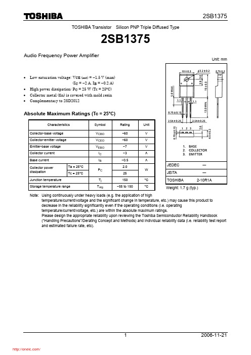
TOSHIBA Transistor Silicon PNP Triple Diffused Type
2SB1375
Audio Frequency Power Amplifier
2SB1375
Unit: mm
• Low saturation voltage: VCE (sat) = −1.5 V (max) (IC = −2 A, IB = −0.2 A)
DC current gain
Collector-emitter saturation voltage Base-emitter voltage Transition frequency Collector output capacitance
Symbol