TCS4615_DCDC_1.5A_SOT23-6
具备60V瞬态保护的36V输入、双输出跟踪、3.5A(10UT)、2.25MHz、降压型DC/DC转换器

7 一 一 一 吣 一 一 9 9 ^ 9 — 一 一 。 9 D 7 8 8 _ 0 7 8 8 O D _ D _ 9 。 D
l1 12 1- 8 】
【1 1 6 1- 8 ] f11 9 1- 8 】 【2 1 5 1- 8 ]
凌 力 尔特 公 司 ( ie r e h o g op rt n 推 出单 片双输 出降 压型 开关 稳 压 器 L 3 9 器件 可提 供 每 通道 高达 3 Ln a c n l yC roai ) F o o T 6 2. 该 .A 5 的连 续输 出 电流 T 6 2在 3 V 至 3 的输 入 电压 范 围 内x 作 , L 39 6V - 并具 有 6 瞬 态保 护 , 其 可 理 想 地 用 于 汽 车应 用 中 负载 0V 使
【2 12 1-5】
基 于XME GA的 便携 式 电解 质 分 析 仪 的 设 计
f —6] 0 1 7 6 [8 1 3 0—2] f8 1 7 o -2l
综 述
便 携 式 心 电 信 号 采集 电路 没训’
乍 钱血 库 湍度 监 控 系 统 的 研 究 及 实 现
显 示 光 电
基 于 I 乍 的新 供 暖 计 费 系 统 没 汁 C
超 高 频 R I 渎写 器设 计 FD
基 于 单 片 L 8 C S AT 9 5l ND1 C的MP 方 案 设计 3
医 疗 电 子
种 多 区域 视 频 监控 入 侵 检 测 报 警 方 法
基 于 单片 机 的 日历 时 钟 模 块 设 计 基 于 P I x rs实 时 视 频 采集 系统 的 设计 C p es E
(1 12 1- 7J
铲
铲
:
集成锂电池充电管理模 块、电机驱动模块、马达续流二极管、按键 档位控制、保护模块的全集成电机芯片

内置续流二极管马达持续驱动电流1.3A最大峰值电流2.6A可外置PMOS驱动更大电流0.6A充电电流充电红灯亮,充满绿灯亮放电绿灯亮,低电绿灯闪烁2.9V电池过放保护输出过流保护温度保护按键单击控制开关机SOT23-6小封装剃须刀、理发剪洁面仪便携式抽水泵电动牙刷、小风扇消毒枪手电筒、台灯XY3205是一款集成了锂电池充电管理模块、电机驱动模块、马达续流二极管、按键档位控制、保护模块的全集成电机驱动控制芯片,待机电流仅5uA。
XY3205充电电流为0.6A,充电红灯亮,充满绿灯亮,放电绿灯亮,低电绿灯闪烁提示。
XY3205最大输出电流为1.3A,也可以通过外扩PMOS管实现大于1.3A的应用场合。
XY3205通过按键单击控制输出开关,单击开机、再次单击关机。
XY3205XY32052.6A SOT23-63K/盘XY3205LXY3205L1.8A SOT23-63K/盘XY3005M SOT23-60.8A剃须刀/理发剪等1档,充电闪充满灭,放电时放电灯亮,低电时充电灯闪XY3106M SOP81A剃须刀/理发剪等1档,充电闪充满灭,放电时放电灯亮,低电时充电灯闪XY3205SOT23-60.6A剃须刀/理发剪等1档按键控制,充电亮红灯充满转绿灯,放电绿灯亮,低电绿灯闪XY3205E SOT23-60.6A剃须刀/理发剪等使能控制,充电亮红灯充满转绿灯,放电绿灯亮,低电绿灯闪XY3206SOP80.6A/1A剃须刀/小风扇等1档/3档,充电亮红灯充满转绿灯,放电绿灯亮,低电绿灯闪XY3207SOP80.3A-1A抽水泵/洁面仪等使能触发,使能为低后维持工作时间18S/36S/72S可选,充电闪充满灭,放电时放电灯亮,低电时充电灯闪XY3208SOP80.3A-1A剃须刀/电动牙刷使能控制,充电闪充满灭,放电时放电灯亮,低电时充电灯闪XY3306SOT23-60.6A小风扇等3档,50%-75%-100%-OFF,充电亮红灯充满转绿灯,放电绿灯亮,低电绿灯闪XY3307SOP80.3A电动牙刷等3档,100%-75%-50%-OFF,充电亮红灯充满转绿灯,放电绿灯亮,低电绿灯闪,带3档位指示灯C3可以根据电机堵转电流大小选择不同容值电容,若堵转电流小于2A,可以使用0.1uF,若堵转电流在2A-3A之间,则使用0.47uf,若大于3A,则使用2.2uf。
TLV62565(SOT23-5_1.5A)

VINVOUT1.8VL1ProductFolderSample &BuyTechnicalDocumentsTools &SoftwareSupport &CommunityTLV62565,TLV62566SLVSBC1B–OCTOBER2013–REVISED DECEMBER2014 TLV6256x1.5-A High Efficiency Step-Down Converters in SOT-235-Pin Package1Features3DescriptionThe TLV62565/6devices are synchronous step-down • 2.7-V to5.5-V Input Voltage Rangeconverters optimized for small solution size and high • 1.5-MHz Typical Switching Frequency efficiency.The devices integrate switches capable of•Output Current up to1.5A(Max)delivering an output current up to1.5A.•Adaptive On-Time Current Control The devices are based on an adaptive on time with •Power Save Mode for Light Load Efficiency valley current mode control scheme.Typicaloperating frequency is1.5MHz at medium to heavy •50-µA Operating Quiescent Currentloads.The devices are optimized to achieve very low •Up to95%Efficiencyoutput voltage ripple even with small external •Over Current Protection components and feature an excellent load transientresponse.•95%Maximum Duty Cycle•Excellent AC and Transient Load Response During a light load,the TLV62565/6automaticallyenter into Power Save Mode at the lowest quiescent •Power Good Output,TLV62566current(50μA typ)to maintain high efficiency over •Internal Soft Startup of250µs(Typ)the entire load current range.In shutdown,the •Adjustable Output Voltage current consumption is reduced to less than1μA.•Thermal Shutdown ProtectionThe TLV62565/6provide an adjustable output voltage •Available in SOT-235-Pin Package via an external resistor divider.The output voltagestart-up ramp is controlled by an internal soft start, 2Applications typically250µs.Power sequencing is possible byconfiguring the Enable(TLV62565)and Power Good •Portable Devices(TLV62566)pins.Other features like over current •DSL Modems protection and over temperature protection are built-•Hard Disk Drivers in.The TLV62565/6devices are available in a SOT-235-pin package.•Set Top Box•Tablet Device Information(1)PART NUMBER PACKAGE BODY SIZE(NOM)TLV62565,SOT-23(5) 2.90mm×1.60mmTLV62566(1)For all available packages,see the orderable addendum atthe end of the datasheet.4Simplified SchematicEfficiency vs Load CurrentTLV62565,TLV62566SLVSBC1B–OCTOBER2013–REVISED Table of Contents10.3Feature Description (11)1Features (1)10.4Device Functional Modes (12)2Applications (1)11Application and Implementation (13)3Description (1)11.1Application Information (13)4Simplified Schematic (1)11.2Typical Application (13)5Revision History (2)12Power Supply Recommendations (17)6Device Comparison Table (3)13Layout (18)7Pin Configuration and Functions (3)13.1Layout Guidelines (18)8Specifications (4)13.2Layout Example (18)8.1Absolute Maximum Ratings (4)13.3Thermal Considerations (18)8.2ESD Ratings (4)14Device and Documentation Support (19)8.3Recommended Operating Conditions (4)14.1Device Support (19)8.4Thermal Information (4)14.2Documentation Support (19)8.5Electrical Characteristics (5)14.3Related Links (19)8.6Typical Characteristics (6)14.4Trademarks (19)9Parameter Measurement Information (8)14.5Electrostatic Discharge Caution (19)10Detailed Description (9)14.6Glossary (19)10.1Overview (9)15Mechanical,Packaging,and Orderable10.2Functional Block Diagrams...................................10Information.. (19)5Revision HistoryNOTE:Page numbers for previous revisions may differ from page numbers in the current version.Changes from Revision A(November2014)to Revision B Page •Added Storage temperature to Absolute Maximum Ratings (4)•Changed Handling Ratings to ESD Ratings (4)•Deleted Storage temperature from ESD Ratings (4)•Changed Thermal Information to Thermal Considerations and moved to Layout section (18)Changes from Original(October2013)to Revision A Page •Changed Added Handling Rating table,Feature Description section,Device Functional Modes,Application and Implementation section,Power Supply Recommendations section,Layout section,Device and DocumentationSupport section,and Mechanical,Packaging,and Orderable Information section (1)•Added"T A=-40°C to85°C"to the V FB,Feedback regulation voltage Test Conditions (5)•Added V FB,Feedback regulation voltage Test Conditions and values for"PWM operation,T A=85°C" (5)2Submit Documentation Feedback Copyright©2013–2014,Texas Instruments Incorporated12345VIN SWGND FB EN/PG TLV62565,TLV62566SLVSBC1B –OCTOBER 2013–REVISED DECEMBER 20146Device Comparison TablePART NUMBER FUNCTIONTLV62566EN TLV62566PG7Pin Configuration and Functions5-Pin SOT-23DBV Package (Top View)Pin FunctionsPINNUMBERI/O/PWRDESCRIPTIONNAME TLV62565TLV62566Device enable logic input.Logic HIGH enables the device,logic low disables the device EN 1—I and turns it into shutdown.Feedback pin for the internal control loop.Connect this pin to the external feedback FB 55I divider.GND 22PWR Ground pin.Power Good open drain output.This pin is high impedance if the output voltage is within PG —1O regulation.It is pulled low if the output is below its nominal value.It is also in logic low when V IN below UVLO or thermal shutdown triggers.Switch pin connected to the internal MOSFET switches and inductor terminal.Connect SW 33PWR the inductor of the output filter to this pin.VIN44PWRPower supply voltage input.Copyright ©2013–2014,Texas Instruments Incorporated Submit Documentation Feedback 3TLV62565,TLV62566SLVSBC1B–OCTOBER2013–REVISED 8Specifications8.1Absolute Maximum RatingsOver operating free-air temperature range(unless otherwise noted)(1)MIN MAX UNITVIN,EN,PG–0.37V Voltage(2)SW–0.3V IN+0.3VFB–0.3 3.6V Sink current,I PG PG660µA Continuous total power dissipation See Thermal InformationOperating junction temperature,T J–40150°C Storage temperature,T stg–65150°C (1)Stresses beyond those listed under absolute maximum ratings may cause permanent damage to the device.These are stress ratingsonly and functional operation of the device at these or any other conditions beyond those indicated under recommended operating conditions is not implied.Exposure to absolute–maximum–rated conditions for extended periods may affect device reliability.(2)All voltage values are with respect to network ground terminal.8.2ESD RatingsVALUE UNIT Human-body model(HBM),per ANSI/ESDA/JEDEC JS-001(1)±2000V ElectrostaticV(ESD)discharge Charged-device model(CDM),per JEDEC specification JESD22-C101(2)±500V(1)JEDEC document JEP155states that500-V HBM allows safe manufacturing with a standard ESD control process.(2)JEDEC document JEP157states that250-V CDM allows safe manufacturing with a standard ESD control process.8.3Recommended Operating Conditions(1)MIN TYP MAX UNIT V IN Input voltage,VIN 2.7 5.5VT A Operating ambient temperature–4085°C (1)Refer to the Application and Implementation section for further information.8.4Thermal InformationTLV62565,TLV62566THERMAL METRIC(1)UNITDBV(5Pins)RθJA Junction-to-ambient thermal resistance208.3RθJC(top)Junction-to-case(top)thermal resistance73.7RθJB Junction-to-board thermal resistance36.1°C/WψJT Junction-to-top characterization parameter 2.3ψJB Junction-to-board characterization parameter35.3RθJC(bot)Junction-to-case(bottom)thermal resistance N/A(1)For more information about traditional and new thermal metrics,see the IC Package Thermal Metrics application report,SPRA953.4Submit Documentation Feedback Copyright©2013–2014,Texas Instruments IncorporatedTLV62565,TLV62566 SLVSBC1B–OCTOBER2013–REVISED DECEMBER20148.5Electrical CharacteristicsOver recommended free-air temperature range,V IN=3.6V,T A=-40°C to85°C,typical values are at T A=25°C(unless otherwise noted)PARAMETER TEST CONDITIONS MIN TYP MAX UNIT SUPPLYV IN Input voltage 2.7 5.5VI Q Quiescent current into VIN pin I OUT=0mA,Not switching50uAUnder voltage lock out V IN falling 2.2 2.3VV UVLOUnder voltage lock out hysteresis200mVThermal shutdown Junction temperature rising150T JSD°C Thermal shutdown hysteresis Junction temperature falling below T JSD20LOGIC INTERFACE,TLV62565V IH High-level input voltage 2.7V≤V IN≤5.5V 1.2VV IL Low-level input voltage 2.7V≤V IN≤5.5V0.4VI SD Shutdown current into VIN pin EN=LOW0.11µAI EN,LKG EN leakage current0.010.16µA POWER GOOD,TLV62566Power Good low threshold V FB falling referenced to V FB nominal90%V PGPower Good high threshold V FB risng referenced to V FB nominal95%V L Low level voltage I sink=500µA0.4VI PG,LKG PG Leakage current V PG=5.0V0.010.17µA OUTPUTV OUT Output voltage0.6D MAX.V IN VPWM operation,T A=-40°C to85°C0.5880.60.612VV FB Feedback regulation voltage PWM operation,T A=85°C0.5940.60.606VPFM comparator threshold0.9%I FB Feedback input bias current V FB=0.6V10100nAHigh-side FET on resistance I SW=500mA,V IN=3.6V173R DS(on)mΩLow-side FET on resistance I SW=500mA,V IN=3.6V105I LIM,LS Low-side FET valley current limit 1.5AI LIM,HS High-side FET peak current limit 1.8Af SW Switching frequency 1.5MHzD MAX Maximum duty cycle95%t OFF,MIN Minimum off time40ns Copyright©2013–2014,Texas Instruments Incorporated Submit Documentation Feedback5TLV62565,TLV62566SLVSBC1B–OCTOBER2013–REVISED 8.6Typical CharacteristicsTable1.Table of GraphsFIGURE vs Load current(V OUT=1.8V,V IN=2.7V,3.6V,5.5V)Figure1 Efficiency vs Load current(V OUT=1.2V,V IN=2.7V,3.6V,5.5V)Figure2 vs Load current(V OUT=3.3V,V IN=4.2V,5.5V)Figure3vs Input voltage(Line regulation,V OUT=1.8V,Load=0.5A,1A,1.5A)Figure4 Output voltagevs Load current(Load regulation,V OUT=1.8V,V IN=2.7V,3.6V,5.5V)Figure5 Quiescent current vs Input voltage Figure6vs Input voltage,High-Side FET Figure7R DS(on)vs Input voltage,Low-Side FET Figure8 Switching frequency vs Load current,V OUT=1.8V Figure96Submit Documentation Feedback Copyright©2013–2014,Texas Instruments IncorporatedTLV62565,TLV62566 SLVSBC1B–OCTOBER2013–REVISED DECEMBER2014Copyright©2013–2014,Texas Instruments Incorporated Submit Documentation Feedback7V INV OUTL1TLV62565,TLV62566SLVSBC1B –OCTOBER 2013–REVISED DECEMBER 20149Parameter Measurement InformationTable 2.List of ComponentsREFERENCEDESCRIPTIONMANUFACTURERC1 4.7µF,Ceramic Capacitor,6.3V,X5R,size 0603,GRM188R60J475ME84Murata C210µF,Ceramic Capacitor,6.3V,X5R,size 0603,GRM188R60J106ME84Murata L1 2.2µH,Power Inductor,2.5A,size 4mmx4mm,LQH44PN2R2MP0Murata R1,R2Chip resistor,1%,size 0603Std.8Submit Documentation Feedback Copyright ©2013–2014,Texas Instruments IncorporatedPWMValley LS TLV62565,TLV62566SLVSBC1B –OCTOBER 2013–REVISED DECEMBER 201410Detailed Description10.1OverviewThe TLV62565/6device family includes two high-efficiency synchronous step-down converters.Each device operates with an adaptive on-time control scheme,which is able to dynamically adjust the on-time duration based on the input voltage and output voltage so that it can achieve relative constant frequency operation.The device operates at typically 1.5-MHz frequency pulse width modulation (PWM)at moderate to heavy load currents.Based on the V IN /V OUT ratio,a simple circuit sets the required on time for the high-side MOSFET.It makes the switching frequency relatively constant regardless of the variation of input voltage,output voltage,and load current.At the beginning of each switching cycle,the high-side switch is turned on and the inductor current ramps up to a peak current that is defined by on time and inductance.In the second phase,once the on time expires,the high-side switch is turned off while the low-side switch is being turned on.The current through the inductor then decays until triggering the valley current limit determined by the output of the error amplifier.Once this occurs,the on timer is set to turn the high-side switch back on again and the cycle is repeated.The TLV62565/6device family offers excellent load transient response with a unique fast response constant on-time valley current mode.The switching frequency changes during load transition so that the output voltage comes back in regulation faster than a traditional fixed PWM control scheme.Figure 10shows the operation principles of the load transient response of the TLV62565/6.Internal loop compensation is integrated which simplifies the design process while minimizing the number of external components.At light load currents the device automatically operates in Power Save Mode with pulse frequency modulation (PFM).Figure 10.Operation in Load TransientCopyright ©2013–2014,Texas Instruments Incorporated Submit Documentation Feedback 9V INPGGNDFBSWV INGNDFBENSWTLV62565,TLV62566SLVSBC1B –OCTOBER 2013–REVISED DECEMBER 201410.2Functional Block DiagramsFigure 11.TLV62565Functional Block DiagramFigure 12.TLV62566Functional Block Diagram10Submit Documentation Feedback Copyright ©2013–2014,Texas Instruments IncorporatedOutput tTLV62565,TLV62566SLVSBC1B –OCTOBER 2013–REVISED DECEMBER 201410.3Feature Description10.3.1Power Save ModeThe device integrates a Power Save Mode with PFM to improve efficiency at light load.In Power Save Mode,the device only switches when the output voltage trips below a set threshold voltage.It ramps up the output voltage with several pulses and stops switching when the output voltage is higher than the set threshold voltage.PFM is exited and PWM mode entered in case the output current can no longer be supported in Power Save Mode.The threshold of the PFM comparator is typically 0.9%higher than the normal reference voltage.Figure 13shows the details of PFM/PWM mode transition.Figure 13.Output Voltage in PFM/PWM Mode10.3.2Enabling/Disabling the DeviceThe device is enabled by setting the EN input to a logic HIGH.Accordingly,a logic LOW disables the device.If the device is enabled,the internal power stage starts switching and regulates the output voltage to the set point voltage.The EN input must be terminated and should not be left floating.10.3.3Soft StartAfter enabling the device,internal soft-start circuitry monotonically ramps up the output voltage which reaches nominal output voltage during a soft-start time of 250µs (typical).This avoids excessive inrush current and creates a smooth output voltage rise slope.It also prevents excessive voltage drops of primary cells and rechargeable batteries with high internal impedance.If the output voltage is not reached within the soft-start time,such as in the case of a heavy load,the converter enters regular operation.The TLV62565/6are able to start into a pre-biased output capacitor.The converter starts with the applied bias voltage and ramps the output voltage to its nominal value.10.3.4Switch Current LimitThe switch current limit prevents the device from high inductor current and drawing excessive current from a battery or input voltage rail.Excessive current might occur with a heavy load or shorted output circuit condition.The TLV62565/6adopt valley current control by sensing the current of the low-side MOSFET.Once the low-side valley switch current limit is tripped,the low-side MOSFET is turned off and limits the inductor's valley current.The high-side current is also limited which is determined by the on time of the high-side MOSFET and inductor value calculated by Equation 1.For example,with 3.6V IN to 1.8V OUT and 2.2-µH specification,the peak current limit is approximately 1.97A with a typical valley current limit of 1.7A.Additionally,there is a secondary high-side current limit (typical 2A)to prevent the current from going too high,which is shown in Figure 14.Due to the internal propagation delay,the real current limit value might be higher than the static current limit in the electrical characteristics table.Copyright ©2013–2014,Texas Instruments Incorporated Submit Documentation Feedback 11SWOUT L L IT VALLEY,LIM PEAK,LIMIT f D)(L V ΔI ΔI I I -´=+=1Inductortload currentlimit TLV62565,TLV62566SLVSBC1B –OCTOBER 2013–REVISED DECEMBER 2014Feature Description (continued)Figure 14.Switch Current Limitwhere:•I PEAK,LIMIT is the high-side peak current limit •I VALLEY,LIMIT is the low-side valley current limit(1)10.3.5Power GoodThe TLV62566integrates a Power Good output going low when the output voltage is below its nominal value.The Power Good output stays high impedance once the output is above 95%of the regulated voltage and is low once the output voltage falls below typically 90%of the regulated voltage.The PG pin is an open drain output and is specified to sink typically up to 0.5mA.The Power Good output requires a pull-up resistor connected to any voltage lower than 5.5V.When the device is off due to UVLO or thermal shutdown,the PG pin is pulled to logic low.10.4Device Functional Modes10.4.1Under Voltage LockoutTo avoid mis-operation of the device at low input voltages,under voltage lockout is implemented that shuts down the device at voltages lower than V UVLO with V HYS_UVLO hysteresis.10.4.2Thermal ShutdownThe device enters thermal shutdown once the junction temperature exceeds typically T JSD .Once the device temperature falls below the threshold with hysteresis,the device returns to normal operation automatically.Power Good is pulled low when thermal protection is triggered.12Submit Documentation Feedback Copyright ©2013–2014,Texas Instruments IncorporatedVINVOUT1.2VL1TLV62565,TLV62566 SLVSBC1B–OCTOBER2013–REVISED DECEMBER2014 11Application and ImplementationNOTEInformation in the following applications sections is not part of the TI componentspecification,and TI does not warrant its accuracy or completeness.TI’s customers areresponsible for determining suitability of components for their purposes.Customers shouldvalidate and test their design implementation to confirm system functionality.11.1Application InformationThe TLV6256x devices are synchronous step-down converters optimized for small solution size and high efficiency.The devices integrate switches capable of delivering an output current up to1.5A.11.2Typical ApplicationTLV625652.7-V to5.5-V input,1.2-V output converter.Figure15.TLV625651.2-V Output Application11.2.1Design Requirements11.2.1.1Output Filter DesignThe inductor and output capacitor together provide a low-pass frequency filter.To simplify this process,Table3 outlines possible inductor and capacitor value combinations.Table3.Matrix of Output Capacitor and Inductor CombinationsC OUT[µF](2)(3)L[µH](1)4.710224710012.2+(4)+(4)+(4)4.7(1)Inductor tolerance and current de-rating is anticipated.The effective inductance can vary by+20%and-30%.(2)Capacitance tolerance and bias voltage de-rating is anticipated.The effective capacitance can vary by+20%and-50%.(3)For low output voltage applications(≤1.2V),more output capacitance is recommended(usually≥22µF)for smaller ripple.(4)Typical application configuration.'+'indicates recommended filter combinations.Copyright©2013–2014,Texas Instruments Incorporated Submit Documentation Feedback13SWINOUT OUT L LMAX ,OUT MAX ,L f L V V 1V I 2II I ´-´=D D +=TLV62565,TLV62566SLVSBC1B –OCTOBER 2013–REVISED DECEMBER 201411.2.1.2Inductor SelectionThe main parameters for inductor selection is inductor value and then saturation current of the inductor.To calculate the maximum inductor current under static load conditions,Equation 2is given:where:•I OUT,MAX is the maximum output current •ΔI L is the inductor current ripple •f SW is the switching frequency •L is the inductor value(2)It is recommended to choose a saturation current for the inductor that is approximately 20%to 30%higher than I L,MAX .In addition,DC resistance and size should also be taken into account when selecting an appropriate inductor.The recommended inductors are listed in Table 4.Table 4.List of Recommended InductorsINDUCTANCECURRENT RATINGDIMENSIONS DC RESISTANCETYPE MANUFACTURER[µH][mA]L x W x H [mm 3][m Ωtyp]2.225004x3.7x 1.6549LQH44PN2R2MP0Murata 2.230004x 4x 1.850NRS4018T2R2MDGJTaiyo Yuden11.2.1.3Input and Output Capacitor SelectionThe input capacitor is the low impedance energy source for the converter that helps provide stable operation.The closer the input capacitor is placed to the V IN and GND pins,the lower the switch ring.A low ESR multilayer ceramic capacitor is recommended for best filtering.For most applications,4.7-µF input capacitance is sufficient;a larger value reduces input voltage ripple.The architecture of the TLV62565/6allow use of tiny ceramic-type output capacitors with low equivalent series resistance (ESR).These capacitors provide low output voltage ripple and are thus recommended.To keep its resistance up to high frequencies and to achieve narrow capacitance variation with temperature,it is recommended to use X7R or X5R dielectric.The TLV62565/6are designed to operate with an output capacitance of 10µF to 47µF,as outlined in Table 3.14Submit Documentation Feedback Copyright ©2013–2014,Texas Instruments Incorporated)16.0(2)1(21-´=-´=V V R V VR R OUT FB OUT W ===k AV I V R FB FB 12056.02m ÷øöçèæ+´=÷øöçèæ+´=2116.0211R R V R R V V FB OUT TLV62565,TLV62566SLVSBC1B –OCTOBER 2013–REVISED DECEMBER 201411.2.2Detailed Design Procedure 11.2.2.1Setting the Output VoltageAn external resistor divider is used to set output voltage.By selecting R1and R2,the output voltage is programmed to the desired value.When the output voltage is regulated,the typical voltage at the FB pin is V FB .Equation 3,Equation 4,and Equation 5can be used to calculate R1and R2.When sizing R2,in order to achieve low quiescent current and acceptable noise sensitivity,use a minimum of 5μA for the feedback current I FB .Larger currents through R2improve noise sensitivity and output voltage accuracy but increase current consumption.(3)(4)(5)11.2.2.2Loop StabilityThe first step of circuit and stability evaluation is to look from a steady-state perspective at the following signals:•Switching node,SW •Inductor current,I L•Output ripple voltage,V OUT(AC)These are the basic signals that need to be measured when evaluating a switching converter.When the switching waveform shows large duty cycle jitter or the output voltage or inductor current shows oscillations,the regulation loop may be unstable.This is often a result of board layout and/or L-C combination.Applications with the recommended L-C combinations in Table 3are designed for good loop stability as well as fast load transient response.As a next step in the evaluation of the regulation loop,the load transient response is illustrated.The TLV62565/6use a constant on time with valley current mode control,so the on time of the high-side MOSFET is relatively consistent from cycle to cycle when a load transient occurs.Whereas the off time adjusts dynamically in accordance with the instantaneous load change and brings V OUT back to the regulated value.During recovery time,V OUT can be monitored for settling time,overshoot,or ringing which helps judge the stability of the converter.Without any ringing,the loop usually has more than 45°of phase margin.Copyright ©2013–2014,Texas Instruments Incorporated Submit Documentation Feedback 15oA/div0.1 V/div oA/divinductor V V = 1.8 VIN O = 3.6 V L=2.2 uH, C =10 uF Load: 1.3A to 0.3Ao 4.0 µs/divG008EN 1 V/div V V = 1.8 VIN O = 3.6 V 400 µs/divG004SW 2 V/div V V = 1.8 V/10mAIN O = 3.6 V10 µs/divG003oA/div0.1 V/div oA/divinductor V V = 1.8 VIN O = 3.6 V L=2.2 uH,C =10 uF Load: 0.3A to 1.3Ao 4.0 µs/divG007V V = 1.8 VIN O = 3.6 V 0.4 µs/divG001SW 2 V/div V V = 1.8 V/100mAIN O = 3.6 V2.0 µs/divG002TLV62565,TLV62566SLVSBC1B –OCTOBER 2013–REVISED DECEMBER 201411.2.3Application Performance CurvesFigure 16.Typical Application (PWM Mode)Figure 17.Typical Application (PFM Mode)Figure 18.Typical Application (PFM Mode)Figure 19.Load TransientFigure 20.Load Transient Figure 21.Start Up16Submit Documentation Feedback Copyright ©2013–2014,Texas Instruments IncorporatedPG 1 V/div1 V/div o 1A/div inductor V V = 1.8 V IN O = 3.6 V Load= 0A400 µs/divG005IN 5 V/divA/divV V = 1.8 VIN O = 3.6 V 2.0 µs/divG006TLV62565,TLV62566SLVSBC1B –OCTOBER 2013–REVISED DECEMBER 2014Figure 22.Start Up (Power Good)Figure 23.Short Circuit Protection12Power Supply RecommendationsThe power supply to the TLV62565and TLV62566needs to have a current rating according to the supply voltage,output voltage and output current of the TLV62565and TLV62566.Copyright ©2013–2014,Texas Instruments Incorporated Submit Documentation Feedback 17TLV62565,TLV62566SLVSBC1B–OCTOBER2013–REVISED 13Layout13.1Layout GuidelinesThe PCB layout is an important step to maintain the high performance of the TLV62565devices.•The input/output capacitors and the inductor should be placed as close as possible to the IC.•This keeps the traces short.Routing these traces direct and wide results in low trace resistance and low parasitic inductance.•A common power GND should be used.•The low side of the input and output capacitors must be connected properly to the power GND to avoid a GND potential shift.•The sense traces connected to FB is a signal trace.•Special care should be taken to avoid noise being induced.By a direct routing,parasitic inductance can be kept small.•GND layers might be used for shielding.•Keep these traces away from SW nodes.13.2Note:13.3typically requires special coupling,airflow, convection dissipation limits of a givenTwo basic approaches for enhancing thermal performance are listed below:•Improving the power dissipation capability of the PCB design•Introducing airflow in the systemFor more details on how to use the thermal parameters,see the application notes:Thermal Characteristics Application Notes SZZA017and SPRA953.18Submit Documentation Feedback Copyright©2013–2014,Texas Instruments IncorporatedTLV62565,TLV62566 SLVSBC1B–OCTOBER2013–REVISED DECEMBER201414Device and Documentation Support14.1Device Support14.1.1Third-Party Products DisclaimerTI'S PUBLICATION OF INFORMATION REGARDING THIRD-PARTY PRODUCTS OR SERVICES DOES NOT CONSTITUTE AN ENDORSEMENT REGARDING THE SUITABILITY OF SUCH PRODUCTS OR SERVICES OR A WARRANTY,REPRESENTATION OR ENDORSEMENT OF SUCH PRODUCTS OR SERVICES,EITHER ALONE OR IN COMBINATION WITH ANY TI PRODUCT OR SERVICE.14.2Documentation Support14.2.1Related DocumentationSemiconductor and IC Package Thermal Metrics Application Report(SPRA953)Thermal Characteristics of Linear and Logic Packages Using JEDEC PCB Designs Application Report (SZZA017)14.3Related LinksThe table below lists quick access links.Categories include technical documents,support and community resources,tools and software,and quick access to sample or buy.Table5.Related LinksTECHNICAL TOOLS&SUPPORT& PARTS PRODUCT FOLDER SAMPLE&BUYDOCUMENTS SOFTWARE COMMUNITY TLV62565Click here Click here Click here Click here Click here TLV62566Click here Click here Click here Click here Click here 14.4TrademarksAll trademarks are the property of their respective owners.14.5Electrostatic Discharge CautionThese devices have limited built-in ESD protection.The leads should be shorted together or the device placed in conductive foam during storage or handling to prevent electrostatic damage to the MOS gates.14.6GlossarySLYZ022—TI Glossary.This glossary lists and explains terms,acronyms,and definitions.15Mechanical,Packaging,and Orderable InformationThe following pages include mechanical,packaging,and orderable information.This information is the most current data available for the designated devices.This data is subject to change without notice and revision of this document.For browser-based versions of this data sheet,refer to the left-hand navigation.Copyright©2013–2014,Texas Instruments Incorporated Submit Documentation Feedback19。
LED显示驱动IC功能解析
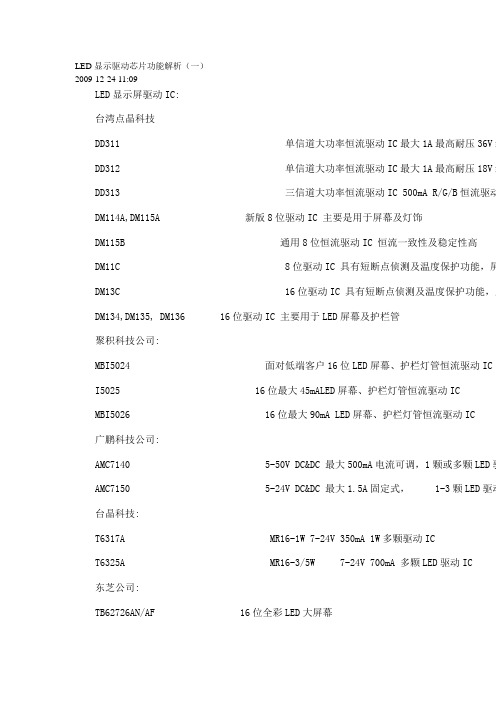
LED显示驱动芯片功能解析(一)2009-12-24 11:09LED显示屏驱动IC:台湾点晶科技DD311 单信道大功率恒流驱动IC最大1A最高耐压36V线DD312 单信道大功率恒流驱动IC最大1A最高耐压18V线DD313 三信道大功率恒流驱动IC 500mA R/G/B恒流驱动DM114A,DM115A 新版8位驱动IC 主要是用于屏幕及灯饰DM115B 通用8位恒流驱动IC 恒流一致性及稳定性高DM11C 8位驱动IC 具有短断点侦测及温度保护功能,屏DM13C 16位驱动IC 具有短断点侦测及温度保护功能,屏DM134,DM135, DM136 16位驱动IC 主要用于LED屏幕及护栏管聚积科技公司:MBI5024 面对低端客户16位LED屏幕、护栏灯管恒流驱动IC I5025 16位最大45mALED屏幕、护栏灯管恒流驱动ICMBI5026 16位最大90mA LED屏幕、护栏灯管恒流驱动IC广鹏科技公司:AMC7140 5-50V DC&DC 最大500mA电流可调,1颗或多颗LED驱AMC7150 5-24V DC&DC 最大1.5A固定式, 1-3颗LED驱动台晶科技:T6317A MR16-1W 7-24V 350mA 1W多颗驱动ICT6325A MR16-3/5W 7-24V 700mA 多颗LED驱动IC东芝公司:TB62726AN/AF 16位全彩LED大屏幕TB62726ANG/AFG 16位全彩LED大屏幕彩LED大屏幕带断、短路侦测及温度保护IR 国际整流器公司:IRS2540 200V市电直驱1W多颗LED驱动IC,500mA IRS2541美国超科公司 (Supertex):HV9910 高压大功率直驱LED恒流器件HV9931 高压双向检测大功率直驱LED恒流IC,可PWM灰度调节杭州士兰微电子有限公司:SB16726 16位恒流驱动全彩屏幕ICSC16722 可级连、大电流输出的专用LED驱动电路SB42351 350mA低压差白光固定式LED驱动芯片SB42510 PWM控制、1A白光LED恒流芯片QX9910 大功率20MA-2A,2.5V-220V直驱恒流ICQX9920 2.5V-220V可编程LED 驱动电流,编程范围为10mA到1A QX62726 LED大屏幕16位移位恒流驱动SM16126B 16位恒流移位寄存器,应用于LED屏幕及灯饰产品LED屏幕配套部分逻辑IC,飞利浦些列:74HC595D 逻辑8位移位寄存器74HC245D 3态8总线收发器74HC138D 3-8线译码器、多路转换74HC164D 8位移位寄存器(串进并出)74HC04D 逻辑6非门74HC08D 逻辑6非门驱动器74HC244D 8缓冲/线驱动/线接收(3态)LED屏幕配套部分 MOS管:MT4953 台湾茂钿APM4953 台湾茂达GE4953 深圳捷托74HC5951 、描述 74HC595是硅结构的CMOS器件,兼容低电压TTL电路,遵守JEDEC标准。
3.7V降压3V,5V降压3V的升降压电路和芯片

3.7V 降压3V ,5V 降压3V 高效率降压芯片,超低功耗稳压芯片,的几款降压IC ,的降压芯片和LDO ,芯片选型说明,降压芯片,稳压芯片,电路图芯片3.7V 降压3V ,5V 降压3V 的电路和芯片解决方案有2种:1,降压芯片,2,LDO 芯片。
解决方案1,降压芯片3.7V 大家都知道是锂电池多,确实是3.7V 锂电池的话,锂电池的充满电和放电后的电压变化是在:3V-4.2V 之间,带保护板的锂电池。
3V 输入降压3V 的话,降压芯片的占空比都是95%以上,输出电压能在2.8V 左右。
一般都可以接受就不用到升降压芯片PW2228A 了.5V 输入分2种情况,1是稳定的5V 电源,2是不稳定的5V 电源,有时电压会高于5V ,或者经常拔插尖峰电压高于6V 等。
就需要更高输入的降压芯片来完成工作。
DC-DC 降压产品输入电压 输出电压 输出电流 频率 封装 PW2058 2.0V ~6.0V 1V ~5V 0.8A 1.5MHz SOT23-5 PW2051 2.5V ~5.5V 1V ~5V 1.5A 1.5MHz SOT23-5 PW2052 2.5V ~5.5V 1V ~5V 2.0A 1.0 MHz SOT23-5 PW2053 2.5V ~5.5V 1V ~5V 3.0A 1.0 MHz SOT23-5 PW2162 4.5V ~16V 1V ~15V 2A 600KHZ SOT23-6 PW2163 4.5V ~16V 1V ~15V 3A 600KHZ SOT23-6 PW2205 4.5V ~20V 1V ~15V 5A 340KHZ SOP8-EP PW2312 4.0V ~30V 1V ~28V 1.2A 1.4 MHz SOT23-6 PW2330 4.5V ~30V 1V ~28V 3A 130KHz SOP8 PW2431 4.5V ~40V 1V ~30V 3A 340KHz SOP8-EP PW2558 4.5V ~55V 1.25V ~30V 0.8A 1.2 MHz SOT23-6 PW2608 5.5V ~60V 1.5-30V 0.8A 0.3-1Mhz SOP8-EPPW2815 4.5V ~80V 1.5V ~30V 1.5A 400KHZ SOP8-EP PW2906 12V ~90V 1.25V ~20V 0.6A 150KHZ SOP8-EP PW2902 8V ~90V 5V ~30V 2A 140KHZ SOP8-EP PW2153 8V ~140V5V ~30V4A140KHZSOP8。
常用开关电源芯片大全
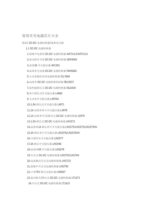
常用开关电源芯片大全第1章DC-DC电源转换器/基准电压源1.1 DC-DC电源转换器1.低噪声电荷泵DC-DC电源转换器AAT3113/AAT31142.低功耗开关型DC-DC电源转换器ADP30003.高效3A开关稳压器AP15014.高效率无电感DC-DC电源转换器FAN56605.小功率极性反转电源转换器ICL76606.高效率DC-DC电源转换控制器IRU30377.高性能降压式DC-DC电源转换器ISL64208.单片降压式开关稳压器L49609.大功率开关稳压器L4970A10.1.5A降压式开关稳压器L497111.2A高效率单片开关稳压器L497812.1A高效率升压/降压式DC-DC电源转换器L597013.1.5A降压式DC-DC电源转换器LM157214.高效率1A降压单片开关稳压器LM1575/LM2575/LM2575HV15.3A降压单片开关稳压器LM2576/LM2576HV16.可调升压开关稳压器LM257717.3A降压开关稳压器LM259618.高效率5A开关稳压器LM267819.升压式DC-DC电源转换器LM2703/LM270420.电流模式升压式电源转换器LM273321.低噪声升压式电源转换器LM275022.小型75V降压式稳压器LM500723.低功耗升/降压式DC-DC电源转换器LT107324.升压式DC-DC电源转换器LT161525.隔离式开关稳压器LT172526.低功耗升压电荷泵LT175127.大电流高频降压式DC-DC电源转换器LT176528.大电流升压转换器LT193529.高效升压式电荷泵LT193730.高压输入降压式电源转换器LT195631.1.5A升压式电源转换器LT196132.高压升/降压式电源转换器LT343333.单片3A升压式DC-DC电源转换器LT343634.通用升压式DC-DC电源转换器LT346035.高效率低功耗升压式电源转换器LT346436.1.1A升压式DC-DC电源转换器LT346737.大电流高效率升压式DC-DC电源转换器LT378238.微型低功耗电源转换器LTC175439.1.5A单片同步降压式稳压器LTC187540.低噪声高效率降压式电荷泵LTC191141.低噪声电荷泵LTC3200/LTC3200-542.无电感的降压式DC-DC电源转换器LTC325143.双输出/低噪声/降压式电荷泵LTC325244.同步整流/升压式DC-DC电源转换器LTC340145.低功耗同步整流升压式DC-DC电源转换器LTC340246.同步整流降压式DC-DC电源转换器LTC340547.双路同步降压式DC-DC电源转换器LTC340748.高效率同步降压式DC-DC电源转换器LTC341649.微型2A升压式DC-DC电源转换器LTC342650.2A两相电流升压式DC-DC电源转换器LTC342851.单电感升/降压式DC-DC电源转换器LTC344052.大电流升/降压式DC-DC电源转换器LTC344253.1.4A同步升压式DC-DC电源转换器LTC345854.直流同步降压式DC-DC电源转换器LTC370355.双输出降压式同步DC-DC电源转换控制器LTC373656.降压式同步DC-DC电源转换控制器LTC377057.双2相DC-DC电源同步控制器LTC380258.高性能升压式DC-DC电源转换器MAX1513/MAX151459.精简型升压式DC-DC电源转换器MAX1522/MAX1523/MAX152460.高效率40V升压式DC-DC电源转换器MAX1553/MAX155461.高效率升压式LED电压调节器MAX1561/MAX159962.高效率5路输出DC-DC电源转换器MAX156563.双输出升压式DC-DC电源转换器MAX1582/MAX1582Y64.驱动白光LED的升压式DC-DC电源转换器MAX158365.高效率升压式DC-DC电源转换器MAX1642/MAX164366.2A降压式开关稳压器MAX164467.高效率升压式DC-DC电源转换器MAX1674/MAX1675/MAX167668.高效率双输出DC-DC电源转换器MAX167769.低噪声1A降压式DC-DC电源转换器MAX1684/MAX168570.高效率升压式DC-DC电源转换器MAX169871.高效率双输出降压式DC-DC电源转换器MAX171572.小体积升压式DC-DC电源转换器MAX1722/MAX1723/MAX172473.输出电流为50mA的降压式电荷泵MAX173074.升/降压式电荷泵MAX175975.高效率多路输出DC-DC电源转换器MAX180076.3A同步整流降压式稳压型MAX1830/MAX183177.双输出开关式LCD电源控制器MAX187878.电流模式升压式DC-DC电源转换器MAX189679.具有复位功能的升压式DC-DC电源转换器MAX194780.高效率PWM降压式稳压器MAX1992/MAX199381.大电流输出升压式DC-DC电源转换器MAX61882.低功耗升压或降压式DC-DC电源转换器MAX62983.PWM升压式DC-DC电源转换器MAX668/MAX66984.大电流PWM降压式开关稳压器MAX724/MAX72685.高效率升压式DC-DC电源转换器MAX756/MAX75786.高效率大电流DC-DC电源转换器MAX761/MAX76287.隔离式DC-DC电源转换器MAX8515/MAX8515A88.高性能24V升压式DC-DC电源转换器MAX872789.升/降压式DC-DC电源转换器MC33063A/MC34063A90.5A升压/降压/反向DC-DC电源转换器MC33167/MC3416791.低噪声无电感电荷泵MCP1252/MCP125392.高频脉宽调制降压稳压器MIC220393.大功率DC-DC升压电源转换器MIC229594.单片微型高压开关稳压器NCP1030/NCP103195.低功耗升压式DC-DC电源转换器NCP1400A96.高压DC-DC电源转换器NCP140397.单片微功率高频升压式DC-DC电源转换器NCP141098.同步整流PFM步进式DC-DC电源转换器NCP142199.高效率大电流开关电压调整器NCP1442/NCP1443/NCP1444/NCP1445100.新型双模式开关稳压器NCP1501101.高效率大电流输出DC-DC电源转换器NCP1550102.同步降压式DC-DC电源转换器NCP1570103.高效率升压式DC-DC电源转换器NCP5008/NCP5009104.大电流高速稳压器RT9173/RT9173A105.高效率升压式DC-DC电源转换器RT9262/RT9262A106.升压式DC-DC电源转换器SP6644/SP6645107.低功耗升压式DC-DC电源转换器SP6691108.新型高效率DC-DC电源转换器TPS54350109.无电感降压式电荷泵TPS6050x110.高效率升压式电源转换器TPS6101x111.28V恒流白色LED驱动器TPS61042112.具有LDO输出的升压式DC-DC电源转换器TPS6112x113.低噪声同步降压式DC-DC电源转换器TPS6200x114.三路高效率大功率DC-DC电源转换器TPS75003115.高效率DC-DC电源转换器UCC39421/UCC39422116.PWM控制升压式DC-DC电源转换器XC6371117.白光LED驱动专用DC-DC电源转换器XC9116118.500mA同步整流降压式DC-DC电源转换器XC9215/XC9216/XC9217119.稳压输出电荷泵XC9801/XC9802120.高效率升压式电源转换器ZXLB16001.2 线性/低压差稳压器121.具有可关断功能的多端稳压器BAXXX122.高压线性稳压器HIP5600123.多路输出稳压器KA7630/KA7631124.三端低压差稳压器LM2937125.可调输出低压差稳压器LM2991126.三端可调稳压器LM117/LM317127.低压降CMOS500mA线性稳压器LP38691/LP38693128.输入电压从12V到450V的可调线性稳压器LR8129.300mA非常低压降稳压器(VLDO)LTC3025130.大电流低压差线性稳压器LX8610131.200mA负输出低压差线性稳压器MAX1735132.150mA低压差线性稳压器MAX8875133.带开关控制的低压差稳压器MC33375134.带有线性调节器的稳压器MC33998135.1.0A低压差固定及可调正稳压器NCP1117136.低静态电流低压差稳压器NCP562/NCP563137.具有使能控制功能的多端稳压器PQxx138.五端可调稳压器SI-3025B/SI-3157B139.400mA低压差线性稳压器SPX2975140.五端线性稳压器STR20xx141.五端线性稳压器STR90xx142.具有复位信号输出的双路输出稳压器TDA8133143.具有复位信号输出的双路输出稳压器TDA8138/TDA8138A144.带线性稳压器的升压式电源转换器TPS6110x145.低功耗50mA低压降线性稳压器TPS760xx146.高输入电压低压差线性稳压器XC6202147.高速低压差线性稳压器XC6204148.高速低压差线性稳压器XC6209F149.双路高速低压差线性稳压器XC64011.3 基准电压源150.新型XFET基准电压源ADR290/ADR291/ADR292/ADR293151.低功耗低压差大输出电流基准电压源MAX610x152.低功耗1.2V基准电压源MAX6120153.2.5V精密基准电压源MC1403154.2.5V/4.096V基准电压源MCP1525/MCP1541155.低功耗精密低压降基准电压源REF30xx/REF31xx156.精密基准电压源TL431/KA431/TLV431A第2章AC-DC转换器及控制器1.厚膜开关电源控制器DP104C2.厚膜开关电源控制器DP308P3.DPA-Switch系列高电压功率转换控制器DPA423/DPA424/DPA425/DPA4264.电流型开关电源控制器FA13842/FA13843/FA13844/FA138455.开关电源控制器FA5310/FA53116.PWM开关电源控制器FAN75567.绿色环保的PWM开关电源控制器FAN76018.FPS型开关电源控制器FS6M07652R9.开关电源功率转换器FS6Sxx10.降压型单片AC-DC转换器HV-2405E11.新型反激准谐振变换控制器ICE1QS0112.PWM电源功率转换器KA1M088013.开关电源功率转换器KA2S0680/KA2S088014.电流型开关电源控制器KA38xx15.FPS型开关电源功率转换器KA5H0165R16.FPS型开关电源功率转换器KA5Qxx17.FPS型开关电源功率转换器KA5Sxx18.电流型高速PWM控制器L499019.具有待机功能的PWM初级控制器L599120.低功耗离线式开关电源控制器L659021.LINK SWITCH TN系列电源功率转换器LNK304/LNK305/LNK30622.LINK SWITCH系列电源功率转换器LNK500/LNK501/LNK52023.离线式开关电源控制器M51995A24.PWM电源控制器M62281P/M62281FP25.高频率电流模式PWM控制器MAX5021/MAX502226.新型PWM开关电源控制器MC4460427.电流模式开关电源控制器MC4460528.低功耗开关电源控制器MC4460829.具有PFC功能的PWM电源控制器ML482430.液晶显示器背光灯电源控制器ML487631.离线式电流模式控制器NCP120032.电流模式脉宽调制控制器NCP120533.准谐振式PWM控制器NCP120734.低成本离线式开关电源控制电路NCP121535.低待机能耗开关电源PWM控制器NCP123036.STR系列自动电压切换控制开关STR8xxxx37.大功率厚膜开关电源功率转换器STR-F665438.大功率厚膜开关电源功率转换器STR-G865639.开关电源功率转换器STR-M6511/STR-M652940.离线式开关电源功率转换器STR-S5703/STR-S5707/STR-S570841.离线式开关电源功率转换器STR-S6401/STR-S6401F/STR-S6411/STR-S6411F 442.开关电源功率转换器STR-S651343.离线式开关电源功率转换器TC33369~TC3337444.高性能PFC与PWM组合控制集成电路TDA16846/TDA1684745.新型开关电源控制器TDA1685046.“绿色”电源控制器TEA150447.第二代“绿色”电源控制器TEA150748.新型低功耗“绿色”电源控制器TEA153349.开关电源控制器TL494/KA7500/MB375950.Tiny SwitchⅠ系列功率转换器TNY253、TNY254、TNY25551.Tiny SwitchⅡ系列功率转换器TNY264P~TNY268G52.TOP Switch(Ⅱ)系列离线式功率转换器TOP209~TOP22753.TOP Switch-FX系列功率转换器TOP232/TOP233/TOP23454.TOP Switch-GX系列功率转换器TOP242~TOP25055.开关电源控制器UCX84X56.离线式开关电源功率转换器VIPer12AS/VIPer12ADIP57.新一代高度集成离线式开关电源功率转换器VIPer53第3章功率因数校正控制/节能灯电源控制器1.电子镇流器专用驱动电路BL83012.零电压开关功率因数控制器FAN48223.功率因数校正控制器FAN75274.高电压型EL背光驱动器HV8265.EL场致发光背光驱动器IMP525/IMP5606.高电压型EL背光驱动器/反相器IMP8037.电子镇流器自振荡半桥驱动器IR21568.单片荧光灯镇流器IR21579.调光电子镇流器自振荡半桥驱动器IR215910.卤素灯电子变压器智能控制电路IR216111.具有功率因数校正电路的镇流器电路IR216612.单片荧光灯镇流器IR216713.自适应电子镇流器控制器IR252014.电子镇流器专用控制器KA754115.功率因数校正控制器L656116.过渡模式功率因数校正控制器L656217.集成背景光控制器MAX8709/MAX8709A18.功率因数校正控制器MC33262/MC3426219.固定频率电流模式功率因数校正控制器NCP165320.EL场致发光灯高压驱动器SP440321.功率因数校正控制器TDA4862/TDA486322.有源功率因数校正控制器UC385423.高频自振荡节能灯驱动器电路VK05CFL24.大功率高频自振荡节能灯驱动器电路VK06TL第4章充电控制器1.多功能锂电池线性充电控制器AAT36802.可编程快速电池充电控制器BQ20003.可进行充电速率补偿的锂电池充电管理器BQ20574.锂电池充电管理电路BQ2400x5.单片锂电池线性充电控制器BQ2401xB接口单节锂电池充电控制器BQ2402x7.2A同步开关模式锂电池充电控制器BQ241008.集成PWM开关控制器的快速充电管理器BQ29549.具有电池电量计量功能的充电控制器DS277010.锂电池充电控制器FAN7563/FAN756411.2A线性锂/锂聚合物电池充电控制器ISL629212.锂电池充电控制器LA5621M/LA5621V13.1.5A通用充电控制器LT157114.2A恒流/恒压电池充电控制器LT176915.线性锂电池充电控制器LTC173216.带热调节功能的1A线性锂电池充电控制器LTC173317.线性锂电池充电控制器LTC173418.新型开关电源充电控制器LTC198019.开关模式锂电池充电控制器LTC400220.4A锂电池充电器LTC400621.多用途恒压/恒流充电控制器LTC400822.4.2V锂离子/锂聚合物电池充电控制器LTC405223.可由USB端口供电的锂电池充电控制器LTC405324.小型150mA锂电池充电控制器LTC405425.线性锂电池充电控制器LTC405826.单节锂电池线性充电控制器LTC405927.独立线性锂电池充电控制器LTC406128.镍镉/镍氢电池充电控制器M62256FP29.大电流锂/镍镉/镍氢电池充电控制器MAX150130.锂电池线性充电控制器MAX150731.双输入单节锂电池充电控制器MAX1551/MAX155532.单节锂电池充电控制器MAX167933.小体积锂电池充电控制器MAX1736B接口单节锂电池充电控制器MAX181135.多节锂电池充电控制器MAX187336.双路输入锂电池充电控制器MAX187437.单节锂电池线性充电控制器MAX189838.低成本/多种电池充电控制器MAX190839.开关模式单节锂电池充电控制器MAX1925/MAX192640.快速镍镉/镍氢充电控制器MAX2003A/MAX200341.可编程快速充电控制器MAX712/MAX71342.开关式锂电池充电控制器MAX74543.多功能低成本充电控制器MAX846A44.具有温度调节功能的单节锂电池充电控制器MAX8600/MAX860145.锂电池充电控制器MCP73826/MCP73827/MCP7382846.高精度恒压/恒流充电器控制器MCP73841/MCP73842/MCP73843/MCP73844 647.锂电池充电控制器MCP73861/MCP7386248.单节锂电池充电控制器MIC7905049.单节锂电池充电控制器NCP180050.高精度线性锂电池充电控制器VM7205。
LC245A中文资料
GQN OR ZQN PACKAGE (TOP VIEW)
1234
A B C D E
TERMINAL ASSIGNMENTS
1
2
3
4
A
A1
DIR
VCC
OE
B
A3
B2
A2
B1
C
A5
A4
B4
B3
D
A7
B6
A6
B5
E
GND
A8
B8
B7
FUNCTION TABLE
INPUTS
OE DIR
L
L
L
H
H
X
OPERATION
QFN – RGY
Reel of 1000
SN74LVC245ARGYR
SOIC – DW
Tube of 25 Reel of 2000
SN74LVC245ADW SN74LVC245ADWR
SOP – NS
Reel of 2000
SN74LVC245ANSR
SSOP – DB
Reel of 2000
Please be aware that an important notice concerning availability, standard warranty, and use in critical applications of Texas Instruments semiconductor products and disclaimers thereto appears at the end of this data sheet.
DIR 1 A1 2 A2 3 A3 4 A4 5 A5 6 A6 7 A7 8 A8 9 GND 10
ESD5305FB-6TR SOT23-6L电压5V结电容0.35PF PCI Express保护

ESD5305FB
Electrical characteristics (TA = 25oC, unless otherwise noted)
Parameter Reverse stand-off voltage Reverse leakage current Reverse breakdown voltage Forward voltage Clamping voltage 1) Dynamic resistance 1) Clamping voltage 2)
8/20μs waveform per IEC61000-4-5
10
30ns
60ns
t
tr = 0.7~1ns Time (ns)
Contact discharge current waveform per IEC61000-4-2
13 Pulse waveform: tp = 8/20µs
12
11
2.826 2.926 3.026
2.600 2.800 3.000
1.526 1.626 1.726
0.900 0.950 1.000
1.800 1.900 2.000
0.350 0.450 0.600
0.590REF
0.250BSC
0.100
--
--
0.100
--
0.200
0o
--
8o
3o
5o
7o
IEC61000-4-2 (ESD): ±30kV (contact discharge) IEC61000-4-5 (surge): 6A (8/20μs) Low capacitance: CI/O - GND = 0.65pF typ. (VDD = floated)
- 1、下载文档前请自行甄别文档内容的完整性,平台不提供额外的编辑、内容补充、找答案等附加服务。
- 2、"仅部分预览"的文档,不可在线预览部分如存在完整性等问题,可反馈申请退款(可完整预览的文档不适用该条件!)。
- 3、如文档侵犯您的权益,请联系客服反馈,我们会尽快为您处理(人工客服工作时间:9:00-18:30)。
1.5A 1.5MHz Synchronous Buck ConverterDESCRIPTIONThe TCS4615is a high-efficiency, DC-to-DC step-down switching regulators, capable of delivering up to 1.5A of output current. The device operates from an input voltage range of 2.5V to 6.5V and provides an output voltage from0.6V to VIN, making the TCS4615ideal for low voltage power conversions. Running at a fixed frequency of 1.5MHz allows the use of small external components, such as ceramic input and output caps, as well as small inductors, while still providing low output ripples. This low noise output along with its excellent efficiency achieved by the internal synchronous rectifier, making TCS4615an ideal green replacement for large power consuming linear regulators. Internal soft-start control circuitry reduces inrush current. Short-circuit and thermal-overload protection improves design reliability.TCS4615 is housed in a SOT23-6PackageFEATURES•High Efficiency: Up to 96% •Capable of Delivering 1.5A• 1.5MHz Switching Frequency•No External Schottky Diode Needed •Low dropout 100% Duty operation •Internal Compensation and Soft?Start •Current Mode control•0.6V Reference for Low Output voltages •Logic Control Shutdown (IQ<1uA) •Thermal shutdown and UVLO •Available in SOT23-6APPLICATIONS•Cellular phones•Digital Cameras•MP3 and MP4 players•Set top boxes•Wireless and DSL Modems•USB supplied Devices in Notebooks •Portable DevicesTYPICAL APPLICATIONPIN OUT & MARKING56ENGNDSW INFBGNDTCS46151.5A 1.5MHz Synchronous Buck Converter ORDERING INFORMATIONPART No. PACKAGE Tape&ReelTCS4615_F SOT23-6 3000/ReelABSOLUTE MAXIMUM RATINGParameter ValueMax Input Voltage 7.5VMax Operating Junction Temperature(Tj)125°CAmbient Temperature(Ta)-40°C – 85°CMaximum Power Dissipation SOT23-6400mWStorage Temperature(Ts) -40°C - 150°CLead Temperature & Time 260°C, 10SESD (HBM) >2000VNote:Exceed these limits to damage to the device. Exposure to absolute maximum rating conditions may affect device reliability.RECOMMENDED WORK CONDITIONSParameter ValueInput Voltage Range Max. 6.5VOperating Junction Temperature(Tj)-20°C –125°CELECTRICAL CHARACTERISTICS(VDD=5V, T A=25°C)Symbol Parameter Conditions Min Typ Max Unit VDD Input Voltage Range 2.5 6.5 VVref Feedback Voltage 0.585 0.6 0.615 VIfb Feedback Leakage current 0.1 0.4 uAActive, Vfb=0.65, No Switching 30 uA Iq Quiescent CurrentShutdown 1 uA LnReg Line Regulation Vin=2.5V to 6.5V 0.04 0.2 %/VLdReg Load Regulation Iout=0.01 to 1.5A 0.1 0.2 %/AFsoc Switching Frequency 1.5 MHz RdsonP PMOS Rdson 300 400 mohm RdsonN NMOS Rdson 220 300 mohm Ilimit Peak Current Limit 1.5 AIswlk SW Leakage Current Vout=5.5V,VSW=0or 5.5V,EN=0V10 uAIenlk EN Leakage Current 1 uA Vh_en EN Input High Voltage 1.5 V Vl_en EN Input Low Voltage 0.4 V1.5A 1.5MHz Synchronous Buck ConverterPIN DESCRIPTIONPIN # NAME DESCRIPTION1 EN Enable pin for the IC. Drive the pin to high to enable the part, and low to disable2 GND Ground3 SW Inductor connection. Connect an inductor between SW and the regulator output.4 IN Supply voltage.divider from the output to FB and5 FB Feedback input. Connect an external resistorGND to set the output to a voltage between 0.6V and VinELECTRICAL PERFORMANCETested under TA=25°C, unless otherwise specified1.5A 1.5MHz Synchronous Buck ConverterBLOCK DIAGRAMDETAILED DESCRIPTIONThe TCS4615 high-efficiency switching regulator is a small, simple, DC -to-DC step-down converter capable of delivering up to 1.5A of output current. The device operates in pulse-width modulation (PWM) at 1.5MHz from a 2.5V to 6.5V input voltage and provides an output voltage from 0.6V to VIN, making the TCS4615 ideal for on-board post-regulation applications. An internal synchronous rectifier improves efficiency and eliminates the typical Schottky free-wheeling diode. Using the on resistance of the internal high-side MOSFET to sense switching currents eliminates current -sense resistors, further improving efficiency and cost.Loop OperationTCS4615 uses a PWM current -mode control scheme. An open-loop comparator compares the integrated voltage feedback signal against the sum of the amplified current -sense signal and the slope compensation ramp. At each rising edge of the internal clock, the internal high side MOSFET turns on until the PWM comparator terminates the on cycle. During this on time, current ramps up through the inductor, sourcing current to the output and storing energy in the inductor. The current mode feedback system regulates the peak inductor current as a function of the output voltageerror signal. During the off cycle, the internal high-side P-channel MOSFET turns off, and the internallow?side N-channel MOSFET turns on. The inductor releases the stored energy as its current ramps down while still providing current to the output.Current SenseAn internal current -sense amplifier senses thecurrent through the high-side MOSFETduring on time and produces a proportional current signal, which is used to sum with the slope compensation signal. The summed signal then is compared with the error amplifier output by the PWM comparator to terminate the on cycle.Current LimitThere is a cycle-by-cycle current limit on the high-side MOSFET of 1.5A(min). When the current flowing out of SW exceeds this limit, the high?sideMOSFETturns off and the synchronous rectifier turns on. TCS4615 utilizes a frequency fold -back mode to prevent overheating during short-circuit output conditions. The device enters frequency fold -back mode when the FB voltage drops below 200mV, limiting the current to 1.5A (min) and reducing power dissipation. Normal operation1.5A 1.5MHz Synchronous Buck Converterresumes upon removal of the short circuit condition.Soft-startTCS4615 has a internal soft-start circuitry to reduce supply inrush current during startup conditions. When the device exits under-voltage lockout (UVLO),shutdown mode, or restarts following a thermal-overload event, the l soft-start circuitry slowly ramps up current available at SW.UVLO and Thermal ShutdownIf IN drops below 2.5V, the UVLO circuit inhibits switching. Once IN rises above 2.6V, the UVLO clears, and the soft-start sequence activates. Thermal overload protection limits total power dissipation in the device. When the junction temperature exceeds TJ= +160°C,a thermal sensor forces the device into shutdown, allowing the die to cool. The thermal sensor turns the device on again after the junction temperature cools by 15°C, resulting in a pulsed output during continuous overload conditions. Following a thermal shutdown condition, the soft-start sequence begins. Design ProcedureSetting Output VoltagesOutput voltages are set by external resistors. The FB_ threshold is 0.6V.RTOP= RBOTTOM[(VOUT/ 0.6) - 1]Input Capacitor SelectionThe input capacitor in a DC-to-DC converter reduces current peaks drawn from the battery or other input power source and reduces switching noise in the controller.The impedance of the input capacitor at the switching frequency should be less than that of the input source so high-frequency switching currents do not pass through the input source. The output capacitor keeps output ripple small and ensures control-loop stability. The output capacitor must also have low impedance at the switching frequency. Ceramic, polymer,and tantalum capacitors are suitable, with ceramicexhibiting the lowest ESR and high?frequency impedance. Output ripple with a ceramic output capacitor is approximately as follows:VRIPPLE= IL(PEAK)[1 / (2π x fOSC x COUT)]If the capacitor has significant ESR,the output ripple component due to capacitor ESR is as follows: VRIPPLE(ESR)= IL(PEAK)x ESROutput Capacitor and Inductor Selection Follow the below table for Inductor and Output cap selection:V OUT 1.2V 1.5V 1.8V 2.5V 3.3VC OUT33µF33μF22µF 22µF 10µFL 1.5µH 1.5μH 2.2µH 3.3µH 4.7µHIf much smaller values are used, inductor current rises, and a larger output capacitance may be required to suppress output rger values than LIDEAL can be used to obtain higher output current, but typically with larger inductor size.Application InformationLayout is critical to achieve clean and stable operation.The switching power stage requires particular attention.Follow these guidelines for good PC board layout:1)Place decoupling capacitors as close to the IC aspossible2)Connect input and output capacitors to thesame power ground node with a star ground configuration then to IC ground.3)Keep the high-current paths as short and wideas possible. Keep the path of switching current (C1to IN and C1to GND)short. Avoid vias in the switching paths.4)If possible, connect IN, SW, and GND separatelyto a large copper area to help cool the IC to further improve efficiency and long-term reliability.5)Ensure all feedback connections are short anddirect. Place the feedback resistors as close to the IC as possible.6) Route high-speed switching nodes away fromsensitive analog areas1.5A 1.5MHz Synchronous Buck Converter Outline DimensionA1HSOT-26Surface Mount PackageDimensions In Millimeters Dimensions In Inches SymbolMin Max Min Max A0.889 1.2950.0350.051 A10.0000.1520.0000.006B 1.397 1.8030.0550.071b0.2500.5590.0100.022C 2.591 2.9970.1020.118D 2.692 3.0990.1060.122e0.838 1.0410.0330.041 H0.0800.2540.0030.010 L0.3000.6100.0120.024。