ads7835
电压环控制策略

摘要在电力测试仪表及其校验装置中,往往要求高精度的工频恒流源,并且要求恒流源的输出幅值可调,市场上的恒流源在精度、稳定度、幅值、价格等方面无法同时满足要求,对于这一类恒流源往往需要自行设计。
本文首先给出了设计的性能参数,之后对恒流源的工作原理进行了分析,提出了高精度工频恒流源的设计方法,介绍了方案中关键电路的设计要点,详细说明了恒流源的单片机电路控制设计和软件校正的方法,最后给出试验数据和结论。
本人主要研制开发了电压信号源,提出了电压闭环控制策略。
通过电压信号控制电流源输出。
电流源最大输出功率在是300W,最大输出电流可以达到36A,输出频率可以在40至60Hz间变化。
先进的直接数字频率合成芯片(DDS)AD9851作为本文系统的信号发生芯片。
滤波电路采用了二阶有源低通滤波电路加一阶高通滤波电路的形式,有效滤除了AD9851输出信号时的高频噪音和直流分量,提高了正弦频率信号的质量。
所搭建的电路元件性能会受温度以及输出电流的影响,导致输出误差会大于0.1%。
针对这个问题,本文提出了电压环控制策略。
16位D/A芯片可以控制输出信号的增益,通过模拟乘法器对正弦波进行调制,就可以实现对正弦波幅值的控制。
最后,本人对电压电流转换电路、功率放大电路、硬件反馈电路构成的总电路进行了仿真,测了实验数据。
通过结果可以验证电流源设计的正确性,为整套装置的可行性提供了重要依据。
关键词:功率放大器,电压控制,模拟乘法器,模数转换,数模转换AbstractIn the power testing instrument and its calibration device,high precision constant current source is ofen needed .And constant current source output amplitude adjustment are also needed . Constant current source on the market can not meet the requirements of accuracy, stability, amplitude, prices, etc at the same time. This kind of constant current source is needed to be designed.This paper presents the performance parameters first ,then analyzes the working principle of the constant-current source ,puts forward the design method of the high-precision power-frequency constant-current source,introduces the key point of the significant circuit,gives the method of microcontroller circuit control design and software design ,finally gives test data and conclusionsMy work is mainly the research and development of the voltage source,and to propose closed loop voltage control strategy. The current source can output maximum power at 300W, the maximum current can reach 36A, the maximum output frequency can vary between 40 to 60Hz. In my paper,advanced direct digital synthesizer chip (DDS) AD9851 systems is the chip signal generator,its filter circuit is using the form of a second-order low-pass filter circuit and the first-order high-pass filter circuit in series, it can filter high-frequency noise and DC component effectively, and improve the quality of the sinusoidal frequency signal. The structure of circuit element properties will be affected by the temperature and output current.Thus,output signal can’t reach accuracy of 0.1%.In view of this problem, this paper introduces the voltage loop control strategy. 16-bit DA-chip can achieve the control of amplitude of sine wave. Through the modulation of the sine wave by analog multiplier , we can control the sine wave amplitude.Lastly, I operate a simulation of the total circuit which includes the voltage current converter, power amplifier, feedback hardware circuits, and gain the experimental data. The results can verify the correctness of the current source design ,and they provide an important basis for the feasibility of the entire device.Keyword:power magnifier,voltage control,analog multiplier,AD conversion,DA conversion目录摘要 (I)ABSTRACT ........................................................................................................................................... I I 1 绪论 (1)1.1恒流源的研究背景 (1)1.2恒流信号源的概念及技术指标 (1)1.3方案选择 (2)2 信号的产生 (5)2.1频率的控制 (5)2.1.1 设计基础 (5)2.1.2 频率控制的详细设计 (9)2.2AD9851输出滤波电路 (13)2.316位D/A转换芯片DAC8501 (15)2.4模拟乘法器 (17)2.4.1 模拟乘法器特性 (17)2.4.2 外部电路 (19)2.5档位切换电路 (20)3 功率放大 (22)3.1方案1 (22)3.2方案2 (22)4 信号反馈 (25)4.1信号调理电路 (25)4.2电压控制硬件工作原理 (27)4.3真有效值转换芯片的原理与应用 (27)4.3.1 AD637内部结构 (27)4.3.2 真有效值转换芯片标准电路 (28)4.3.3 高精度外部调整电路 (29)4.416位A/D采样芯片ADS8325 (30)4.5控制的策略 (33)5 软件设计 (34)5.1软件整体设计 (34)5.2中断设计 (34)6 仿真分析 (36)7 总结 (38)致谢 (39)附录 (40)附录1软件程序 (40)附录2电路总图 (53)参考文献 (54)1 绪论1.1 恒流源的研究背景恒流源是一种能向负载提供恒定电流的电源装置,输出的电流与外部影响无关,在外界电网电源产生波动和阻抗特性发生变化时仍能使输出电流保持恒定。
AD783应用笔记

如何通过前端将PC声卡变成高速采样示波器作者:Doug Mercer有多种软件包可以使个人计算机(PC)中的立体声声卡提供类似示波器的显示,但低采样速率、高分辨率模数转换器(ADC)和交流耦合前端最适合20 kHz及以下的可用带宽。
现在,这种有限的带宽可以扩展——针对重复波形,可以在声卡输入前使用一个采样前端。
利用高速采样保持器(SHA)对输入波形进行二次采样,然后通过低通滤波器重建波形,并使其平滑,可以有效延展时间轴,使PC能够用作高速采样示波器。
本文描述一种能够实现这种改造的前端和探头。
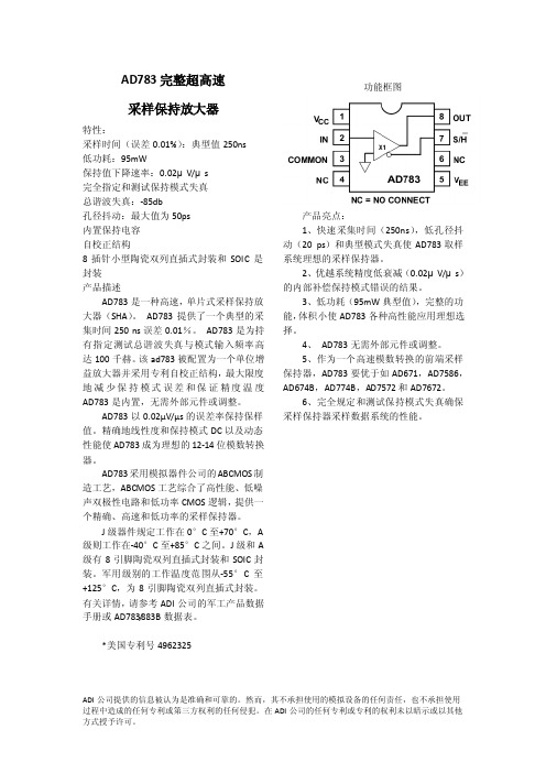
图1所示为一个插入式附件的原理图,它可以配合典型PC声卡采样使用。
每个示波器通道使用一个高速采样保持放大器AD783。
SHA的采样信号由时钟分频器电路的数字输出提供,下文将通过一个例子说明。
AD783输入由一个FET缓冲,因此可以使用简单的交流/直流输入耦合。
在所示的两个通道中,当直流耦合跳线开路且输入为交流耦合时,1 MΩ电阻(R1和R3)提供直流偏置。
采样输出由图中所示的双极点有源RC网络低通滤波。
该滤波器不必是一个有源电路,但所示的滤波器能够提供有益的缓冲低阻抗来驱动PC声卡输入。
图1. 双通道模拟采样电路AD783 SHA提供高达数MHz的可用大信号带宽。
输入端的有效压摆率约为100 V/µs以上。
采用±5 V电源时,输入/输出摆幅至少为±3 V。
对于500 mV p-p以下的摆幅,小信号3 dB带宽接近50 MHz。
利用图1所示的前端电路以及采用Visual Analyser1软件的PC 声卡,可以得到一个以1 MHz频率重复的2 MHz单周期正弦波,如图2的屏幕截图所示。
采样时钟以80.321 kHz的采样速率提供250 ns宽的采样脉冲。
这里的有效水平时基为333 ns/分频比。
例子中使用的PC声卡采用SoundMax®编解码器,其采样速率为96 kSPS。
AD783中文资料
入信号在给定的时间保持命令之间的区别。保
持模式偏移量来自内部开关的电荷注入引入到
保持电容的电压错误。额定保持模式偏移指定
为 0 V 输入条件。AD783 是在-2.5 V 至+2.5 V 的
输出范围也有效的增益误差,非线性保持值,
如在图 2 所示特点。通过 AD783 规格表明,保
持模式偏移量在高温下是非常稳定的。
2.0
V
高电平输入电流(VIN = 5 V) 注释:
2
10
μA
1 指定的并测试超过±2.5 伏的输入电压范围。
规格如有变更,恕不另行通知。
特性
最小值
AD783J/A 典 型值
最大值
单位
电源特性
工作电压范围
±4.75
±5
±5.25
V
供电电流
9.5
17
mA
+电源抑制比(+5V±5%)
45
65
dB
-电源抑制比(-5V±5%)
功能框图
产品亮点: 1、快速 采集时 间(250n s ),低孔 径抖 动(20 ps)和典型模式失真使 AD783 取样 系统理想的采样保持器。 2、优越系统精度低衰减(0.02μ V/μ s) 的内部补偿保持模式错误的结果。 3、低功耗(95mW 典型值),完整的功 能,体积小使 AD783 各种高性能应用理想选 择。 4、 AD783 无需外部元件或调整。 5、作为一个 高速模数 转换的前 端采样 保持器,AD783 要优于如 AD671,AD7586, AD674B,AD774B,AD7572 和 AD7672。 6、完全规定 和测试保 持模式失 真确保 采样保持器采样数据系统的性能。
AD783 是一个完整的,高速采样保持放大 器,可在 250 ns 内提供 12 位精度的高速采样。
TI公司12位ad芯片全

ACTIVE ACTIVE ACTIVE ACTIVE
ADS62P28
ACTIVE
ADS62P25
ACTIVE
12 333kSPS 12 125KSPS 12 125KSPS 12 1MSPS 12 1MSPS 12 125MSPS 12 105MSPS 80MSPS 12 65MSPS 12 12 250MSPS 12 210MSPS 12 125MSPS
SAR
Vref
2
MSP430-ADC12
ACTIVE
Devi ce 12 200kSPS Spec ific
SAR
Vref
2
DELFINO-ADC12 ACTIVE
Devi ce 12 12.5MSP Pipeline Spec S ific 12 730kSPS 12 40kSPS
ACTIVE
12 250kSPS 40kSPS
1
SAR
0.45
ADS8506
ACTIVE
12
1
SAR
0.45
ADS8504
ACTIVE
12 250kSPS 100kSPS 80MSPS 70MSPS 53MSPS 20MSPS
12 5MSPS 10MSPS 25MSPS 12 40MSPS 12 12 12 1MSPS 12 1MSPS 12 1MSPS 12 1MSPS 12 100kSPS 12 1MSPS 12 3MSPS 12 4MSPS 52kSPS 12 12 1MSPS 12 200kSPS 12 2MSPS 12 500kSPS 12 2MSPS
PICCOLO-ADC12 ACTIVE
Devi ce 12 4.6MSPS Spec ific
高速AD芯片集

高位高速AD、DA2010-09-16 13:46:05| 分类:学术专题| 标签:|字号大中小订阅模数转换器(A/D)l 8位分辨率l TLV0831 8 位 49kSPS ADC 串行输出,差动输入,可配置为 SE 输入,单通道l TLC5510 8 位 20MSPS ADC,单通道、内部 S、低功耗l TLC549 8 位、40kSPS ADC,串行输出、低功耗、与 TLC540/545/1540 兼容、单通道l TLC545 8 位、76kSPS ADC,串行输出、片上 20 通道模拟 Mux,19 通道l TLC0831 8 位,31kSPS ADC 串行输出,微处理器外设/独立运算,单通道l TLC0820 8 位,392kSPS ADC 并行输出,微处理器外设,片上跟踪与保持,单通道l ADS931 8 位 30MSPS ADC,具有单端/差动输入和外部基准以及低功耗、电源关闭功能l ADS930 8 位 30MSPS ADC,单端/差动输入具有内部基准以及低功耗、电源关闭功能l ADS830 8 位 60MSPS ADC,具有单端/差动输入、内部基准和可编程输入范围l 10位分辨率l TLV1572 10 位 1.25 MSPS ADC 单通道 DSP/(Q)SPI IF S 极低功耗自动断电功能l TLV1571 1 通道 10 位 1.25MSPS ADC,具有 8 通道输出、DSP/SPI、硬件可配置、低功耗l TLV1549 10 位 38kSPS ADC 串行输出、固有采样功能、终端与 TLC154、 TLC1549x 兼容l TLV1548 10 位 85kSPS ADC 系列输出,可编程供电/断电/转换速率,TMS320 DSP/SPI/QPSI Compat.,8 通道l TLV1544 10 位 85kSPS ADC 串行输出,可编程供电/断电/转换速率,TMS320 DSP/SPI/QPSI 兼容,4 通道l TLV1543 10 位 200 kSPS ADC 串行输出,内置自检测模式,内部 S,引脚兼容。
AD7837ARZ资料

REV. C
Information furnished by Analog Devices is believed to be accurate and reliable. However, no responsibility is assumed by Analog Devices for its use, nor for any infringements of patents or other rights of third parties which may result from its use. No license is granted by implication or otherwise under any patent or patent rights of Analog Devices. One Technology Way, P.O. Box 9106, Norwood, MA 02062-9106, U.S.A. Tel: 781/329-4700 World Wide Web Site: Fax: 781/326-8703 © Analog Devices, Inc., 2000
8/13 ±2 2.4 0.8 ±1 8
8/13 ±2 2.4 0.8 ±1 8
8/13 ±2 2.4 0.8 ±1 8
kΩ min/max % max
V min V max µA max pF max Ω typ mA typ
Digital Inputs at 0 V and VDD
0.2 11
0.2 11
元器件交易网
1 (V = +15 V ؎ 5%, V = –15 V ؎ 5%, AGNDA = AGNDB = DGND AD7837/AD7847–SPECIFICATIONS = O V. V = V = +10 V, R = 2 k⍀, C = 100 pF [V connected to R AD7837]. All specifications T to T unless otherwise noted.)
adc选型表,adc常用型号(A...
adc选型表,adc常用型号(ADC selection form, ADC commonly usedmodel)TI/BB company ADC products:[ADS7812] 1 channels, 12 bit, serial interface, low power, SOIC package;[AMC7820] 8 channels, 12 bit, serial interface, 100kHz sampling rate, TQFP package;[TLC2558] 8 channel, 12 bit, serial interface, 400KSPS, 5V power supply, 0Ref input, SOIC package;[TLV2543] 11 channels, 12 bit, serial interface, low power, DIP package;[TLC2543] 11 channels, 12 bit, serial interface, DIP package;[ADS7869] 12 channels, 12 bit, serial / parallel interface, TQFP package;[TLC3548] 8 channel, 14 bit, serial interface, 200KSPS, 5V power supply, 0Ref input, SOIC package;[ADS8320] 1 channels, 16 bit, serial interface, high speed, 2.7V-5.5V, MSOP package;[ADS8321] 1 channels, 16 bit, serial interface, high speed, MSOP package;[ADS8505] 1 channels, 16 bit, parallel interface, 250-KSPS, SSOP package;[ADS8509] 1 channels, 16 bit, serial interface, 250Ksps, SSOP package;[ADS7809] 1 channels, 16 bit, serial interface, 100Ksps, 5V power supply, SOIC package;[ADS8342] 4 channel, 16 bit parallel interface, 250Ksps, input range -2.52.5, TQFP package;[ADS8345] 8 channels, 16 bit, serial interface, serial, SSOP package;[ADS1241] 4 channels, 24 bit, serial interface, SSOP package;[ADS7835] 1 channels, 24 bit, serial interface, high speed, low power AD converter, MSOP package;AD company ADC products:[AD7864] 4 channels, 12 bit, parallel interface, high-speed simultaneous sampling, single supply, TQFP package;[AD7865] 4 channels, 14 bit, parallel interface, high-speed simultaneous sampling, single supply, TQFP package;[AD677] 1 channels, 16 bit, serial interface, 100KSPS, DIP package;[AD7612] 1 channels, 16 bit, parallel / serial, 750KSPS, single stage / dual stage input, DIP package;[AD7715] 1 channels, 16 bit, serial interface, 3V power supply, DIP package;[AD974] 4 channels, 16 bit, serial interface, single supply, 200KSPS, DIP package;[AD976] 4 channels, 16 bit, serial interface, single supply, 200KSPS, + 10V input, DIP package;[AD7710] 2 channels, 24 bit, serial interface, input programmable gain, SOIC package;MAXIM company ADC products:[MAX156] 4 channels, 8 bit, parallel interface, high speed, voltage reference, DIP package;[MAX158] 8 channels, 8 bit, parallel interface, high speed, voltage reference, DIP package;[MAX160] 1 channel, 8 bit parallel interface, + 5V, + 5, 10 input range, 4 S, DIP package;[MAX176] 1 channels, 12 bit, serial interface, 250ksps, voltage reference, DIP package;[MAX187] 1 channels, 12 bit, serial interface, +5V, low power, DIP package;[MAX163] 1 channels, 12 bit, parallel interface, 5V input, sampling rate 100k, voltage reference, DIP package;[MAX167] 1 channels, 12 bit, parallel interface, + 2.5V input, sampling rate, 100k, voltage reference, DIP package;[MAX144] 2 channels, 12 bit, serial interface, +3V/5V, low power, 108ksps, DIP package;[MAX1282] 4 channels, 12 bit, serial interface, 400ksps, +5V, built in voltage reference, SSOP package;[MAX1270] 8 channels, 12 bit, serial interface, 110ksps, multi range, +5V, built in voltage reference, DIP package;[MAX146] 8 channels, 12 bit, serial interface, +2.7V, low power, DIP package;[MAX186] 8 channels, 12 bit, serial interface, low power, DIP package, SOIC package;[MAX197] 8 channels, 12 bit, parallel interface, multi range, single +5V, DIP package, SOIC package;[MAX110] 2 channels, 14 bit, serial interface, + 3V input, low cost, DIP package;[MAX111] 2 channels, 14 bit, serial interface, + 1.5V input, low cost, DIP package;[MAX1134] 1 channels, 16 bit, serial interface, 150ksps, 3.3V, single power supply, SSOP package;[MAX1165] 1 channels, 16 bit, parallel interface (16 bit), low power, TSSOP package;[MAX1166] 1 channels, 16 bit, parallel interface (8 bit), low power, TSSOP package;[MAX1169] 1 channels, 16 bit, 2 wire serial interface, 58.6ksps, TSSOP package;[MAX7129] 4 1/2 bits, with multiplexed LCD drivers, low-noise, DIP packages.AD7865AS-1 function applications simple description: 14 bit, 4 channel simultaneous sampling, 175KSPS rate analog to digital converter, with 2SHA, and, 2ADCs (industrial level), the original manufacturer is packaged as: PQFPLQFP Function Description: 14 bit 65MSPS analog to digital converter (industrial level) AD6644ASTAD7856AN function applications simple description: 14 bit 8 channel 285KSPS sampling rate analog-to-digital converter (industrial level), the original manufacturer is packaged as: DIPAD537SH Function Description: 150KHZ integrated voltage to frequency converter (military level) TO-99AD537JH function applications simple description: 150KHZ integrated voltage converter (civil level), the original manufacturer is packaged as: TO-99AD75019JP Function Application Description: 16 * 16 audio frequency switch (civil level), the original manufacturer is packaged as: PLCCApplication of AD7701AN Function Description: 16 - Sigma Delta ADC (industrial grade) original manufacturer: DIP packageApplication of AD7705BN Function Description: 16 - Sigma Delta ADC (industrial grade) original manufacturer: DIP packageApplication of AD7706BN Function Description: 16 - Sigma Delta ADC (industrial grade) original manufacturer: DIP packageApplication of AD7715AN-5 Function Description: 16 - Sigma Delta ADC (industrial grade) original manufacturer: DIP 5V power packageApplication of AD7705BR Function Description: 16 - Sigma Delta ADC (industrial grade) original manufacturer: SOIC packageApplication of AD7707BR Function Description: 16 - Sigma Delta ADC (industrial grade) original manufacturer: SOIC packageApplication of AD7715AR-5 Function Description: 16 - Sigma Delta ADC (industrial grade) original manufacturer: SOIC 5V power packageAD1380JD function applications simple description: 16 bit 20us high performance analog to digital converter (civil level)AD1380KD function applications simple description: 16 bit 20us high performance analog to digital converter (civil level)AD569JN Function Description: 16 bit 3us current output digital to analog converter (Civil) DIPAD669AN function application brief description: 16 bit 8us parallel input digital to analog converter (industrial level), the original manufacturer is packaged as: DIPAD660AN function applications simple description: 16 bit 8us serial parallel input, digital to analog converter (industrial level), the original manufacturer is packaged as: DIPAD420AN-32 function applications simple description: 16 bit single power 4-20mA output digital to analog converter (industrial level), the original manufacturer is packaged as: DIPAD420AR-32 function applications simple description: 16 bit single power 4-20mA output digital to analog converter (industrial level), the original manufacturer is packaged as: SOICAD7846JN function description of the application: 16 bit voltage output digital to analog converter (civil level), the original manufacturer is packaged as: DIPAD768AR Function Application Description: 16 bit high-speed current output digital to analog converter (civil level), the original manufacturer is packaged as: SOICAD7660AST function applications simple description: 16 bit 100KSPS CMOS analog to digital converter (industrial level), the original manufacturer is packaged as: LQFPAD676JD function applications simple description: 16 bit 100KSPS sampling rate parallel output ADC (civil level), the original manufacturer is packaged as: DIPAD676JN function applications simple description: 16 bit 100KSPS sampling rate parallel output ADC (civil level), the original manufacturer is packaged as: DIPAD676KD function applications simple description: 16 bit 100KSPS sampling rate parallel output ADC (civil level), the original manufacturer is packaged as: DIPAD677JD function applications simple description: 16 bit 100KSPS sampling rate, serial output analog to digital converter (civil level), the original manufacturer is packaged as: DIPAD677JN function applications simple description: 16 bit 100KSPS sampling rate, serial output analog to digital converter (civil level), the original manufacturer is packaged as: DIP100KSPS sampling rate, serial output analog to digital converter (civil level), the original manufacturer is packaged as: SOICAD7664AST function applications simple description: 16 bit 570KSPS CMOS analog to digital converter (industrial level), the original manufacturer is packaged as: LQFPAD421BN function application brief description: 16 bit loop power supply, in line with the HART agreement, 4-20mA output digital to analog converter (industrial level), the original manufacturer is packaged as: DIPAD421BR function application brief description: 16 bit loop power supply, in line with the HART agreement, 4-20mA output digital to analog converter (industrial level), the original manufacturer is packaged as: SOICAD7506JN function applications simple description: 16 election 1 CMOS multiplexer (civil level), the original manufacturer is packaged as: DIPAD650JN function application brief description: 1MHz, voltage frequency converter (civil level), the original manufacturer is packaged as: DIPAD650KN function application brief description: 1MHz, voltage frequency converter (civil level), the original manufacturer is packaged as: DIPchannel sample and hold amplifier (civil level), the original manufacturer is packaged as: DIPAD780AN function description simple description: 2.5V or 3V optional output high-precision voltage reference source (industrial level), the original manufacturer is packaged as: DIPApplication of AD7703AN Function Description: 20 - Sigma Delta ADC (industrial grade) original manufacturer: DIP packageApplication of AD7703BN Function Description: 20 - Sigma Delta ADC (industrial grade) original manufacturer: DIP packageApplication of AD7710AN Function Description: 24 - Sigma Delta ADC (industrial grade) original manufacturer: DIP packageApplication of AD7711AN Function Description: 24 - Sigma Delta ADC (industrial grade) original manufacturer: DIP packageApplication of AD7713AN Function Description: 24 - Sigma Delta ADC (industrial grade) original manufacturer: DIP packageApplication of AD7731BN Function Description: 24 - Sigma Delta ADC (industrial grade) original manufacturer: DIP packageApplication of AD7712AN Function Description: 24 - Sigma Delta ADC (industrial grade) original manufacturer: DIP packageApplication of AD7714AN-3 Function Description: 24 - SigmaDelta ADC (industrial grade) original manufacturer: DIP 3V power packageApplication of AD7714AN-5 Function Description: 24 - Sigma Delta ADC (industrial grade) original manufacturer: DIP 5V power packageAD652AQ function application brief description: 2MHz, synchronous voltage frequency converter (industrial level), the original manufacturers are packaged as: DIPAD585AQ function application brief description: 3us sample and hold amplifier (industrial level), the original manufacturers are packaged as: DIPAD654JN function application brief description: 500KHz, low price, voltage, frequency converter (civil level), the original manufacturer is packaged as: DIPAD654JR function application brief description: 500KHz, low price, voltage, frequency converter (civil level), the original manufacturer is packaged as: SOIC。
ADS7825

CS PWRD
CDAC
8kΩ
8kΩ
8kΩ CAP
REF
Buffer 6kΩ
Internal +2.5V Ref
Comparator
Serial
Data
Out
or
Parallel
Data
8
Out
BUSY DATACLK SDATA
D7-D0 BYTE
International Airport Industrial Park • Mailing Address: PO Box 11400, Tucson, AZ 85734 • Street Address: 6730 S. Tucson Blvd., Tucson, AZ 85706 • Tel: (520) 746-1111 • Twx: 910-952-1111 Internet: / • FAXLine: (800) 548-6133 (US/Canada Only) • Cable: BBRCORP • Telex: 066-6491 • FAX: (520) 889-1510 • Immediate Product Info: (800) 548-6132
40
T
±3
15
16
0.8
±0.5
±7
±0.5
±2
±10
±2
±0.1±8Fra bibliotek90T
–90
83
86
83
86
100
120
T
2
90
T T T
T T
±2
T ±0.25
±5 ±0.25
T T
T ±0.1 T
T
- 1、下载文档前请自行甄别文档内容的完整性,平台不提供额外的编辑、内容补充、找答案等附加服务。
- 2、"仅部分预览"的文档,不可在线预览部分如存在完整性等问题,可反馈申请退款(可完整预览的文档不适用该条件!)。
- 3、如文档侵犯您的权益,请联系客服反馈,我们会尽快为您处理(人工客服工作时间:9:00-18:30)。
介绍该ads7835是一个12位,采样模数转换器(模数)完成采样(中/小时),内部参考,并同步串行接口。
典型功耗17.5mw在500 kHz吞吐率。
该装置可进入掉电模式,降低功耗只是2.5mw。
输入范围–基准以+,和内部参考可驱动由一个外部电压。
低功耗,体积小,高速度使ads7835理想的电池供电系统随着无线通信设备,便携式多通道数据记录器,和频谱分析仪。
本串行接口也提供了低成本隔离远程数据采集。
SPECIFICATIONS注释:(1)理想的输入范围,不包括收益或偏移误差。
(2),是最重要的一点,与参考电压等于+道,一个是1.22mv。
(3)测量相对理想的积极全面的2.499v积极全面的错误。
衡量相对于理想负全面的–2.499v负尺寸误差。
(4)计算的前九个谐波的输入频率。
(5)如果需要内部参考电流源的外部负载,参考电压将改变由于内部功率电阻器。
(6)可以改变±30%。
此处提供的信息被认为是可靠的;然而,输入错误或遗漏不承担任何责任。
路承担任何责任为这些信息的使用,和所有此类信息的使用应在用户完全自己的风险。
价格和规格如有更改通知。
没有专利权或许可证的任何描述的电路均为暗示或授予任何第三方。
用不授权或保证任何输入产品用于生命支持设备和/或系统。
ABSOLUTE MAXIMUM RATINGS(1)注:(1)强调比列在“绝对最大额定值”对设备造成永久性的损坏。
暴露在绝对最大条件长时间可能会影响设备的可靠性。
ELECTROSTATIC DISCHARGE SENSITIVITY静电放电可能造成的损害从绩效降解完成设备故障。
路公司建议所有集成电路处理和储存使用适当的静电放电保护方法。
损害的范围可以从细微的性能下降完成设备故障。
精密集成电路可能更容易受到损害,因为非常小参数变化可能导致设备不能满足公布的规格。
PIN ASSIGNMENTS参考输出。
分离与地面0.1 m F陶瓷电容器和2.2mf钽电容器。
输入转换。
控制采样/保持模式,开始启动转换,串行数据传输,类型的串行传输,断电模式。
看到数字接口部分获取更多信息。
串行数据输出。
12位串行传输转换的结果是最重要的一点,每个点的第一个有效前沿时钟。
通过适当控制机的输入,这可能是有数据传输的最低有效位第一。
看到的数字接口部分的更多信息。
PACKAGE/ORDERING INFORMATION注:(1)详细图纸尺寸表,请参见数据结束表或包装绘图文件网络。
(2)性能等级信息的特点是在卷筒。
(3)模型以斜线(/)是唯一可在磁带和卷轴数量表示(例如/ 250表示250个单位每卷,表明2500/职业每卷)。
订购2500件“ads7835e/职业”将得到一个单一的2500-piece磁带和卷轴。
详细的磁带和卷轴的机械信息,请参阅网站下的应用和磁带和卷轴定位和尺寸。
(4)信噪比为不指定,典型的只。
然而,没有失踪的时候码是保证在温度。
THEORY OF OPERATIONads7835是高速逐次逼近寄存器(特区)模拟数字转换器(模数)的内部的带隙基准。
该架构是基于电容再分配本身包括一个/小时功能的。
该转换器在0.6米互补金属氧化物半导体过程。
参见图1电路的基本操作ads7835。
该ads7835需要一个外部时钟运行转换过程。
这个时钟可以改变(12.5khz200通量)和8mhz(500 kHz吞吐量)。
工作周期的时钟是不重要的,只要最低高度低倍至少度和时钟周期在至少125ns。
最小的时钟频率,由泄漏的电容器内部的ads7835。
模拟输入的ads7835单端。
本ads7835提供了一个真正的双极输入输入摆在地面。
当使用内部参考输入范围±道(在±20mv为低等级和±模式下的高年级)。
当使用一个外部参考输入范围–+基准参考电压。
本ads7835将接受外部参考范围对2.9v2。
数字转换结果是提供一个串口方式,同步的时钟输入。
提供的结果最重要的是位(最高有效位)第一和代表的结果目前的转换progress-there没有管道延迟。
通过适当控制转换和时钟输入,这是可能获得的数字结果最重要的一点。
ANALOG INPUT模拟输入(引脚2)的ads7835连接到机床机床×电压分配器。
这种分频器允许ads7835接受双极性输入操作时,从一个单一的5供应。
该分压器连接到输出缓冲区的内部+的供应。
当输入是在全面(+道),在输入电压的华助(电容数字模拟转换器)也是+的产生微不足道的输入电流。
当输入是在–全面(–道),在输入电压的华助会是0造成1.25ma电流源出的输入引脚。
这是建议,缓冲区放置模拟之间的输入信号和输入的ads7835。
输入阻抗的ads7835取决于是否该装置是在样品或保持模式。
当取样,输入有一个主输入阻抗的参考。
本源的模拟输入电压必须能够充输入阻抗(通常25pf||千瓦)为12位沉降在同一时期。
这可以尽可能少350ns在一些操作模式。
当转换器是在举行模式,输入阻抗开关约机组地面。
必须注意的是输入电压销。
输入信号应保持在–5.3v和 5.3v(以供)避免损坏转换器。
REFERENCE参考电压的参考电压引脚直接设置全面范围的模拟输入。
ads7835可以操作的与参考范围在2到2.9v,为全面±2到±2.9v范围。
电压的参考电压引脚的内部缓冲和这缓冲区驱动华助部分的转换器。
这是重要因为缓冲大大降低了动力负载放置在参考源。
然而,在电压参考电压将仍然包含一些噪音和故障由特区转换过程。
这些可减少仔细绕过参考电压引脚接地概述部分遵循。
INTERNAL REFERENCEads7835包含一个板上的参考,从而在–道至道输入范围的模拟输入。
本规格表给出了各种规格为内部参考。
这可以用来提供一个参考少量的电流源的外部负载,但负荷应该是静态的。
由于内部功率电阻,一动态负荷会引起变化的参考电压,并将大大影响转换结果。
请注意,即使静态负载将降低内部参考电压在输入缓冲区。
减少的数额取决于载荷及实际价值的“内部化”的电阻。
该电阻值可以通过不同的±30%。
该参考电压引脚应绕过一个0.1 m F电容器放在尽可能的ads7835包。
在此外,一个2.2mf钽电容器应使用在并联陶瓷电容器。
此位置电容器,而不是关键的性能,应放置作为接近尽可能的包。
EXTERNAL REFERENCE内部参考连接到参考电压引脚和所述内部缓冲区通过连续串联电阻。
因此,参考电压可以很容易地驱动由一个外部参考电压。
电压范围的外部电压2到2.9v,相应的模拟输入范围为22.9v两例。
而外部参考源将不重要电流的参考电压引脚,它具有驱动功率串联电阻,终止在道内参考(确切的电阻值会不同了±30%从部分到部分)。
此外,该参考电压引脚应还是绕过地面至少0.1 m F陶瓷电容器(放在靠近的ads7835越好)。
本参考将是稳定的,该电容性负载。
这取决于特定的参考和模数转换速度,可能需要额外的旁路电容,这样如图1所示2.2mf钽电容器。
理由选择一个外部参考的内部参考各不相同,但主要有2个原因。
一种是实现一个给定的输入范围。
另一种是提供更大的稳定温度。
(通常是内部参考20ppm/°,转化成一个全面的漂移大约有一个输出代码为每12°角这不是考虑到其他来源的全面漂移。
)如果更大稳定温度是必要的,然后一个外部参考低温度漂移的需要。
DIGITAL INTERFACE图2显示了串行数据时序图3显示基本转换时间为ads7835。
具体的时间数字列于表一,有几个重要的项目在图3,给转换器的更多典型的8引脚功能转换器。
首先,该从样本模式保持模式同步下降沿转换和不依赖于时钟。
其次,时钟输入不需要是连续的在采样模式。
转换完成后时钟可保持低或高。
异步性质转换时钟提出有趣的可能性,但也有一些设计考虑。
图3显示,方便有时间限制与时钟(tckch和tckcs)。
然而,如果这些时间侵犯(这可能发生如果转换是完全异步时钟),转换器将进行转换正确,但确切时间转换不确定的。
由于建立时间和保持时间之间的转换和时钟已经违反了在这个例子中,开始转换可以由一个时钟周期。
(注意,开始转换可以侦测到使用上拉电阻数据。
当数据下降了高阻抗变低,转换已经开始,时钟周期是第一次的转换。
)此外,如果转换是完全异步时钟和时钟是连续的,有可能将时钟过渡之前可要低。
如果发生这种情况速度比10nstckch表示,有机会一些数字馈可能耦合到举行电容器。
这可能导致一个小偏移误差,特定的转换。
因此,有一个基本的操作方法ads7835。
转换可以是同步的时钟和时钟可以是连续的。
这是典型的情况时,接口转换到一个数字信号处理器。
二方法是在方便的异步时钟和门控时钟的运行(连续时钟)。
这方法是比较典型的一个spi-like接口上单片机。
这种方法也可被允许产生一个触发电路和启动(在一些延迟)开始时钟。
这些方法包括下的接口和串行接口部分这个数据表。
POWER-DOWN TIMING转换时序图3所示的结果不是该ads7835进入省电模式。
如果转换速率的装置高(接近500 kHz),有权力很小,可节省使用省电模式。
然而,由于断电模式不受惩罚的第一转换(转换有效)在较低的采样率,显着的权力可以保存通过允许装置进入省电模式之间转换。
图4显示了典型的方法将模数为在掉电模式。
如果转换是保持在低转换和开始低第十三个时钟周期,该装置进入省电模式。
它仍然在这直到前沿大会注意转换必须高至少tacq以抽样信号正确以及电内部节点。
有不同的方法ads7835时钟。
第一个涉及缩放的时钟输入有关的转换率。
例如,一个8mhz输入时钟和时序图3所示的结果在500 kHz转换率。
同样,一个1.6mhz时钟将导致一个100 kHz转换率。
另一方法包括保持时钟输入接近最大时钟速率的并开始转换需要。
这个时间是类似的图4所示。
作为一个例子,一个50khz转换将需要160个时钟周期,而每次转换在16个时钟周期,用于在500 kHz。
主要的区别是两国之间的时间量该ads7835仍然断电。
在第一种模式,该转换器只停留在断电的一小时钟周期数(取决于多少个时钟期间有每次转换)。
为转换表,转换总是花相同的百分比时间在断电。
由于低功耗的数字逻辑,有一小减少功率消耗,但它是非常轻微的。
这种影响可以看到在典型性能曲线”供应电流与采样率。
”与此相反,另一种方法(时钟在一个固定的速率)是指每一个时钟周期的转换需要。
如之间的转换时间变长,变矩器仍然在断电的比例越来越多的时间。
这减少总功率消耗相当数量。
例如,一个50khz转换率的结果大致1/ 10的功率(减去参考),是用在11ads7835®500 kHz转换率。
LSB-FIRST DATA TIMING图5显示了一个方法来传输数字结果在最低有效位格式。