DS90LV031AWGQML中文资料
DS90CF366中文资料

DS90CF386/DS90CF366+3.3V LVDS Receiver 24-Bit Flat Panel Display (FPD)Link—85MHz,+3.3V LVDS Receiver 18-Bit Flat Panel Display (FPD)Link—85MHzGeneral DescriptionThe DS90CF386receiver converts the four LVDS data streams (Up to 2.38Gbps throughput or 297.5Megabytes/sec bandwidth)back into parallel 28bits of CMOS/TTL data (24bits of RGB and 4bits of Hsync,Vsync,DE and CNTL).Also available is the DS90CF366that converts the three LVDS data streams (Up to 1.78Gbps throughput or 223Megabytes/sec bandwidth)back into parallel 21bits of CMOS/TTL data (18bits of RGB and 3bits of Hsync,Vsync and DE).Both Receivers’outputs are Falling edge strobe.A Rising edge or Falling edge strobe transmitter (DS90C385/DS90C365)will interoperate with a Falling edge strobe Re-ceiver without any translation logic.The DS90CF386is also offered in a 64ball,0.8mm fine pitch ball grid array (FBGA)package which provides a 44%reduction in PCB footprint compared to the 56L TSSOP package.This chipset is an ideal means to solve EMI and cable size problems associated with wide,high speed TTL interfaces.Featuresn 20to 85MHz shift clock supportn Rx power consumption <142mW (typ)@85MHz Grayscalen Rx Power-down mode <1.44mW (max)n ESD rating >7kV (HBM),>700V (EIAJ)n Supports VGA,SVGA,XGA and Single Pixel SXGA.n PLL requires no external componentsn Compatible with TIA/EIA-644LVDS standard n Low profile 56-lead or 48-lead TSSOP packagen DS90CF386also available in a 64ball,0.8mm fine pitch ball grid array (FBGA)packageBlock DiagramsDS90CF386DS90CF36610108527Order Number DS90CF386MTD or DS90CF386SLC See NS Package Number MTD56or SLC64A10108528Order Number DS90CF366MTD See NS Package Number MTD48TRI-STATE ®is a registered trademark of National Semiconductor Corporation.May 2003DS90CF386/DS90CF366+3.3V LVDS Receiver 24-Bit-Color Flat Panel Display (FPD)Link—85MHz,+3.3V LVDS Receiver 18-Bit-Color Flat Panel Display (FPD)Link—85MHz©2003National Semiconductor Corporation Absolute Maximum Ratings(Note 1)If Military/Aerospace specified devices are required,please contact the National Semiconductor Sales Office/Distributors for availability and specifications.Supply Voltage (V CC )−0.3V to +4VCMOS/TTL Output Voltage −0.3V to (V CC +0.3V)LVDS Receiver Input Voltage −0.3V to (V CC +0.3V)Junction Temperature +150˚CStorage Temperature−65˚C to +150˚CLead Temperature(Soldering,4sec for TSSOP)+260˚C Solder Reflow Temperature (Soldering,20sec for FBGA)+220˚CMaximum Package Power Dissipation Capacity @25˚C MTD56(TSSOP)Package:DS90CF386MTD 1.61W MTD48(TSSOP)Package:DS90CF366MTD 1.89W Package Derating:DS90CF386MTD12.4mW/˚C above +25˚CDS90CF366MTD15mW/˚C above +25˚CMaximum Package Power Dissipation Capacity @25˚C SLC64A Package:DS90CF386SLC 2.0WPackage Derating:DS90CF386SLC 10.2mW/˚C above +25˚CESD Rating(HBM,1.5k Ω,100pF)>7kV (EIAJ,0Ω,200pF)>700VRecommended Operating ConditionsMin Nom Max UnitsSupply Voltage (V CC ) 3.03.33.6VOperating Free Air Temperature (T A )−10+25+70˚C Receiver Input Range 02.4V Supply Noise Voltage (V CC )100mV PPElectrical CharacteristicsOver recommended operating supply and temperature ranges unless otherwise specified.Symbol ParameterConditions Min Typ Max Units CMOS/TTL DC SPECIFICATIONSV IH High Level Input Voltage 2.0VCC V V IL Low Level Input Voltage GND0.8V V OH High Level Output Voltage I OH =-0.4mA 2.7 3.3V V OL Low Level Output Voltage I OL =2mA 0.060.3V V CL Input Clamp Voltage I CL =−18mA-0.79-1.5V I IN Input CurrentV IN =0.4V,2.5V or V CC +1.8+15uA V IN =GND -100uA I OS Output Short Circuit Current V OUT =0V -60-120mA LVDS RECEIVER DC SPECIFICATIONSV TH Differential Input High Threshold VCM=+1.2V+100mV V TL Differential Input Low Threshold −100mV I INInput CurrentV IN =+2.4V,V CC =3.6V ±10µA VIN=0V,V CC =3.6V±10µARECEIVER SUPPLY CURRENT ICCRWReceiver Supply Current C L =8pF,f =32.5MHz 4970mA Worst CaseWorst Case Pattern,f =37.5MHz 5375mA DS90CF386(Figures 1,4)f =65MHz 81114mA f =85MHz 96135mA ICCRWReceiver Supply Current C L =8pF,f =32.5MHz 4960mA Worst CaseWorst Case Pattern,f =37.5MHz 5365mA DS90CF366(Figures 1,4)f =65MHz 78100mA f =85MHz 90115mA ICCRGReceiver Supply Current,C L =8pF,f =32.5MHz 2845mA 16Grayscale16Grayscale Pattern,f =37.5MHz3047mAD S 90C F 386/D S 90C F 366 2DS90CF386/DS90CF366 Electrical Characteristics(Continued)Over recommended operating supply and temperature ranges unless otherwise specified.Symbol Parameter Conditions Min Typ Max Units RECEIVER SUPPLY CURRENT(Figures2,3,4)f=65MHz4360mAf=85MHz4370mAICCRZ Receiver Supply Current Power Down=Low140400µA Power Down Receiver Outputs Stay Low duringPower Down ModeNote1:“Absolute Maximum Ratings”are those values beyond which the safety of the device cannot be guaranteed.They are not meant to imply that the device should be operated at these limits.The tables of“Electrical Characteristics”specify conditions for device operation.Note2:Typical values are given for V CC=3.3V and T A=+25C.Note3:Current into device pins is defined as positive.Current out of device pins is defined as negative.Voltages are referenced to ground unless otherwise specified(except V OD and∆V OD).Receiver Switching CharacteristicsOver recommended operating supply and temperature ranges unless otherwise specifiedSymbol Parameter Min Typ Max UnitsCLHT CMOS/TTL Low-to-High Transition Time(Figure4) 2.0 3.5nsCHLT CMOS/TTL High-to-Low Transition Time(Figure4) 1.8 3.5nsf=85MHz0.490.84 1.19nsRSPos0Receiver Input Strobe Position for Bit0(Figure11,Figure12)RSPos1Receiver Input Strobe Position for Bit1 2.17 2.52 2.87nsRSPos2Receiver Input Strobe Position for Bit2 3.85 4.20 4.55nsRSPos3Receiver Input Strobe Position for Bit3 5.53 5.88 6.23nsRSPos4Receiver Input Strobe Position for Bit47.217.567.91nsRSPos5Receiver Input Strobe Position for Bit58.899.249.59nsRSPos6Receiver Input Strobe Position for Bit610.5710.9211.27nsRSKM RxIN Skew Margin(Note4)(Figure13)f=85MHz290psRCOP RxCLK OUT Period(Figure5)11.76T50nsRCOH RxCLK OUT High Time(Figure5)f=85MHz 4.557nsRCOL RxCLK OUT Low Time(Figure5) 4.05 6.5nsRSRC RxOUT Setup to RxCLK OUT(Figure5) 2.0nsRHRC RxOUT Hold to RxCLK OUT(Figure5) 3.5nsRCCD RxCLK IN to RxCLK OUT Delay@25˚C,V CC=3.3V(Figure6) 5.57.09.5nsRPLLS Receiver Phase Lock Loop Set(Figure7)10msRPDD Receiver Power Down Delay(Figure10)1µsNote4:Receiver Skew Margin is defined as the valid data sampling region at the receiver inputs.This margin takes into account the transmitter pulse positions(min and max)and the receiver input setup and hold time(internal data sampling window-RSPos).This margin allows for LVDS interconnect skew,inter-symbol interference(both dependent on type/length of cable),and clock jitter(less than150ps).3AC Timing Diagrams10108502FIGURE 1.“Worst Case”Test Pattern10108512FIGURE 2.“16Grayscale”Test Pattern (DS90CF386)(Notes 5,6,7,8)D S 90C F 386/D S 90C F 366 4AC Timing Diagrams(Continued)Note 5:The worst case test pattern produces a maximum toggling of digital circuits,LVDS I/O and CMOS/TTL I/O.Note 6:The 16grayscale test pattern tests device power consumption for a “typical”LCD display pattern.The test pattern approximates signal switching needed to produce groups of 16vertical stripes across the display.Note 7:Figures 1,3show a falling edge data strobe (TxCLK IN/RxCLK OUT).Note 8:Recommended pin to signal mapping.Customer may choose to define differently.10108503FIGURE 3.“16Grayscale”Test Pattern (DS90CF366)(Notes 5,6,7,8)10108504FIGURE 4.DS90CF386/DS90CF366(Receiver)CMOS/TTL Output Load and Transition Times10108505FIGURE 5.DS90CF386/DS90CF366(Receiver)Setup/Hold and High/Low TimesDS90CF386/DS90CF3665AC Timing Diagrams(Continued)10108506FIGURE 6.DS90CF386/DS90CF366(Receiver)Clock In to Clock Out Delay10108507FIGURE 7.DS90CF386/DS90CF366(Receiver)Phase Lock Loop Set Time10108509FIGURE 8.28Parallel TTL Data Inputs Mapped to LVDS Outputs -DS90CF386D S 90C F 386/D S 90C F 366 6AC Timing Diagrams(Continued)10108510FIGURE 9.21Parallel TTL Data Inputs Mapped to LVDS Outputs -DS90CF36610108508FIGURE 10.DS90CF386/DS90CF366(Receiver)Power Down DelayDS90CF386/DS90CF3667AC Timing Diagrams(Continued)10108525FIGURE 11.DS90CF386(Receiver)LVDS Input Strobe PositionD S 90C F 386/D S 90C F 366 8DS90CF386/DS90CF366 AC Timing Diagrams(Continued)10108526FIGURE12.DS90CF366(Receiver)LVDS Input Strobe Position9AC Timing Diagrams(Continued)10108511C —Setup and Hold Time (Internal data sampling window)defined by Rspos (receiver input strobe position)min and max Tppos —Transmitter output pulse position (min and max)RSKM =Cable Skew (type,length)+Source Clock Jitter (cycle to cycle)(Note 9)+ISI (Inter-symbol interference)(Note 10)Cable Skew —typically 10ps–40ps per foot,media dependent Note 9:Cycle-to-cycle jitter is less than 250ps at 85MHz.Note 10:ISI is dependent on interconnect length;may be zero.FIGURE 13.Receiver LVDS Input Skew MarginD S 90C F 386/D S 90C F 366 10DS90CF386/DS90CF366 DS90CF386MTD56Package Pin Description—24-Bit FPD Link ReceiverPin Name I/O No.DescriptionRxIN+I4Positive LVDS differentiaI data inputs.RxIN−I4Negative LVDS differential data inputs.RxOUT O28TTL level data outputs.This includes:8Red,8Green,8Blue,and3controllines—FPLINE,FPFRAME,DRDY(also referred to as HSYNC,VSYNC,DataEnable).RxCLK IN+I1Positive LVDS differential clock input.RxCLK IN−I1Negative LVDS differential clock input.RxCLK OUT O1TTL Ievel clock output.The falling edge acts as data strobe.PWR DOWN I1TTL level input.When asserted(low input)the receiver outputs are low.V CC I4Power supply pins for TTL outputs.GND I5Ground pins for TTL outputs.PLL V CC I1Power supply for PLL.PLL GND I2Ground pin for PLL.LVDS V CC I1Power supply pin for LVDS inputs.LVDS GND I3Ground pins for LVDS inputs.DS90CF366MTD48Package Pin Description—18-Bit FPD Link ReceiverPin Name I/O No.DescriptionRxIN+I3Positive LVDS differentiaI data inputs.RxIN−I3Negative LVDS differential data inputs.RxOUT O21TTL level data outputs.This includes:6Red,6Green,6Blue,and3control lines—FPLINE,FPFRAME,DRDY(also referred to as HSYNC,VSYNC,Data Enable).RxCLK IN+I1Positive LVDS differential clock input.RxCLK IN−I1Negative LVDS differential clock input.RxCLK OUT O1TTL Ievel clock output.The falling edge acts as data strobe.PWR DOWN I1TTL level input.When asserted(low input)the receiver outputs are low.V CC I4Power supply pins for TTL outputs.GND I5Ground pins for TTL outputs.PLL V CC I1Power supply for PLL.PLL GND I2Ground pin for PLL.LVDS V CC I1Power supply pin for LVDS inputs.LVDS GND I3Ground pins for LVDS inputs.DS90CF386—64ball FBGA package Pin Description—FPD Link ReceiverPin Name I/O No.DescriptionRxIN+I4Positive LVDS differentiaI data inputs.RxIN−I4Negative LVDS differential data inputs.RxOUT O28TTL level data outputs.This includes:8Red,8Green,8Blue,and4control lines—FPLINE,FPFRAME,DRDY(also referred to as HSYNC,VSYNC,Data Enable).RxCLK IN+I1Positive LVDS differential clock input.RxCLK IN−I1Negative LVDS differential clock input.FPSHIFT OUT O1TTL Ievel clock output.The falling edge acts as data strobe.Pin name RxCLK OUT.PWR DOWN I1TTL level input.When asserted(low input)the receiver outputs are low.V CC I4Power supply pins for TTL outputs.GND I5Ground pins for TTL outputs.PLL V CC I1Power supply for PLL.PLL GND I2Ground pin for PLL.LVDS V CC I1Power supply pin for LVDS inputs.11DS90CF386—64ball FBGA package Pin Description —FPD Link Receiver (Continued)Pin Name I/O No.DescriptionLVDS GND I3Ground pins for LVDS inputs.NC6Pins not connected.DS90CF386Pin Description —64ball FBGA Package —FPD Link ReceiverBy PinBy Pin Type Pin Pin Name Type Pin Pin Name TypeA1RxOUT17O A4GND G A2VCC P B1GND G A3RxOUT15O B6GND G A4GND G D8GND G A5RxOUT12O E3GND G A6RxOUT8O E5LVDS GND G A7RxOUT7O G3LVDS GND G A8RxOUT6O G7LVDS GND G B1GND GH5LVDS GND G B2NC F6PLL GND G B3RxOUT16O G8PLL GND G B4RxOUT11O E6PWR DWN I B5VCC P H6RxCLKIN-I B6GND G H7RxCLKIN+I B7RxOUT5O H2RxIN0-I B8RxOUT3O H3RxIN0+I C1RxOUT21O F4RxIN1-I C2NC G4RxIN1+I C3RxOUT18O G5RxIN2-I C4RxOUT14O F5RxIN2+I C5RxOUT9O G6RxIN3-I C6RxOUT4O H8RxIN3+I C7NC E7RxCLKOUT O C8RxOUT1O E8RxOUT0O D1VCC P C8RxOUT1O D2RxOUT20O D5RxOUT10O D3RxOUT19O B4RxOUT11O D4RxOUT13O A5RxOUT12O D5RxOUT10O D4RxOUT13O D6VCC P C4RxOUT14O D7RxOUT2O A3RxOUT15O D8GND G B3RxOUT16O E1RxOUT22O A1RxOUT17O E2RxOUT24O C3RxOUT18O E3GND G D3RxOUT19O E4LVDS VCC P D7RxOUT2O E5LVDS GND G D2RxOUT20O E6PWR DWN I C1RxOUT21O E7RxCLKOUT O E1RxOUT22O E8RxOUT0O F1RxOUT23OD S 90C F 386/D S 90C F 366 12DS90CF386/DS90CF366 DS90CF386Pin Description—64ball FBGA Package—FPD Link Receiver(Continued)By Pin By Pin TypeF1RxOUT23O E2RxOUT24OF2RxOUT26O G1RxOUT25OF3NC F2RxOUT26OF4RxIN1-I H1RxOUT27OF5RxIN2+I B8RxOUT3OF6PLL GND G C6RxOUT4OF7PLL VCC P B7RxOUT5OF8NC A8RxOUT6OG1RxOUT25O A7RxOUT7OG2NC A6RxOUT8OG3LVDS GND G C5RxOUT9OG4RxIN1+I E4LVDS VCC PG5RxIN2-I H4LVDS VCC PG6RxIN3-I F7PLL VCC PG7LVDS GND G A2VCC PG8PLL GND G B5VCC PH1RxOUT27O D1VCC PH2RxIN0-I D6VCC PH3RxIN0+I B2NCH4LVDS VCC P C2NCH5LVDS GND G C7NCH6RxCLKIN-I F3NCH7RxCLKIN+I F8NCH8RxIN3+I G2NCG:GroundI:InputO:OutputP:PowerNC:Not connectted13Pin Diagrams for TSSOP PackagesDS90CF386MTDDS90CF366MTD1010852310108513Applications InformationPOWER SEQUENCING AND POWERDOWN MODEOutputs of the transmitter remain in TRI-STATE until the power supply reaches 2V.Clock and data outputs will begin to toggle 10ms after V CC has reached 3V and the Power-down pin is above 1.5V.Either device may be placed into a powerdown mode at any time by asserting the Powerdown pin (active low).Total power dissipation for each device will decrease to 5µW (typical).The transmitter input clock may be applied prior to powering up and enabling the transmitter.The transmitter input clock may also be applied after power up;however,the use of the PWR DOWN pin is required as described in the Transmitter Input Clock section.Do not power up and enable (PWR DOWN =HIGH)the transmitter without a valid clock signal applied to the TxCLK IN pin.The FPD Link chipset is designed to protect itself from accidental loss of power to either the transmitter or receiver.If power to the transmit board is lost,the receiver clocks (input and output)stop.The data outputs (RxOUT)retain the states they were in when the clocks stopped.When thereceiver board loses power,the receiver inputs are con-trolled by a failsafe bias circuitry.The LVDS inputs are High-Z during initial power on and power off conditions.Current is limited (5mA per input)by the fixed current mode drivers,thus avoiding the potential for latchup when power-ing the device.RECEIVER FAILSAFE FEATUREThe FPD Link receivers have input failsafe bias circuitry to guarantee a stable receiver output for floating or terminated receiver inputs.Under these conditions receiver inputs will be pulled to a HIGH state.This is the case if not all data channels are required in the application.Leave the extra channel’s inputs open.This minimizes power dissipation and locks the unused channels outputs into a stable known (HIGH)state.If a clock signal is present,data outputs will all be HIGH;if the clock input is also floating/terminated,data outputs will remain in the last valid state.A floating/terminated clock input will result in a LOW clock output.D S 90C F 386/D S 90C F 366 14Physical Dimensionsinches (millimeters)unless otherwise noted56-Lead Molded Thin Shrink Small Outline Package,JEDECDimensions shown in millimeters onlyOrder Number DS90CF386MTD NS Package Number MTD5648-Lead Molded Thin Shrink Small Outline Package,JEDECDimensions shown in millimeters onlyOrder Number DS90CF366MTD NS Package Number MTD48DS90CF386/DS90CF36615Physical Dimensionsinches (millimeters)unless otherwise noted (Continued)64ball,0.8mm fine pitch ball grid array (FBGA)PackageDimensions show in millimeters Order Number DS90CF386SLC NS Package Number SLC64ALIFE SUPPORT POLICYNATIONAL’S PRODUCTS ARE NOT AUTHORIZED FOR USE AS CRITICAL COMPONENTS IN LIFE SUPPORT DEVICES OR SYSTEMS WITHOUT THE EXPRESS WRITTEN APPROVAL OF THE PRESIDENT AND GENERAL COUNSEL OF NATIONAL SEMICONDUCTOR CORPORATION.As used herein:1.Life support devices or systems are devices or systems which,(a)are intended for surgical implant into the body,or (b)support or sustain life,and whose failure to perform when properly used in accordance with instructions for use provided in the labeling,can be reasonably expected to result in a significant injury to the user.2.A critical component is any component of a life support device or system whose failure to perform can be reasonably expected to cause the failure of the life support device or system,or to affect its safety or effectiveness.National Semiconductor Americas Customer Support CenterEmail:new.feedback@ Tel:1-800-272-9959National SemiconductorEurope Customer Support CenterFax:+49(0)180-5308586Email:europe.support@Deutsch Tel:+49(0)6995086208English Tel:+44(0)8702402171Français Tel:+33(0)141918790National Semiconductor Asia Pacific Customer Support CenterEmail:ap.support@National SemiconductorJapan Customer Support Center Fax:81-3-5639-7507Email:jpn.feedback@ Tel:81-3-5639-7560D S 90C F 386/D S 90C F 366+3.3V L V D S R e c e i v e r 24-B i t -C o l o r F l a t P a n e l D i s p l a y (F P D )L i n k —85M H z ,+3.3V L V D S R e c e i v e r 18-B i t -C o l o r F l a t P a n e l D i s p l a y (F P D )L i n k —85M H zNational does not assume any responsibility for use of any circuitry described,no circuit patent licenses are implied and National reserves the right at any time without notice to change said circuitry and specifications.。
DS90CR287_04中文资料

DS90CR287/DS90CR288A+3.3V Rising Edge Data Strobe LVDS 28-Bit Channel Link-85MHzGeneral DescriptionThe DS90CR287transmitter converts 28bits of LVCMOS/LVTTL data into four LVDS (Low Voltage Differential Signal-ing)data streams.A phase-locked transmit clock is transmit-ted in parallel with the data streams over a fifth LVDS link.Every cycle of the transmit clock 28bits of input data are sampled and transmitted.The DS90CR288A receiver con-verts the four LVDS data streams back into 28bits of LVCMOS/LVTTL data.At a transmit clock frequency of 85MHz,28bits of TTL data are transmitted at a rate of 595Mbps per LVDS data ing a 85MHz clock,the data throughput is 2.38Gbit/s (297.5Mbytes/sec).This chipset is an ideal means to solve EMI and cable size problems associated with wide,high-speed TTL interfaces.Featuresn 20to 85MHz shift clock supportn 50%duty cycle on receiver output clock n 2.5/0ns Set &Hold Times on TxINPUTs n Low power consumptionn ±1V common-mode range (around +1.2V)n Narrow bus reduces cable size and cost n Up to 2.38Gbps throughputn Up to 297.5Mbytes/sec bandwidthn 345mV (typ)swing LVDS devices for low EMI n PLL requires no external components n Rising edge data stroben Compatible with TIA/EIA-644LVDS standard nLow profile 56-lead TSSOP packageBlock DiagramsDS90CR28710108701Order Number DS90CR287MTD See NS Package Number MTD56DS90CR288A10108727Order Number DS90CR288AMTD See NS Package Number MTD56July 2004DS90CR287/DS90CR288A +3.3V Rising Edge Data Strobe LVDS 28-Bit Channel Link-85MHz©2004National Semiconductor Corporation Pin Diagram for TSSOP PackagesDS90CR287DS90CR288A1010872110108722Typical Application10108723D S 90C R 287/D S 90C R 288A 2Absolute Maximum Ratings(Note1)If Military/Aerospace specified devices are required, please contact the National Semiconductor Sales Office/ Distributors for availability and specifications.Supply Voltage(V CC)−0.3V to+4V CMOS/TTL Input Voltage−0.5V to(V CC+0.3V) CMOS/TTL Output Voltage−0.3V to(V CC+0.3V) LVDS Receiver Input Voltage−0.3V to(V CC+0.3V) LVDS Driver Output Voltage−0.3V to(V CC+0.3V) LVDS Output Short CircuitDuration Continuous Junction Temperature+150˚C Storage Temperature−65˚C to+150˚C Lead Temperature(Soldering,4sec.)+260˚C Solder Reflow TemperatureMaximum Package Power Dissipation@+25˚CMTD56(TSSOP)Package:DS90CR287MTD 1.63WDS90CR288AMTD 1.61WPackage Derating:DS90CR287MTD12.5mW/˚C above+25˚C DS90CR288AMTD12.4mW/˚C above+25˚C ESD Rating(HBM,1.5kΩ,100pF)>7kV (EIAJ,0Ω,200pF)>700V Latch Up Tolerance@+25˚C>±300mA Recommended Operating ConditionsMin Nom Max Units Supply Voltage(V CC) 3.0 3.3 3.6VOperating Free AirTemperature(T A)−10+25+70˚CReceiver Input Range0 2.4VSupply Noise Voltage(V CC)100mV PPElectrical CharacteristicsOver recommended operating supply and temperature ranges unless otherwise specifiedSymbol Parameter Conditions Min Typ Max Units LVCMOS/LVTTL DC SPECIFICATIONSV IH High Level Input Voltage 2.0V CC VV IL Low Level Input Voltage GND0.8VV OH High Level Output Voltage I OH=−0.4mA 2.7 3.3VV OL Low Level Output Voltage I OL=2mA0.060.3VV CL Input Clamp Voltage I CL=−18mA−0.79−1.5VI IN Input Current V IN=0.4V,2.5V or V CC+1.8+15µAV IN=GND−100µAI OS Output Short Circuit Current V OUT=0V−60−120mALVDS DRIVER DC SPECIFICATIONSV OD Differential Output Voltage R L=100Ω250290450mV∆V OD Change in V OD betweenComplimentary Output States35mVV OS Offset Voltage(Note4) 1.125 1.25 1.375V∆V OS Change in V OS betweenComplimentary Output States35mVI OS Output Short Circuit Current V OUT=0V,R L=100Ω−3.5−5mAI OZ Output TRI-STATE Current PWR DWN=0V,V OUT=0V or V CC±1±10µALVDS RECEIVER DC SPECIFICATIONSV TH Differential Input High Threshold V CM=+1.2V+100mVV TL Differential Input Low Threshold−100mVI IN Input Current V IN=+2.4V,V CC=3.6V±10µAV IN=0V,V CC=3.6V±10µADS90CR287/DS90CR288A3Electrical Characteristics(Continued)Over recommended operating supply and temperature ranges unless otherwise specifiedSymbol ParameterConditionsMinTyp Max Units TRANSMITTER SUPPLY CURRENTI CCTWTransmitter Supply Current Worst Case (with Loads)R L =100Ω,C L =5pF,Worst Case Pattern(Figures 1,2)f =33MHz 3145mA f =40MHz 3250mA f =66MHz 3755mA f =85MHz4260mA I CCTZTransmitter Supply Current Power DownPWR DWN =LowDriver Outputs in TRI-STATE under Powerdown Mode 1055µARECEIVER SUPPLY CURRENT I CCRWReceiver Supply Current Worst CaseC L =8pF,Worst Case Pattern(Figures 1,3)f =33MHz 4970mA f =40MHz 5375mA f =66MHz 81114mA f =85MHz96135mA I CCRZReceiver Supply Current Power DownPWR DWN =LowReceiver Outputs Stay Low during Powerdown Mode140400µANote 1:“Absolute Maximum Ratings”are those values beyond which the safety of the device cannot be guaranteed.They are not meant to imply that the device should be operated at these limits.The tables of “Electrical Characteristics”specify conditions for device operation.Note 2:Typical values are given for V CC =3.3V and T A =+25˚C.Note 3:Current into device pins is defined as positive.Current out of device pins is defined as negative.Voltages are referenced to ground unless otherwise specified (except V OD and ∆V OD ).Note 4:V OS previously referred as V CM .Transmitter Switching CharacteristicsOver recommended operating supply and temperature ranges unless otherwise specified Symbol ParameterMinTyp Max Units LLHT LVDS Low-to-High Transition Time (Figure 2)0.75 1.5ns LHLT LVDS High-to-Low Transition Time (Figure 2)0.751.5ns TCIT TxCLK IN Transition Time (Figure 4)1.0 6.0ns TPPos0Transmitter Output Pulse Position for Bit0(Figure 14)f =85MHz−0.2000.20ns TPPos1Transmitter Output Pulse Position for Bit1 1.48 1.68 1.88ns TPPos2Transmitter Output Pulse Position for Bit2 3.16 3.36 3.56ns TPPos3Transmitter Output Pulse Position for Bit3 4.84 5.04 5.24ns TPPos4Transmitter Output Pulse Position for Bit4 6.52 6.72 6.92ns TPPos5Transmitter Output Pulse Position for Bit58.208.408.60ns TPPos6Transmitter Output Pulse Position for Bit69.8810.0810.28ns TCIP TxCLK IN Period (Figure 5)11.76T 50ns TCIH TxCLK IN High Time (Figure 5)0.35T 0.5T 0.65T ns TCIL TxCLK IN Low Time (Figure 5)0.35T 0.5T0.65Tns TSTC TxIN Setup to TxCLK IN (Figure 5)f =85MHz 2.5ns THTC TxIN Hold to TxCLK IN (Figure 5)0ns TCCD TxCLK IN to TxCLK OUT Delay (Figure 7)T A =25˚C,V CC =3.3V 3.86.3ns TPLLS Transmitter Phase Lock Loop Set (Figure 9)10ms TPDD Transmitter Powerdown Delay (Figure 12)100ns TJITTxCLK IN Cycle-to-Cycle Jitter (Input clock requirement)2nsD S 90C R 287/D S 90C R 288A 4DS90CR287/DS90CR288A Receiver Switching CharacteristicsOver recommended operating supply and temperature ranges unless otherwise specifiedSymbol Parameter Min Typ Max UnitsCLHT CMOS/TTL Low-to-High Transition Time(Figure3)2 3.5nsCHLT CMOS/TTL High-to-Low Transition Time(Figure3) 1.8 3.5nsRSPos0Receiver Input Strobe Position for Bit0(Figure15)f=85MHz0.490.84 1.19nsRSPos1Receiver Input Strobe Position for Bit1 2.17 2.52 2.87nsRSPos2Receiver Input Strobe Position for Bit2 3.85 4.20 4.55nsRSPos3Receiver Input Strobe Position for Bit3 5.53 5.88 6.23nsRSPos4Receiver Input Strobe Position for Bit47.217.567.91nsRSPos5Receiver Input Strobe Position for Bit58.899.249.59nsRSPos6Receiver Input Strobe Position for Bit610.5710.9211.27nsRSKM RxIN Skew Margin(Note5)(Figure16)f=85MHz290psRCOP RxCLK OUT Period(Figure6)11.76T50nsRCOH RxCLK OUT High Time(Figure6)f=85MHz45 6.5nsRCOL RxCLK OUT Low Time(Figure6) 3.556nsRSRC RxOUT Setup to RxCLK OUT(Figure6) 3.5nsRHRC RxOUT Hold to RxCLK OUT(Figure6) 3.5nsRCCD RxCLK IN to RxCLK OUT Delay@25˚C,V CC=3.3V(Note6)(Figure8) 5.579.5nsRPLLS Receiver Phase Lock Loop Set(Figure10)10msRPDD Receiver Powerdown Delay(Figure13)1µsNote5:Receiver Skew Margin is defined as the valid data sampling region at the receiver inputs.This margin takes into account the transmitter pulse positions(minand max)and the receiver input setup and hold time(internal data sampling window-RSPOS).This margin allows LVDS interconnect skew,inter-symbol interference(both dependent on type/length of cable),and source clock(less than150ps).Note6:Total latency for the channel link chipset is a function of clock period and gate delays through the transmitter(TCCD)and receiver(RCCD).The total latencyfor the217/287transmitter and218/288A receiver is:(T+TCCD)+(2*T+RCCD),where T=Clock period.AC Timing Diagrams Array10108702FIGURE1.“Worst Case”Test Pattern5AC Timing Diagrams(Continued)1010870310108704FIGURE 2.DS90CR287(Transmitter)LVDS Output Load and Transition Times1010870510108706FIGURE 3.DS90CR288A (Receiver)CMOS/TTL Output Load and Transition Times10108707FIGURE 4.DS90CR287(Transmitter)Input Clock Transition Time10108709FIGURE 5.DS90CR287(Transmitter)Setup/Hold and High/Low TimesD S 90C R 287/D S 90C R 288A 6AC Timing Diagrams(Continued)10108710FIGURE 6.DS90CR288A (Receiver)Setup/Hold and High/Low Times10108711FIGURE 7.DS90CR287(Transmitter)Clock In to Clock Out Delay10108712FIGURE 8.DS90CR288A (Receiver)Clock In to Clock Out Delay10108713FIGURE 9.DS90CR287(Transmitter)Phase Lock Loop Set TimeDS90CR287/DS90CR288A7AC Timing Diagrams(Continued)10108714FIGURE 10.DS90CR288A (Receiver)Phase Lock Loop Set Time10108716FIGURE 11.28Parallel TTL Data Inputs Mapped to LVDS Outputs10108717FIGURE 12.Transmitter Powerdown DelayD S 90C R 287/D S 90C R 288A 8AC Timing Diagrams(Continued)10108718FIGURE 13.Receiver Powerdown Delay10108719FIGURE 14.Transmitter LVDS Output Pulse Position MeasurementDS90CR287/DS90CR288A9AC Timing Diagrams(Continued)10108728FIGURE 15.Receiver LVDS Input Strobe PositionD S 90C R 287/D S 90C R 288A 10AC Timing Diagrams(Continued)DS90CR287MTD56(TSSOP)Package Pin Description —Channel Link TransmitterPin Name I/O No.DescriptionTxIN I 28TTL level input.TxOUT+O 4Positive LVDS differential data output.TxOUT−O 4Negative LVDS differential data output.TxCLK IN I 1TTL level clock input.The rising edge acts as data strobe.Pin name TxCLK IN.See Applications Information section.TxCLK OUT+O 1Positive LVDS differential clock output.TxCLK OUT−O 1Negative LVDS differential clock output.PWR DOWN I 1TTL level input.Assertion (low input)TRI-STATES the outputs,ensuring low current at power down.See Applications Information section.V CC I 4Power supply pins for TTL inputs.GND I 5Ground pins for TTL inputs.PLL V CC I 1Power supply pin for PLL.PLL GND I 2Ground pins for PLL.LVDS V CC I 1Power supply pin for LVDS outputs.LVDS GNDI3Ground pins for LVDS outputs.DS90CR288A MTD56(TSSOP)Package Pin Description —Channel Link ReceiverPin Name I/O No.DescriptionRxIN+I 4Positive LVDS differential data inputs.RxIN−I 4Negative LVDS differential data inputs.RxOUT O 28TTL level data outputs.RxCLK IN+I 1Positive LVDS differential clock input.RxCLK IN−I 1Negative LVDS differential clock input.RxCLK OUT O 1TTL level clock output.The rising edge acts as data strobe.Pin name RxCLK OUT.PWR DOWN I 1TTL level input.When asserted (low input)the receiver outputs are low.V CCI4Power supply pins for TTL outputs.10108720C —Setup and Hold Time (Internal data sampling window)defined by Rspos (receiver input strobe position)min and max Tppos —Transmitter output pulse position (min and max)RSKM ≥Cable Skew (type,length)+Source Clock Jitter (cycle to cycle)(Note 7)+ISI (Inter-symbol interference)(Note 8)Cable Skew —typically 10ps–40ps per foot,media dependent Note 7:Cycle-to-cycle jitter is less than 150ps at 85MHz.Note 8:ISI is dependent on interconnect length;may be zeroFIGURE 16.Receiver LVDS Input Skew MarginDS90CR287/DS90CR288A11DS90CR288A MTD56(TSSOP)Package Pin Description —Channel Link Receiver (Continued)Pin Name I/O No.DescriptionGND I 5Ground pins for TTL outputs.PLL V CC I 1Power supply for PLL.PLL GND I 2Ground pin for PLL.LVDS V CC I 1Power supply pin for LVDS inputs.LVDS GNDI3Ground pins for LVDS inputs.D S 90C R 287/D S 90C R 288A 12Applications InformationThe TSSOP version of the DS90CR287and DS90CR288Aare backward compatible with the existing5V Channel Linktransmitter/receiver pair(DS90CR283,DS90CR284).To up-grade from a5V to a3.3V system the following must beaddressed:1.Change5V power supply to3.3V.Provide this supply tothe V CC,LVDS V CC and PLL V CC.2.Transmitter input and control inputs except3.3V TTL/CMOS levels.They are not5V tolerant.3.The receiver powerdown feature when enabled will lockreceiver output to a logic low.The Channel Link devices are intended to be used in a widevariety of data transmission applications.Depending uponthe application the interconnecting media may vary.Forexample,for lower data rate(clock rate)and shorter cablelengths(<2m),the media electrical performance is less critical.For higher speed/long distance applications the me-dia’s performance becomes more critical.Certain cable con-structions provide tighter skew(matched electrical lengthbetween the conductors and pairs).Additional applicationsinformation can be found in the following National InterfaceApplication Notes:AN=####TopicAN-1041Introduction to Channel LinkAN-1108Channel Link PCB and InterconnectDesign-In GuidelinesAN-806Transmission Line TheoryAN-905Transmission Line Calculations andDifferential ImpedanceAN-916Cable InformationCABLES:A cable interface between the transmitter andreceiver needs to support the differential LVDS pairs.The21-bit CHANNEL LINK chipset(DS90CR217/218A)requiresfour pairs of signal wires and the28-bit CHANNEL LINKchipset(DS90CR287/288A)requires five pairs of signalwires.The ideal cable/connector interface would have aconstant100Ωdifferential impedance throughout the path.Itis also recommended that cable skew remain below140ps(@85MHz clock rate)to maintain a sufficient data samplingwindow at the receiver.In addition to the four or five cable pairs that carry data andclock,it is recommended to provide at least one additionalconductor(or pair)which connects ground between thetransmitter and receiver.This low impedance ground pro-vides a common-mode return path for the two devices.Some of the more commonly used cable types for point-to-point applications include flat ribbon,flex,twisted pair andTwin-Coax.All are available in a variety of configurations andoptions.Flat ribbon cable,flex and twisted pair generallyperform well in short point-to-point applications while Twin-Coax is good for short and long applications.When usingribbon cable,it is recommended to place a ground linebetween each differential pair to act as a barrier to noisecoupling between adjacent pairs.For Twin-Coax cable ap-plications,it is recommended to utilize a shield on eachcable pair.All extended point-to-point applications shouldalso employ an overall shield surrounding all cable pairsregardless of the cable type.This overall shield results inimproved transmission parameters such as faster attainablespeeds,longer distances between transmitter and receiverand reduced problems associated with EMS or EMI.The high-speed transport of LVDS signals has been demon-strated on several types of cables with excellent results.However,the best overall performance has been seen whenusing Twin-Coax cable.Twin-Coax has very low cable skewand EMI due to its construction and double shielding.All ofthe design considerations discussed here and listed in thesupplemental application notes provide the subsystem com-munications designer with many useful guidelines.It is rec-ommended that the designer assess the tradeoffs of eachapplication thoroughly to arrive at a reliable and economicalcable solution.RECEIVER FAILSAFE FEATURE:These receivers haveinput failsafe bias circuitry to guarantee a stable receiveroutput for floating or terminated receiver inputs.Under theseconditions receiver inputs will be in a HIGH state.If a clocksignal is present,data outputs will all be HIGH;if the clockinput is also floating/terminated,data outputs will remain inthe last valid state.A floating/terminated clock input willresult in a HIGH clock output.BOARD LAYOUT:To obtain the maximum benefit from thenoise and EMI reductions of LVDS,attention should be paidto the layout of differential lines.Lines of a differential pairshould always be adjacent to eliminate noise interferencefrom other signals and take full advantage of the noisecanceling of the differential signals.The board designershould also try to maintain equal length on signal traces fora given differential pair.As with any high-speed design,theimpedance discontinuities should be limited(reduce thenumbers of vias and no90degree angles on traces).Anydiscontinuities which do occur on one signal line should bemirrored in the other line of the differential pair.Care shouldbe taken to ensure that the differential trace impedancematch the differential impedance of the selected physicalmedia(this impedance should also match the value of thetermination resistor that is connected across the differentialpair at the receiver’s input).Finally,the location of theCHANNEL LINK TxOUT/RxIN pins should be as close aspossible to the board edge so as to eliminate excessive pcbruns.All of these considerations will limit reflections andcrosstalk which adversely effect high frequency performanceand EMI.INPUTS:The TxIN and control pin inputs are compatiblewith LVTTL and LVCMOS levels.This pins are not5V toler-ant.UNUSED INPUTS:All unused inputs at the TxIN inputs ofthe transmitter may be tied to ground or left no connect.Allunused outputs at the RxOUT outputs of the receiver mustthen be left floating.TERMINATION:Use of current mode drivers requires aterminating resistor across the receiver inputs.The CHAN-NEL LINK chipset will normally require a single100Ωresistorbetween the true and complement lines on each differentialpair of the receiver input.The actual value of the terminationresistor should be selected to match the differential modecharacteristic impedance(90Ωto120Ωtypical)of the cable.Figure17shows an example.No additional pull-up or pull-down resistors are necessary as with some other differentialtechnologies such as PECL.Surface mount resistors arerecommended to avoid the additional inductance that ac-companies leaded resistors.These resistors should beplaced as close as possible to the receiver input pins toreduce stubs and effectively terminate the differential lines.DECOUPLING CAPACITORS:Bypassing capacitors areneeded to reduce the impact of switching noise which couldlimit performance.For a conservative approach threeparallel-connected decoupling capacitors(Multi-Layered Ce-DS90CR287/DS90CR288A13Applications Information(Continued)ramic type in surface mount form factor)between each V CC and the ground plane(s)are recommended.The three ca-pacitor values are 0.1µF,0.01µF and 0.001µF.An example is shown in Figure 18.The designer should employ widetraces for power and ground and ensure each capacitor has its own via to the ground plane.If board space is limiting the number of bypass capacitors,the PLL V CC should receive the most filtering/bypassing.Next would be the LVDS V CC pins and finally the logic V CC pins.CLOCK JITTER:The CHANNEL LINK devices employ a PLL to generate and recover the clock transmitted across the LVDS interface.The width of each bit in the serialized LVDS data stream is one-seventh the clock period.For example,a 85MHz clock has a period of 11.76ns which results in a data bit width of 1.68ns.Differential skew (∆t within one differen-tial pair),interconnect skew (∆t of one differential pair to another)and clock jitter will all reduce the available window for sampling the LVDS serial data streams.Care must be taken to ensure that the clock input to the transmitter be a clean low noise signal.Individual bypassing of each V CC to ground will minimize the noise passed on to the PLL,thus creating a low jitter LVDS clock.These measures provide more margin for channel-to-channel skew and interconnect skew as a part of the overall jitter/skew budget.INPUT CLOCK:The input clock should be present at all times when the part in enabled.If the clock is stopped,the PWR DOWN pin should be asserted to disable the PLL.Once the clock is active again,the part can then be enabled.Do not enable the part without a clock present.COMMON-MODE vs.DIFFERENTIAL MODE NOISE MAR-GIN:The typical signal swing for LVDS is 300mV centered at +1.2V.The CHANNEL LINK receiver supports a 100mV threshold therefore providing approximately 200mV of dif-ferential noise mon-mode protection is of more importance to the system’s operation due to the differentialdata transmission.LVDS supports an input voltage range of Ground to +2.4V.This allows for a ±1.0V shifting of the center point due to ground potential differences and common-mode noise.TRANSMITTER INPUT CLOCK:The transmitter input clock must always be present when the device is enabled (PWR DOWN =HIGH).If the clock is stopped,the PWR DOWN pin must be used to disable the PLL.The PWR DOWN pin must be held low until after the input clock signal has been reap-plied.This will ensure a proper device reset and PLL lock to occur.POWER SEQUENCING AND POWERDOWN MODE:Out-puts of the CHANNEL LINK transmitter remain in TRI-STATE until the power supply reaches 2V.Clock and data outputs will begin to toggle 10ms after V CC has reached 3V and the Powerdown pin is above 1.5V.Either device may be placed into a powerdown mode at any time by asserting the Pow-erdown pin (active low).Total power dissipation for each device will decrease to 5µW (typical).The transmitter input clock may be applied prior to powering up and enabling the transmitter.The transmitter input clock may also be applied after power up;however,the use of the PWR DOWN pin is required as described in the Transmitter10108724FIGURE 17.LVDS Serialized Link Termination10108725FIGURE 18.CHANNEL LINK Decoupling ConfigurationD S 90C R 287/D S 90C R 288A14Applications Information(Continued) Input Clock section.Do not power up and enable(PWR DOWN=HIGH)the transmitter without a valid clock signal applied to the TxCLK IN pin.The CHANNEL LINK chipset is designed to protect itself from accidental loss of power to either the transmitter or receiver.If power to the transmit board is lost,the receiver clocks(input and output)stop.The data outputs(RxOUT) retain the states they were in when the clocks stopped. When the receiver board loses power,the receiver inputs are shorted to V CC through an internal diode.Current is limited (5mA per input)by the fixed current mode drivers,thus avoiding the potential for latchup when powering the device.10108726FIGURE19.Single-Ended and Differential WaveformsDS90CR287/DS90CR288A15Physical Dimensionsinches (millimeters)unless otherwise noted56-Lead Molded Thin Shrink Small outline Package,JEDECOrder Number DS90CR287MTD or DS90CR288AMTDDimensions shown in millimeters onlyNS Package Number MTD56LIFE SUPPORT POLICYNATIONAL’S PRODUCTS ARE NOT AUTHORIZED FOR USE AS CRITICAL COMPONENTS IN LIFE SUPPORT DEVICES OR SYSTEMS WITHOUT THE EXPRESS WRITTEN APPROVAL OF THE PRESIDENT AND GENERAL COUNSEL OF NATIONAL SEMICONDUCTOR CORPORATION.As used herein:1.Life support devices or systems are devices or systems which,(a)are intended for surgical implant into the body,or (b)support or sustain life,and whose failure to perform when properly used in accordance with instructions for use provided in the labeling,can be reasonably expected to result in a significant injury to the user. 2.A critical component is any component of a life support device or system whose failure to perform can be reasonably expected to cause the failure of the life support device or system,or to affect its safety or effectiveness.BANNED SUBSTANCE COMPLIANCENational Semiconductor certifies that the products and packing materials meet the provisions of the Customer Products Stewardship Specification (CSP-9-111C2)and the Banned Substances and Materials of Interest Specification (CSP-9-111S2)and contain no ‘‘Banned Substances’’as defined in CSP-9-111S2.National Semiconductor Americas Customer Support CenterEmail:new.feedback@ Tel:1-800-272-9959National SemiconductorEurope Customer Support CenterFax:+49(0)180-5308586Email:europe.support@Deutsch Tel:+49(0)6995086208English Tel:+44(0)8702402171Français Tel:+33(0)141918790National Semiconductor Asia Pacific Customer Support CenterEmail:ap.support@National SemiconductorJapan Customer Support Center Fax:81-3-5639-7507Email:jpn.feedback@ Tel:81-3-5639-7560D S 90C R 287/D S 90C R 288A +3.3V R i s i n gE d g e D a t a S t r o b e L V D S 28-B i t C h a n n e l L i n k -85M H zNational does not assume any responsibility for use of any circuitry described,no circuit patent licenses are implied and National reserves the right at any time without notice to change said circuitry and specifications.。
HDW-031中文资料

2 screw locks and HDW-029 retainer screws Screw lock kit includes
2 screw locks and
HDW-043A screws retainer Slide lock post set includes 2 posts, HDW-043A washers and lock-washers Slide lock post set
Thread Depth .100 [2.54] Min
#4-40 X .15 DP Inside Thread .188 [4.78] Across Flats
#4-40 X .15 DP Inside Thread .188 [4.78] Across Flats
PART NUMBER JS-01
Slide lock assembly kit includes slide lock, HDW-043-XX screws and washers, Slide lock assembly kit Specify 9, 15, 25 or includes slide lock, 37 position screws and washers,
元器件交易网
D-SUBMINIATURE
Adam Technologies, Inc. Jackscrews
Thread Depth .100 [2.54] Min
HARDWARE & ACCESSORIES
HDW SERIES
JACKSCREW DIMENSIONS
Jackscrews
A .416 [10.60]
S-90N0312SMA-TF资料

4
Seiko Instruments Inc.
Rev.3.0_00 Typical Characteristics
N-CHANNEL POWER MOS FET FOR SWITCHING S-90N0312SMA
DRAIN CURRENT vs. DRAIN TO SOURCE VOLTAGE Pulse test (600 µs), Ta = 25°C
Conditions
Table 4
Item Symbol
Input capacitance Output capacitance Feedback capacitance
Ciss Coss Crss
(Ta = 25°C unless otherwise specified) Min. Typ. Max. Conditions Unit pF 170 VDS = 10 V, VGS = 0 V, f = 1 MHz 55 40
Item Symbol Conditions Mounted on a ceramics board 2 (1225 mm × 1 mm)
(Ta = 25°C unless otherwise specified) Min. Typ. Max. Unisistance (Channel to ambience)
Drain cut-off current Gate to source leakage current Gate to source cut-off voltage *1 Drain to source on-state resistance
Forward transfer admittance Body drain diode forward voltage *1. Effective during pulse test (600 µs). Dynamic characteristics
DS92LV1212A中文资料

DS92LV1212A16-40MHz 10-Bit Bus LVDS Random Lock Deserializer with Embedded Clock RecoveryGeneral DescriptionThe DS92LV1212A is an upgrade of the DS92LV1212.It maintains all of the features of the DS92LV1212.The DS92LV1212A is designed to be used with the DS92LV1021Bus LVDS Serializer.The DS92LV1212A receives a Bus LVDS serial data stream and transforms it into a 10-bit wide parallel data bus and separate clock.The reduced cable,PCB trace count and connector size saves cost and makes PCB layout easier.Clock-to-data and data-to-data skews are eliminated since one input receives both clock and data bits serially.The powerdown pin is used to save power by reduc-ing the supply current when the device is not in use.The Deserializer will establish lock to a synchronization pattern within specified lock times but it can also lock to a data stream without SYNC patterns.Featuresn Clock recovery without SYNC patterns-random lock n Guaranteed transition every data transfer cyclen Chipset (Tx +Rx)power consumption <300mW (typ)@40MHzn Single differential pair eliminates multi-channel skew n 400Mbps serial Bus LVDS bandwidth (at 40MHz clock)n 10-bit parallel interface for 1byte data plus 2control bits or UTOPIA I Interfacen Synchronization mode and LOCK indicator n Flow-through pinout for easy PCB layoutn High impedance on receiver inputs when power is off n Programmable edge trigger on clock n Footprint compatible with DS92LV1210n Small 28-lead SSOP package-MSABlock DiagramTRI-STATE ®is a registered trademark of National Semiconductor Corporation.DS101387-1November 2000DS92LV1212A 16-40MHz 10-Bit Bus LVDS Random Lock Deserializer with Embedded Clock Recovery©2000National Semiconductor Corporation Block Diagram(Continued)Functional DescriptionThe DS92LV1212is a 10-bit Deserializer chip designed to receive data over heavily loaded differential backplanes at clock speeds from 16MHz to 40MHz.It may also be used to receive data over Unshielded Twisted Pair (UTP)cable.The chip has three active states of operation:Initialization,Data Transfer,and Resynchronization;and two passive states:Powerdown and TRI-STATE ®.The following sections describe each operation of the active and passive states.InitializationBefore data can be transferred,the Deserializer must be initialized.The Deserializer should be powered up with the PWRDN pin held low.After V CC stabilizes,the PWRDN pin can be forced high.The Deserializer is ready to lock to the incoming data stream.Step 1:When you apply V CC to the Deserializer,the respec-tive outputs are held in TRI-STATE and internal circuitry is disabled by on-chip power-on circuitry.When V CC reaches V CC OK (2.5V),the PLL is ready to lock to incoming data or synchronization patterns.You must apply the local clock to the REFCLK pin.The Deserializer LOCK output will remain high while its PLL locks to incoming data or to SYNC patterns on the inputs.Step 2:The Deserializer PLL must synchronize to the Seri-alizer to complete the initialization.The Deserializer will lock to non-repetitive data patterns;however,the transmission of SYNC patterns to the Deserializer enables the Deserializer to lock to the Serializer signal within a specified time.See Figure 7.The user’s application determines control of the SYNC1and SYNC2pins.One recommendation is a direct feedback loop from the LOCK pin.Under all circumstances,the Serializer stops sending SYNC patterns after both SYNC inputs return low.When the Deserializer detects edge transitions at the Bus LVDS input,it will attempt to lock to the embedded clock information.When the Deserializer locks to the Bus LVDS clock,the LOCK output will go low.When LOCK is low,the Deserializer outputs represent incoming Bus LVDS data.Data TransferAfter initialization,the Serializer will accept data from inputs DIN0–DIN9.The Serializer uses the TCLK input to latch incoming Data.The TCLK_R/F pin selects which edge the Serializer uses to strobe incoming data.TCLK_R/F high selects the rising edge for clocking data and low selects the falling edge.If either of the SYNC inputs is high for 5*TCLK cycles,the data at DIN0-DIN9is ignored regardless of clock edge.After determining which clock edge to use,a start and stop bit,appended internally,frame the data bits in the register.The start bit is always high and the stop bit is always low.The start and stop bits function as the embedded clock bits in the serial stream.Serialized data and clock bits (10+2bits)are received at 12times the TCLK frequency.For example,if TCLK is 40MHz,the serial rate is 40x 12=480Mega bits per second.Since only 10bits are from input data,the serial “payload”rate is 10times the TCLK frequency.For instance,if TCLK =40MHz,the payload data rate is 40x 10=400Mbps.TCLK is provided by the data source and must be in the range 16MHz to 40MHz nominal.The LOCK pin on the Deserializer is driven low when it is synchronized with the Serializer.The Deserializer locks to the embedded clock and uses it to recover the serialized data.ROUT data is valid when LOCK is low.Otherwise,ROUT0–ROUT9is invalid.The ROUT0-ROUT9pins use the RCLK pin as the reference to data.The polarity of the RCLK edge is controlled by the RCLK_R/F input.See Figure 5.ROUT(0-9),LOCK and RCLK outputs will drive a minimum of three CMOS input gates (15pF load)with 40MHz clock.ResynchronizationWhen the Deserializer PLL locks to the embedded clock edge,the Deserializer LOCK pin asserts a low.If the Dese-rializer loses lock,the LOCK pin output will go high and the outputs (including RCLK)will enter TRI-STATE.The user’s system monitors the LOCK pin to detect a loss of synchronization.Upon detection,the system can arrange to pulse the Serializer SYNC1or SYNC2pin to resynchronize.Multiple resynchronization approaches are possible.OneApplicationDS101387-2D S 92L V 1212A2Resynchronization(Continued) recommendation is to provide a feedback loop using the LOCK pin itself to control the sync request of the Serializer (SYNC1or SYNC2).Dual SYNC pins are provided for mul-tiple control in a multi-drop application.Sending sync pat-terns for resynchronization is desirable when lock times within a specific time are critical.However,the Deserializer can lock to random data,which is discussed in the next section.Random Lock Initialization and ResynchronizationThe initialization and resynchronization methods described in their respective sections are the fastest ways to establish the link between the Serializer and Deserializer.However, the DS92LV1212A can attain lock to a data stream without requiring the Serializer to send special SYNC patterns.This allows the DS92LV1212A to operate in“open-loop”applica-tions.Equally important is the Deserializer’s ability to support hot insertion into a running backplane.In the open loop or hot insertion case,we assume the data stream is essentially random.Therefore,because lock time varies due to data stream characteristics,we cannot possibly predict exact lock time.The primary constraint on“random”lock time is the initial phase relation between the incoming data and the REFCLK when the Deserializer powers up.As described in the next paragraph,the data contained in the data stream can also affect lock time.If a specific pattern is repetitive,the Deserializer could enter “false lock”-falsely recognizing the data pattern as the clocking bits.We refer to such a pattern as a repetitive multi-transition,RMT.This occurs when more than one Low-High transition takes place in a clock cycle over multiple cycles.This occurs when any bit,except DIN9,is held at a low state and the adjacent bit is held high,creating a0-1 transition.In the worst case,the Deserializer could become locked to the data pattern rather than the clock.Circuitry within the DS92LV1212A can detect that the possibility of “false lock”exists.The circuitry accomplishes this by detect-ing more than one potential position for clocking bits.Upon detection,the circuitry will prevent the LOCK output from becoming active until the potential“false lock”pattern changes.The false lock detect circuitry expects the data will eventually change,causing the Deserializer to lose lock to the data pattern and then continue searching for clock bits in the serial data stream.Graphical representations of RMT are shown on the following page.Please note that RMT only applies to bits DIN0-DIN8.PowerdownWhen no data transfer occurs,you can use the Powerdownstate.The Serializer and Deserializer use the Powerdownstate,a low power sleep mode,to reduce power consump-tion.The Deserializer enters Powerdown when you drivePWRDN and REN low.The Serializer enters Powerdownwhen you drive PWRDN low.In Powerdown,the PLL stopsand the outputs enterTRI-STATE,which disables load cur-rent and reduces supply current to the milliampere range.Toexit Powerdown,you must drive the PWRDN pin high.Before valid data exchanges between the Serializer andDeserializer,you must reinitialize and resynchronize the de-vices to each other.Initialization of the Serializer takes510TCLK cycles.The Deserializer will initialize and assert LOCKhigh until lock to the Bus LVDS clock occurs.TRI-STATEThe Serializer enters TRI-STATE when the DEN pin is drivenlow.This puts both driver output pins(DO+and DO−)intoTRI-STATE.When you drive DEN high,the Serializer returnsto the previous state,as long as all other control pins remainstatic(SYNC1,SYNC2,PWRDN,TCLK_R/F).When you drive the REN pin low,the Deserializer entersTRI-STATE.Consequently,the receiver output pins(ROUT0–ROUT9)and RCLK will enter TRI-STATE.TheLOCK output remains active,reflecting the state of the PLL.DS92LV1212A3RMT PatternsOrder NumbersNSIDFunction Package DS92LV1021TMSA Serializer MSA28DS92LV1212AMSADeserializerMSA28DS101387-23DIN0Held Low-DIN1Held High Creates an RMT Pattern DS101387-24DIN4Held Low-DIN5Held High Creates an RMT PatternDS101387-25DIN8Held Low-DIN9Held High Creates an RMT PatternD S 92L V 1212A 4Absolute Maximum Ratings(Note1)If Military/Aerospace specified devices are required, please contact the National Semiconductor Sales Office/ Distributors for availability and specifications.Supply Voltage(V CC)−0.3V to+4V CMOS/TTL Input Voltage−0.3V to(V CC+0.3V) CMOS/TTL Output Voltage−0.3V to(V CC+0.3V) Bus LVDS Receiver InputVoltage−0.3V to+3.9V Junction Temperature+150˚C Storage Temperature−65˚C to+150˚C Lead Temperature(Soldering,4seconds)+260˚C Maximum Package Power Dissipation Capacity@25˚C Package:28L SSOP 1.27W Package Derating:28L SSOP10.3mW/˚C above+25˚C ESD Rating(HBM)>2kVRecommended Operating ConditionsMin Nom Max Units Supply Voltage(V CC) 3.0 3.3 3.6V Operating Free AirTemperature(T A)−40+25+85˚C Receiver Input Range0 2.4V Supply Noise Voltage(V CC)100mV P-PElectrical CharacteristicsOver recommended operating supply and temperature ranges unless otherwise specified.Symbol Parameter Conditions Min Typ Max Units DESERIALIZER LVCMOS/LVTTL DC SPECIFICATIONS(apply to pins PWRDN,RCLK_R/F,REN,REFCLK=inputs;apply to pins ROUT,RCLK,LOCK=outputs)V IH High Level Input Voltage 2.0V CC VV IL Low Level Input Voltage GND0.8VV CL Input Clamp Voltage I CL=−18mA−0.62−1.5VI IN Input Current V IN=0V or3.6V−10±2+15µA V OH High Level Output Voltage I OH=−9mA 2.1 2.93V CC VV OL Low Level Output Voltage I OL=9mA GND0.330.5VI OS Output Short Circuit Current VOUT=0V−15−38−85mA I OZ TRI-STATE Output Current PWRDN or REN=0.8V,V OUT=0V or VCC−10±0.4+10µA DESERIALIZER Bus LVDS DC SPECIFICATIONS(apply to pins RI+and RI−)VTH Differential Threshold HighVoltage VCM=+1.1V+6+50mVVTL Differential Threshold LowVoltage−50−12mV I IN Input Current V IN=+2.4V,V CC=3.6V or0V−10±1+15µAV IN=0V,V CC=3.6V or0V−10±0.05+10µA DESERIALIZER SUPPLY CURRENT(apply to pins DVCC and AVCC)I CCR Deserializer Supply Current C L=15pF f=40MHz5875mAWorst Case Figure1f=16MHz3045mAI CCXR Deserializer Supply CurrentPowerdown PWRDN=0.8V,REN=0.8V0.36 1.0mADeserializer Timing Requirements for REFCLKOver recommended operating supply and temperature ranges unless otherwise specified.Symbol Parameter Conditions Min Typ Max Unitst RFCP REFCLK Period25T62.5nst RFDC REFCLK Duty Cycle50%f Ref REFCLK Frequency0.95/t RCP t RCP 1.05/t RCPt RFTT REFCLK Transition Time36nsDS92LV1212A5Deserializer Switching CharacteristicsOver recommended operating supply and temperature ranges unless otherwise specified.Symbol ParameterConditionsPin/Freq.Min TypMax Units t RCP Receiver out Clock PeriodFigure 3t RCP =t TCP RCLK 2562.5ns t CLH CMOS/TTL Low-to-High Transition Time CL =15pF Figure 2Rout(0-9), 1.24ns t CHL CMOS/TTL High-to-Low Transition Time LOCK,RCLK1.14ns t DDDeserializer DelayFigure 4All Temp./All Freq. 1.75*t RCP +1.25 1.75*t RCP +3.75 1.75*t RCP +6.25nsRoom Temp 3.3V/40MHz1.75*t RCP +2.25 1.75*t RCP +3.75 1.75*t RCP +5.25t ROS ROUT (0-9)Setup Data to RCLKFigure 5RCLK0.4*t RCP 0.5*t RCP ns t ROH ROUT (0-9)Hold Data to RCLK−0.4*t RCP−0.5*t RCPns t RDC RCLK Duty Cycle455055%t HZR HIGH to TRI-STATE Delay Figure 6Rout(0-9),LOCK4.2+0.5*t RCP 10+t RCP ns t LZR LOW to TRI-STATE Delay 4.5+0.5*t RCP 10+t RCP ns t ZHR TRI-STATE to HIGH Delay 6+0.5*t RCP 12+t RCP ns t ZLR TRI-STATE to LOW Delay6.0+0.5*t RCP12+t RCPns t DSR1Deserializer PLL Lock Time from PWRDWN (with SYNCPAT)Figure 7Figure 8(Note 4)16MHz 410µs 40MHz 1.313µs t DSR2Deserializer PLL Lock timefrom SYNCPAT16MHz 1.25µs 40MHz 0.471µs t ZHLK TRI-STATE to HIGH Delay (Power-up)LOCK4.6212ns t RNMDeserializer Noise MarginFigure 9(Note 5)16MHz 9001100ps 40MHz450730psNote 1:“Absolute Maximum Ratings”are those values beyond which the safety of the device cannot be guaranteed.They are not meant to imply that the devices should be operated at these limits.The table of “Electrical Characteristics”specifies conditions of device operation.Note 2:Typical values are given for V CC =3.3V and T A =+25˚C.Note 3:Current into device pins is defined as positive.Current out of device pins is defined as negative.Voltages are referenced to ground except VOD,∆VOD,VTH and VTL which are differential voltages.Note 4:For the purpose of specifying Deserializer PLL performance tDSR1and tDSR2are specified with the REFCLK running and stable,and specific conditions of the incoming data stream (SYNCPATs).It is recommended that the Deserializer be initialized using either tDSR1timing or tDSR2timing.tDSR1is the time required for the Deserializer to indicate lock upon power-up or when leaving the power-down mode.Synchronization patterns should be sent to the device before initiating either condition.tDSR2is the time required to indicate lock for the powered-up and enabled Deserializer when the input (RI+and RI-)conditions change from not receiving data to receiving synchronization patterns (SYNCPATs).Note 5:tRNM is a measure of how much phase noise (jitter)the Deserializer can tolerate in the incoming data stream before bit errors occur.D S 92L V 1212A 6AC Timing Diagrams and Test CircuitsDS101387-4FIGURE 1.“Worst Case”Deserializer ICC Test PatternDS101387-6FIGURE 2.Deserializer CMOS/TTL Output Load and Transition TimesDS101387-11FIGURE 3.Serializer DelayDS101387-12FIGURE 4.Deserializer DelayDS92LV1212A7AC Timing Diagrams and Test Circuits(Continued)DS101387-13Timing shown for RCLK_R/F =LOW Duty Cycle (t RDC )=FIGURE 5.Deserializer Setup and Hold TimesDS101387-14FIGURE 6.Deserializer TRI-STATE Test Circuit and TimingD S 92L V 1212A 8AC Timing Diagrams and Test Circuits(Continued)DS101387-15FIGURE 7.Deserializer PLL Lock Times and PWRDN TRI-STATE DelaysDS101387-22FIGURE 8.Deserializer PLL Lock Time from SyncPATDS92LV1212A9AC Timing Diagrams and Test Circuits(Continued)Application InformationUsing the DS92LV1021and DS92LV1212AThe Serializer and Deserializer chipset is an easy to use transmitter and receiver pair that sends 10bits of parallel LVTTL data over a serial Bus LVDS link up to 660Mbps.An on-board PLL serializes the input data and embeds two clock bits within the data stream.The Deserializer uses a separate reference clock (REFCLK)and an onboard PLL to extract the clock information from the incoming data stream and then deserialize the data.The Deserializer monitors the incoming clock information,determines lock status,and as-serts the LOCK output high when loss of lock occurs.Power ConsiderationsAn all CMOS design of the Serializer and Deserializer makes them inherently low power devices.In addition,the constant current source nature of the Bus LVDS outputs minimizes the slope of the speed vs.I CC curve of conventional CMOS designs.Powering Up the DeserializerThe DS92LV1212A can be powered up at any time by fol-lowing the proper sequence.The REFCLK input can be running before the Deserializer powers up,and it must be running in order for the Deserializer to lock to incoming data.The Deserializer outputs will remain in TRI-STATE until the Deserializer detects data transmission at its inputs and locks to the incoming data stream.Transmitting DataOnce you power up the Serializer and Deserializer,they must be phase locked to each other to transmit data.Phase locking occurs when the Deserializer locks to incoming data or when the Serializer sends patterns.The Serializer sends SYNC patterns whenever the SYNC1or SYNC2inputs are high.The LOCK output of the Deserializer remains high until it has locked to the incoming data stream.Connecting the LOCK output of the Deserializer to one of the SYNC inputs of the Serializer will guarantee that enough SYNC patterns are sent to achieve Deserializer lock.The Deserializer can also lock to incoming data by simply powering up the device and allowing the “random lock”circuitry to find and lock to the data stream.While the Deserializer LOCK output is low,data at the De-serializer outputs (ROUT0-9)is valid,except for the specific case of loss of lock during transmission which is further discussed in the ’Recovering from LOCK Loss’section be-low.Noise MarginThe Deserializer noise margin is the amount of input jitter (phase noise)that the Deserializer can tolerate and still reliably receive data.Various environmental and systematic factors include:Serializer:TCLK jitter,V CC noise (noise bandwidth and out-of-band noise)Media:ISI,Large V CM shifts Deserializer:V CC noiseRecovering from LOCK LossIn the case where the Deserializer loses lock during data transmission,up to 3cycles of data that were previously received can be invalid.This is due to the delay in the lock detection circuit.The lock detect circuit requires that invalid clock information be received 4times in a row to indicate loss of lock.Since clock information has been lost,it is possible that data was also lost during these cycles.There-fore,after the Deserializer relocks to the incoming data stream and the Deserializer LOCK pin goes low,at least three previous data cycles should be suspect for bit errors.The Deserializer can relock to the incoming data stream by making the Serializer resend SYNC patterns,as described above,or by random locking,which can take more time,depending on the data patterns being received.Hot InsertionAll the BLVDS devices are hot pluggable if you follow a few rules.When inserting,ensure the Ground pin(s)makes con-tact first,then the VCC pin(s),and then the I/O pins.When removing,the I/O pins should be unplugged first,then the VCC,then the Ground.Random lock hot insertion is illus-trated in Figure 10.PCB ConsiderationsThe Bus LVDS Serializer and Deserializer should be placed as close to the edge connector as possible.In multiple Deserializer applications,the distance from the Deserializer to the slot connector appears as a stub to the Serializer driving the backplane traces.Longer stubs lower the imped-ance of the bus,increase the load on the Serializer,and lower the threshold margin at the Deserializers.Deserializer devices should be placed much less than one inch from slot connectors.Because transition times are very fast on the Serializer Bus LVDS outputs,reducing stub lengths as much as possible is the best method to ensure signal integrity.Transmission MediaThe Serializer and Deserializer can also be used in point-to-point configuration of a backplane,through a PCB trace,or through twisted pair cable.In point-to-point configu-ration,the transmission media need only be terminated atDS101387-21SW -Setup and Hold Time (Internal data sampling window)t JIT -Serializer Output Bit Position Jitter t RSM =Receiver Sampling Margin TimeFIGURE 9.Receiver Bus LVDS Input Skew MarginD S 92L V 1212A10Application Information(Continued)the receiver end.Please note that in point-to-point configu-ration,the potential of offsetting the ground levels of the Serializer vs.the Deserializer must be considered.Also,Bus LVDS provides a +/− 1.2V common mode range at the receiver inputs.Failsafe Biasing for the DS92LV1212AThe DS92LV1212A has an improved input threshold sensi-tivity of +/−50mV versus +/−100mV for the DS92LV1210or DS92LV1212.This allows for greater differential noise mar-gin in the DS92LV1212A.However,in cases where the receiver input is not being actively driven,the increased sensitivity of the DS92LV1212A can pickup noise as a signal and cause unintentional locking .For example,this can occur when the input cable is disconnected.External resistors can be added to the receiver circuit board to prevent noise pick-up.Typically,the non-inverting receiver input is pulled up and the inverting receiver input is pulled down by high value resistors.the pull-up and pull-down resistors (R 1and R 2)provide a current path through the termination resistor (R L )which biases the receiver inputs when they are not connected to an active driver.The value of the pull-up and pull-down resistors should be chosen so that enough current is drawn to provide a +15mV drop across the termination resistor.Please see Figure 11for the Failsafe Biasing Setup.Using t DJIT and t RNM to Validate Signal QualityThe parameters t DJIT and t RNM can be used to generate an eye pattern mask to validate signal quality in an actual application or in simulation.The parameter t DJIT measures the transmitter’s ability to place data bits in the ideal position to be sampled by the receiver.The typical t DJIT parameter of −80pS indicates that the crossing point of the Tx data is 80pS ahead of the ideal crossing point.The t DJIT(min)and t DJIT(max)parameters specify the earliest and latest,repectively,time that a cross-ing will occur relative to the ideal position.The parameter t RNM is calculated by first measuring how much of the ideal bit the receiver needs to ensure correct sampling.After determining this amount,what remains of the ideal bit that is available for external sources of noise is called t RNM .It is the offset from t DJIT(min or max)for the test mask within the eye opening.The vertical limits of the mask are determined by the DS92LV1212A receiver input threshold of +/−50mV.Please refer to the eye mask pattern of Figure 12for a graphic representation of t DJIT and t RNM .DS101387-26The DS92LV1212A can be “Hot Inserted”into operating serial busses without interrupting bus communication.The random lock feature allows the DS92LV1212A to synchronize to the bus traffic and receive data.FIGURE 10.Random Lock Allows Hot Insertion into Serial BussesDS101387-27FIGURE 11.Failsafe Biasing SetupDS92LV1212A11Application Information(Continued)DS101387-28Note:For the DS92LV1021,t DJIT (max)=70pS and t DJIT (min)=−300pSFIGURE ing t DJIT and t RNM to Generate an Eye Pattern Mask and Validate SIgnal QualityD S 92L V 1212A 12Pin DiagramDeserializer Pin DescriptionPin NameI/O No.DescriptionROUT O 15–19,24–28Data Output.±9mA CMOS level outputs.RCLK_R/FI2Recovered Clock Rising/Falling strobe select.TTL level input.Selects RCLK active edge for strobing of ROUT data.High selects rising edge.Low selects falling edge.RI+I 5+Serial Data Input.Non-inverting Bus LVDS differential input.RI−I 6−Serial Data Input.Inverting Bus LVDS differential input.PWRDN I 7Powerdown.TTL level input.PWRDN driven low shuts down the PLL.LOCKO10LOCK goes low when the Deserializer PLL locks onto the embedded clock edge.CMOS level output.Totem pole output structure,does not directly support wire OR connection.RCLK O 9Recovered Clock.Parallel data rate clock recovered from embedded ed to strobe ROUT,CMOS level output.REN I 8Output Enable.TTL level input.TRI-STATEs ROUT0–ROUT9,LOCK and RCLK when driven low.DVCC I 21,23Digital Circuit power supply.DGND I 14,20,22Digital Circuit ground.AVCC I 4,11Analog power supply (PLL and Analog Circuits).AGND I 1,12,13Analog ground (PLL and Analog Circuits).REFCLKI3Use this pin to supply a REFCLK signal for the internal PLL frequency.DS92LV1212AMSA -DeserializerDS101387-19DS92LV1212A13Truth TableINPUTSOUTPUTSPWRDNREN ROUT [0:9]LOCK RCLK H H Z H Z H H Active L Active L X Z Z Z HLZActiveZ1)LOCK Active indicates the LOCK output will reflect the state of the Deserializer with regard to the selected data stream.2)RCLK Active indicates the RCLK will be running if the Deserializer is locked.The Timing of RCLK with respect to ROUT is determined by RCLK_R/F.3)ROUT and RCLK are TRI-STATED when LOCK is asserted High.D S 92L V 1212A 14Physical Dimensionsinches (millimeters)unless otherwise notedLIFE SUPPORT POLICYNATIONAL’S PRODUCTS ARE NOT AUTHORIZED FOR USE AS CRITICAL COMPONENTS IN LIFE SUPPORT DEVICES OR SYSTEMS WITHOUT THE EXPRESS WRITTEN APPROVAL OF THE PRESIDENT AND GENERAL COUNSEL OF NATIONAL SEMICONDUCTOR CORPORATION.As used herein:1.Life support devices or systems are devices or systems which,(a)are intended for surgical implant into the body,or (b)support or sustain life,and whose failure to perform when properly used in accordance with instructions for use provided in the labeling,can be reasonably expected to result in a significant injury to the user.2.A critical component is any component of a life support device or system whose failure to perform can be reasonably expected to cause the failure of the life support device or system,or to affect its safety or effectiveness.National Semiconductor Corporation AmericasTel:1-800-272-9959Fax:1-800-737-7018Email:support@National Semiconductor EuropeFax:+49(0)180-5308586Email:europe.support@Deutsch Tel:+49(0)6995086208English Tel:+44(0)8702402171Français Tel:+33(0)141918790National Semiconductor Asia Pacific Customer Response Group Tel:65-2544466Fax:65-2504466Email:ap.support@National Semiconductor Japan Ltd.Tel:81-3-5639-7560Fax:81-3-5639-7507Note:Package Dimensions are in millimeters only.Order Number DS92LV1212AMSA NS Package Number MSA28DS92LV1212A 16-40MHz 10-Bit Bus LVDS Random Lock Deserializer with Embedded Clock RecoveryNational does not assume any responsibility for use of any circuitry described,no circuit patent licenses are implied and National reserves the right at any time without notice to change said circuitry and specifications.。
DS90C402中文资料

DS90C402Dual Low Voltage Differential Signaling (LVDS)ReceiverGeneral DescriptionThe DS90C402is a dual receiver device optimized for high data rate and low power applications.This device along with the DS90C401provides a pair chip solution for a dual high speed point-to-point interface.The device is in a PCB space saving 8lead small outline package.The receiver offers ±100mV threshold sensitivity,in addition to common-mode noise protection.Featuresn Ultra Low Power Dissipation n Operates above 155.5Mbps n Standard TIA/EIA-644n 8Lead SOIC Package saves PCB space n V CM ±1V center around 1.2V n±100mV Receiver SensitivityConnection DiagramFunctional DiagramTRI-STATE ®is a registered trademark of National Semiconductor Corporation.DS100006-1Order Number DS90C402M See NS Package Number M08ADS100006-2June 1998DS90C402Dual Low Voltage Differential Signaling (LVDS)Receiver©1998National Semiconductor Corporation Absolute Maximum Ratings(Note1)If Military/Aerospace specified devices are required, please contact the National Semiconductor Sales Office/ Distributors for availability and specifications.Supply Voltage(V CC)−0.3V to+6V Input Voltage(R IN+,R IN−)−0.3V to(V CC+0.3V) Output Voltage(R OUT)−0.3V to(V CC+0.3V) Maximum Package Power Dissipation@+25˚CM Package1025mW Derate M Package8.2mW/˚C above+25˚C Storage Temperature Range−65˚C to+150˚C Lead Temperature RangeSoldering(4sec.)+260˚C Maximum Junction Temperature+150˚C ESD Rating(Note4)(HBM,1.5kΩ,100pF)≥3,500V (EIAJ,0Ω,200pF)≥250VRecommended Operating ConditionsMin Typ Max Units Supply Voltage(V CC)+4.5+5.0+5.5V Receiver Input Voltage GND 2.4V Operating Free AirTemperature(T A)−40+25+85˚CElectrical CharacteristicsOver Supply Voltage and Operating Temperature ranges,unless otherwise specified.(Note2)Symbol Parameter Conditions Pin Min Typ Max UnitsV TH Differential Input High Threshold V CM=+1.2V R IN+,R IN−+100mVV TL Differential Input Low Threshold−100mV I IN Input Current V IN=+2.4V V CC=5.5V−10±1+10µAV IN=0V−10±1+10µA V OH Output High Voltage I OH=−0.4mA,V ID=+200mV R OUT 3.8 4.9VI OH=−0.4mA,Inputs terminated 3.8 4.9VI OH=−0.4mA,Inputs Open 3.8 4.9VI OH=−0.4mA,Inputs Shorted 4.9V V OL Output Low Voltage I OL=2mA,V ID=−200mV0.070.3V I OS Output Short Circuit Current V OUT=0V(Note8)−15−60−100mA I CC No Load Supply Current Inputs Open V CC 3.510mASwitching CharacteristicsV CC=+5.0V±10%,T A=−40˚C to+85˚C(Notes3,4,5,6,9)Symbol Parameter Conditions Min Typ Max Unitst PHLD Differential Propagation Delay High to Low C L=5pF,V ID=200mV(Figure1and Figure2)1.0 3.40 6.0nst PLHD Differential Propagation Delay Low to High 1.0 3.48 6.0ns t SKD Differential Skew|t PHLD−t PLHD|00.08 1.2ns t SK1Channel-to-Channel Skew(Note5)00.6 1.5ns t SK2Chip to Chip Skew(Note6) 5.0ns t TLH Rise Time0.5 2.5ns t THL Fall Time0.5 2.5ns2Parameter Measurement InformationTypical ApplicationApplications InformationLVDS drivers and receivers are intended to be primarily used in an uncomplicated point-to-point configuration as is shown in Figure 3.This configuration provides a clean signaling en-vironment for the quick edge rates of the drivers.The re-ceiver is connected to the driver through a balanced media which may be a standard twisted pair cable,a parallel pair cable,or simply PCB traces.Typically the characteristic im-pedance of the media is in the range of 100Ω.A termination resistor of 100Ωshould be selected to match the media,and is located as close to the receiver input pins as possible.The termination resistor converts the current sourced by the driver into a voltage that is detected by the receiver.Other configurations are possible such as a multi-receiver configu-ration,but the effects of a mid-stream connector(s),cable stub(s),and other impedance discontinuities as well as ground shifting,noise margin limits,and total termination loading must be taken into account.The DS90C402differential line receiver is capable of detect-ing signals as low as 100mV,over a ±1V common-mode range centered around +1.2V.This is related to the driver off-set voltage which is typically +1.2V.The driven signal is cen-tered around this voltage and may shift ±1V around this cen-ter point.The ±1V shifting may be the result of a ground potential difference between the driver’s ground reference and the receiver’s ground reference,the common-mode ef-fects of coupled noise,or a combination of the two.Both re-ceiver input pins should honor their specified operating input voltage range of 0V to +2.4V (measured from each pin to ground),exceeding these limits may turn on the ESD protec-tion circuitry which will clamp the bus voltages.Fail-Safe Feature:The LVDS receiver is a high gain,high speed device that amplifies a small differential signal (20mV)to CMOS logic levels.Due to the high gain and tight threshold of the re-ceiver,care should be taken to prevent noise from appearing as a valid signal.The receiver’s internal fail-safe circuitry is designed to source/sink a small amount of current,providing fail-safe protection (a stable known state HIGH output voltage)for floating,terminated or shorted receiver inputs.1.Open Input Pins.The DS90C402is a dual receiver de-vice,and if an application requires only one receiver,the unused channel(s)inputs should be left OPEN.Do not tie unused receiver inputs to ground or any other volt-ages.The input is biased by internal high value pull up and pull down resistors to set the output to a HIGH state.This internal circuitry will guarantee a HIGH,stable out-put state for open inputs.DS100006-4FIGURE 1.Receiver Propagation Delay and Transition Time Test CircuitDS100006-5FIGURE 2.Receiver Propagation Delay and Transition Time WaveformsDS100006-8FIGURE 3.Point-to-Point Application3Applications Information(Continued)2.Terminated Input.If the driver is disconnected(cableunplugged),or if the driver is in a power-off condition, the receiver output will again be in a HIGH state,even with the end of cable100Ωtermination resistor across the input pins.The unplugged cable can become a float-ing antenna which can pick up noise.If the cable picks up more than10mV of differential noise,the receiver may see the noise as a valid signal and switch.To insure that any noise is seen as common-mode and not differ-ential,a balanced interconnect should be used.Twisted pair cable will offer better balance than flat ribbon cable 3.Shorted Inputs.If a fault condition occurs that shortsthe receiver inputs together,thus resulting in a0V differ-ential input voltage,the receiver output will remain in a HIGH state.Shorted input fail-safe is not supported across the common-mode range of the device(GND to2.4V).It is only supported with inputs shorted and no ex-ternal common-mode voltage applied.Pin DescriptionsPinNo.Name Description 2,6R OUT Receiver output pin3,7R IN+Positive receiver input pin 4,8R IN-Negative receiver input pin 5GND Ground pin1V CC Positive power supply pin,+5V±10%4Ordering InformationOperating Temperature Package Type/NumberOrder Number−40˚C to+85˚C SOP/M08A DS90C402M RECEIVE MODER IN+−R IN−R OUT>+100mV H<−100mV L100mV>&>−100mV XH=Logic High LevelL=Logic Low levelX=Indeterminant StateNote1:“Absolute Maximum Ratings”are those values beyond which the safety of the device cannot be guaranteed.They are not meant to imply that the devices should be operated at these limits.The table of“Electrical Characteristics”specifies conditions of device operation.Note2:Current into device pins is defined as positive.Current out of device pins is defined as negative.All voltages are referenced to ground unless otherwise speci-fied.Note3:All typicals are given for:V CC=+5.0V,T A=+25˚C.Note4:Generator waveform for all tests unless otherwise specified:f=1MHz,Z O=50Ω,t r and t f(0%–100%)≤1ns for R IN.Note5:Channel-to-Channel Skew is defined as the difference between the propagation delay of one channel and that of the others on the same chip with an event on the inputs.Note6:Chip to Chip Skew is defined as the difference between the minimum and maximum specified differential propagation delays.Note7:ESD Rating:HBM(1.5kΩ,100pF)≥3,500VEIAJ(0Ω,200pF)≥250VNote8:Output short circuit current(I OS)is specified as magnitude only,minus sign indicates direction only.Only one output should be shorted at a time,do not ex-ceed maximum junction temperature specification.Note9:C L includes probe and jig capacitance.Typical Performance CharacteristicsOutput High Voltage vsPower Supply VoltageDS100006-9Output High Voltage vsAmbient TemperatureDS100006-10 5Typical Performance Characteristics(Continued)Output Low Voltage vs Power Supply VoltageDS100006-11Output Low Voltage vs Ambient TemperatureDS100006-12Output Short Circuit Current vs Power Supply Voltage DS100006-13Output Short Circuit Current vs Ambient TemperatureDS100006-14Differential Propagation Delay vs Power Supply Voltage DS100006-15Differential Propagation Delay vs Ambient TemperatureDS100006-16 6Typical Performance Characteristics(Continued)Differential Skew vsPower Supply VoltageDS100006-17Differential Skew vsAmbient TemperatureDS100006-18Transition Time vsPower Supply VoltageDS100006-19Transition Time vsAmbient TemperatureDS100006-20 7Physical Dimensions inches(millimeters)unless otherwise notedLIFE SUPPORT POLICYNATIONAL’S PRODUCTS ARE NOT AUTHORIZED FOR USE AS CRITICAL COMPONENTS IN LIFE SUPPORT DE-VICES OR SYSTEMS WITHOUT THE EXPRESS WRITTEN APPROVAL OF THE PRESIDENT OF NATIONAL SEMI-CONDUCTOR CORPORATION.As used herein:1.Life support devices or systems are devices or sys-tems which,(a)are intended for surgical implant intothe body,or(b)support or sustain life,and whose fail-ure to perform when properly used in accordancewith instructions for use provided in the labeling,canbe reasonably expected to result in a significant injuryto the user.2.A critical component in any component of a life supportdevice or system whose failure to perform can be rea-sonably expected to cause the failure of the life supportdevice or system,or to affect its safety or effectiveness.National SemiconductorCorporationAmericasTel:1-800-272-9959Fax:1-800-737-7018Email:support@National SemiconductorEuropeFax:+49(0)180-5308586Email:europe.support@Deutsch Tel:+49(0)180-5308585English Tel:+49(0)180-5327832Français Tel:+49(0)180-5329358Italiano Tel:+49(0)180-5341680National SemiconductorAsia Pacific CustomerResponse GroupTel:65-2544466Fax:65-2504466Email:sea.support@National SemiconductorJapan Ltd.Tel:81-3-5620-6175Fax:81-3-5620-61798-Lead(0.150"Wide)Molded Small Outline Package,JEDECOrder Number DS90C402MNS Package Number M08ADS9C42DualLowVoltageDifferentialSignaling(LVDS)ReceiverNational does not assume any responsibility for use of any circuitry described,no circuit patent licenses are implied and National reserves the right at any time without notice to change said circuitry and specifications.。
DS90LV019TM

August 2000
DS90LV019 3.3V or 5V LVDS Driver/Receiver
General Description
The DS90LV019 is a Driver/Receiver designed specifically for the high speed low power point-to-point interconnect applications. The device operates from a single 3.3V or 5.0V power supply and includes one differential line driver and one receiver. The DS90LV019 features an independent driver and receiver with TTL/CMOS compatibility (DIN and ROUT). The logic interface provides maximum flexibility as 4 separate lines are provided (DIN, DE, RE, and ROUT). The device also features a flow-through pin out which allows easy PCB routing for short stubs between its pins and the connector. The driver has 3.5 mA output loop current.
7.7mW/˚C 790 mW
6.3mW/˚C −65˚C to +150˚C
DS90C385AMTX中文资料
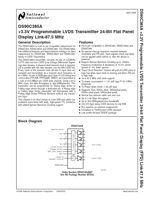
µA
31
45
mA
37
50
mA
48
60
mA
55
65
mA
2
DS90C385A
元器件交易网
Electrical Characteristics (Continued)
Over recommended operating supply and temperature ranges unless otherwise specified.
Duration
Continuous
Junction Temperature
+150˚C
Storage Temperature
−65˚C to +150˚C
Lead Temperature
(Soldering, 4 sec)
+260˚C
Maximum Package Power Dissipation Capacity @ 25˚C
f = 25 MHz f = 40 MHz f = 65 MHz f = 87.5 MHz
Min Typ Max Units
2.0
VCC
V
0
0.8
V
−0.79 −1.5
V
+1.8 +10
µA
−10
0
µA
250 345 450
mV
35
mV
1.13 1.25 1.38
V
35
mV
−3.5 −5
mA
±1 ±10
Block Diagram
DS90C385A
Order Number DS90C385AMT See NS Package Number MTD56
- 1、下载文档前请自行甄别文档内容的完整性,平台不提供额外的编辑、内容补充、找答案等附加服务。
- 2、"仅部分预览"的文档,不可在线预览部分如存在完整性等问题,可反馈申请退款(可完整预览的文档不适用该条件!)。
- 3、如文档侵犯您的权益,请联系客服反馈,我们会尽快为您处理(人工客服工作时间:9:00-18:30)。
Industry Part Number
DS90LV031A
NS Part Numbers
DS90LV031AW-MLS DS90LV031AW-QML DS90LV031AWGMLS DS90LV031AWGQML
Prime Die
DS90LV031A
Controlling Document
SEE FEATURES SECTION
Vos DVos
RL = 100 Ohms RL = 100 Ohms
Dout-, Dout+ Dout-, Dout+
1.125
1.625 50
V mV
1, 2, 3 1, 2, 3
Voh Vol Vih Vil IIH IIL Vcl Ios Ioff Ioz Icc
RL = 100 Ohms RL = 100 Ohms 1 1
2
元器件交易网
MNDS90LV031A-X REV 1C0
MICROCIRCUIT DATA SHEET
(Absolute Maximum Ratings)
(Note 1) Supply Voltage (Vcc) -0.3 to +4V Input Voltage (Din) -0.3 to (Vcc+0.3V) Enable Input Voltage (EN, EN*) -0.3 to (Vcc+0.3V) Output Voltage (Dout+, Dout-) -0.3 to +3.9V Storage Temperature Range -65C to +150C Lead Temperature Soldering (4 sec) 260C ESD Rating. 6000 Volts. Maximum Junction Temperature +150C Maximum Power Dissipation @ +25C (Note 2) 16 PIN CERPAK (W Pkg) 16 PIN CERAMIC SOIC (WG Pkg) Thermal Resistance. (Theta JA) 16 PIN CERPAK (W Pkg) 16 PIN CERAMIC SOIC (WG Pkg) Thermal Resistance. (Theta JC) 16 PIN CERPAK (W Pkg) 16 PIN CERAMIC SOIC (WG Pkg) Note 1:
845mW 845mW 148C/W 148C/W 22C/W 22C/W
Note 2:
Absolute Maximum Ratings are those values beyond which the safety of the device cannot be guaranteed. They are not meant to imply that the device should be operated at these limits. The table of "Electrical Characteristics" provides conditions for actual device operation. Derate (W & WG Pkgs) at 6.8mW/C for temperatures above +25C.
3V LVDS Quad CMOS Differential Line Driver
General Description
The DS90LV031A is a quad CMOS differential line driver utilizing Low Voltage Differentional Signaling (LVDS) technology. It is designed for applications requiring low power dissipation and high data rates. The DS90LV031A accepts TTL/CMOS input levels and translates them to low voltage (350 mV) differential output siginals. In addition the driver supports a TRI-STATE function that may be used to disable the output stage, disabling the load current, and thus dropping the device to a low idle power state. The EN and EN* inputs allow active Low or active High control of the TRI-STATE outputs. The enables are common to all four drivers. The DS90LV031A and companion line receiver (DS90LV032A) provide a new alternative to high power pseudo-ECL devices for high speed point-to-point interface applications. In addition, the DS90LV031A provides power-off high impedance LVDS outputs. This feature assures minimal loading effect on the LVDS bus lines when VCC is not present.
元器件交易网
MICROCIRCUIT DATA SHEET MNDS90LV031A-X REV 1C0
Original Creation Date: 02/09/99 Last Update Date: 08/15/03 Last Major Revision Date: 02/21/00
Processing
MIL-STD-883, Method 5004
Subgrp Description
1 2 3 4 5 6 7 8A 8B 9 10 11 Static tests at Static tests at Static tests at Dynamic tests at Dynamic tests at Dynamic tests at Functional tests at Functional tests at Functional tests at Switching tests at Switching tests at Switching tests at
MICROCIRCUIT DATA SHEET
Features
High impedance LVDS outputs with power-off 3.3V power supply design +/- 350mV differential signaling Low power dissipation. Low differential skew. Low propagation delay Interoperable with existing 5V LVDS devices Military operating temprature range Pin compatible with DS26C31. Compatible with IEEE 1596.3 SCI LVDS standard Compatible with proposed TIA/EIA-644 LVDS standard Typical Rise/Fall times of 800pS. Typical Tri-State Enable/Disable Delays of less than 5nS. CONTROLLING DOCUMENT: DS90LV031AW-QML 5962-9865101QFA DS90LV031AWGQML 5962-9865101QXA
Dout-, Dout+ Dout-, Dout+ .9
1.85
V V
1, 2, 3 1, 2, 3 1, 2, 3 1, 2, 3 1, 2, 3 1, 2, 3 1, 2, 3 1, 2, 3 1, 2, 3 1, 2, 3 1, 2, 3 1, 2, 3 1, 2, 3
Din, 2.0 EN, EN* Din, Gnd EN, EN* Din, EN, EN* Din, EN, EN* Din, EN, EN* Dout-, Dout+ Dout-, Dout+ Dout-, Dout+ Vcc
Temp ( oC)
+25 +125 -55 +25 +125 -55 +25 +125 -55 +25 +125 -55
ቤተ መጻሕፍቲ ባይዱ
Quality Conformance Inspection
MIL-STD-883, Method 5005
1
元器件交易网
MNDS90LV031A-X REV 1C0
Recommended Operating Conditions
Supply Voltage 3.0 to 3.6V Operating Free Air Temperature -55 to +125 C
3
元器件交易网
MNDS90LV031A-X REV 1C0
MICROCIRCUIT DATA SHEET
Electrical Characteristics
DC PARAMETERS