AON5820;中文规格书,Datasheet资料
BTR-5820-SPG中文资料
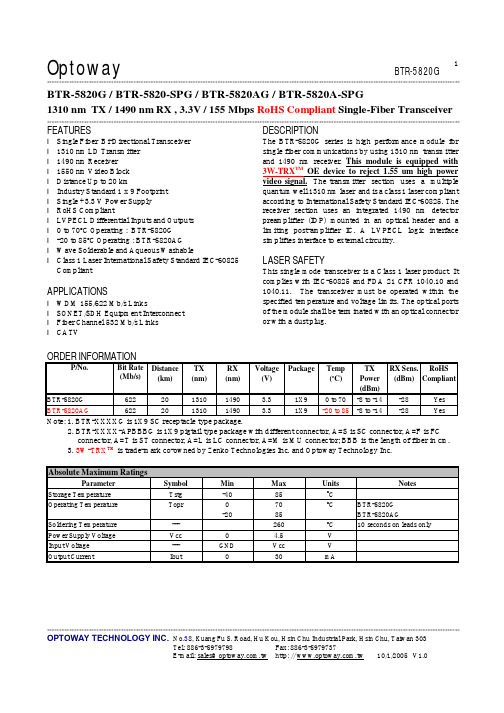
OptowayBTR-5820G**********************************************************************************************************************************************************************************************************************************************************************************************************************************************OPTOWAY TECHNOLOGY INC. No .38, Kuang Fu S. Road, Hu Kou, Hsin Chu Industrial Park, Hsin Chu, Taiwan 3031BTR-5820G / BTR-5820-SPG / BTR-5820AG / BTR-5820A-SPG1310 nm TX / 1490 nm RX , 3.3V / 155 Mbps RoHS Compliant Single-Fiber Transceiver***********************************************************************************************************************************************************************FEATURESl Single Fiber Bi-Directional Transceiver l 1310 nm LD Transmitter l 1490 nm Receiver l 1550 nm Video Block l Distance Up to 20 kml Industry Standard 1 x 9 Footprint l Single +3.3 V Power Supply l RoHS Compliantl LVPECL Differential Inputs and Outputs l 0 to 70o C Operating : BTR-5820G l -20 to 85o C Operating : BTR-5820AG l Wave Solderable and Aqueous Washablel Class 1 Laser International Safety Standard IEC-60825 CompliantAPPLICATIONSl WDM 155/622 Mb/s Linksl SONET/SDH Equipment Interconnect l Fiber Channel 532 Mb/s Links l CATVDESCRIPTIONThe BTR-5820G series is high performance module for single fiber communications by using 1310 nm transmitter and 1490 nm receiver. This module is equipped with 3W-TRX TM OE device to reject 1.55 um high power video signal. The transmitter section uses a multiple quantum well 1310 nm laser and is a class 1 laser compliant according to International Safety Standard IEC-60825. The receiver section uses an integrated 1490 nm detector preamplifier (IDP) mounted in an optical header and a limiting post-amplifier IC. A LVPECL logic interface simplifies interface to external circuitry.LASER SAFETYThis single mode transceiver is a Class 1 laser product. It complies with IEC-60825 and FDA 21 CFR 1040.10 and 1040.11. The transceiver must be operated within the specified temperature and voltage limits. The optical ports of the module shall be terminated with an optical connector or with a dust plug.ORDER INFORMATIONP/No.Bit Rate (Mb/s) Distance (km) TX (nm) RX (nm) Voltage (V) Package Temp (o C)TX Power (dBm)RX Sens. (dBm) RoHS Compliant BTR-5820G 622 20 1310 1490 3.3 1X9 0 to 70 -8 to -14 -28 Yes BTR-5820AG62220131014903.31X9-20 to 85 -8 to -14 -28 Yes Note: 1. BTR-XXXXG is 1X9 SC receptacle type package.2. BTR-XXXX-APBBBG is 1X9 pigtail type package with different connector, A=S is SC connector, A=F is FCconnector, A=T is ST connector, A=L is LC connector, A=M is MU connector; BBB is the length of fiber in cm.3. 3W-TRX TM is trade-mark co-owned by Zenko Technologies Inc. and Optoway Technology Inc.Absolute Maximum RatingsParameterSymbol Min Max Units NotesStorage Temperature Tstg -40 85 o COperating Temperature Topr 0 -20 70 85 o CBTR-5820G BTR-5820AGSoldering Temperature --- 260 oC 10 seconds on leads only Power Supply Voltage Vcc 0 4.5 V Input Voltage --- GND Vcc VOutput CurrentIout30mA**************************************************************************************************************************************************************************OPTOWAY TECHNOLOGY INC. No .38, Kuang Fu S. Road, Hu Kou, Hsin Chu Industrial Park, Hsin Chu, Taiwan 303Recommended Operating ConditionsParameterSymbol Min Typ Max Units Power Supply Voltage Vcc 3.13 3.3 3.47 V Operating Temperature Topr 0 -20 70 85 oC / BTR-5820G oC / BTR-5820AGData Rate50 622 650 Mb/s Power Supply CurrentIcc260mATransmitter Specifications (0o C < Topr < 70o C, 3.13V < Vcc < 3. 47V)ParameterSymbolMinTypMaxUnitsNotesOpticalOptical Transmit Power Po -14 --- -8 dBm 1Output Center Wavelength λ1260 1310 1360 nm Output Spectrum Width ∆λ--- --- 3 nm RMS (σ) Extinction Ratio E R 8.2 --- --- dB Output EyeCompliant with Bellcore GR-253-CORE and ITU recommendation G.957Optical Rise Time t r 1.2 ns 10% to 90% Values Optical Fall Timet f 1.2 ns 10% to 90% Values Relative Intensity Noise RIN -116 dB/Hz Total Jitter TJ 0.55 ns 2 ElectricalData Input Current – Low I IL -350 µA Data Input Current – High I IH 350 µA Differential Input Voltage V IH - V IL 300 mVData Input Voltage – Low V IL - V CC -2.0 -1.58 V 3 Data Input Voltage -- HighV IH - V CC-1.1-0.74V3Notes: 1. Output power is power coupled into a 9/125 µm single mode fiber.2. Measured with a 223-1 PRBS with 72 ones and 72 zeros.3. These inputs are compatible with 10K, 10KH and 100K ECL and PECL inputs.Receiver Specifications (0o C < Topr < 70o C, 3.13 V < Vcc < 3.47V)ParameterSymbol Min Typ Max Units Notes Optical Sensitivity--- --- --- -28 dBm 1Maximum Input Power Pin -3 --- --- dBmSignal Detect -- Asserted Pa --- --- -28 dBm Transition: low to high Signal Detect -- Deasserted Pd -40 --- --- dBm Transition: high to low Signal detect -- Hysteresis 1.0 --- 4.0 dBWavelength of Operation 1480 1500 nm 2,3 Optical Return Loss ORL 14 dBElectricalData Output Voltage – Low V OL - V CC -2.0 -1.58 V 4 Data Output Voltage – High V OH - V CC -1.1 -0.74 V 4 SD Output Voltage -- Low V OL - V CC -2.0 -1.58 V 4 SD Output Voltage -- HighV OH - V CC-1.1-0.74V4Notes: 1. Minimum sensitivity and saturation levels at BER 1E-10 for a 223-1 PRBS with 72 ones and 72 zeros. 2. At least 30 dB optical isolation for the wavelength 1260 to 1360 nm.3. At least 30 dB optical isolation for the wavelength 1550 to 1600 nm.4. These outputs are compatible with 10K, 10KH and 100K ECL and LVPECL outputs.CONNECTION DIAGRAMReceiver Signal Ground 1 (Rx GND)Receiver Data Out 2 (RD+) N/CReceiver Data Out Bar 3 (RD−)Signal Detect 4 (SD)Receiver Power Supply 5 (Rx Vcc) TOP VIEWTransmitter Power Supply 6 (Tx Vcc)Transmitter Data In Bar 7 (TD−)Transmitter Data In 8 (TD+) N/CTransmitter Signal Ground 9 (Tx GND)************************************************************************************************************************************************************************** OPTOWAY TECHNOLOGY INC. No.38, Kuang Fu S. Road, Hu Kou, Hsin Chu Industrial Park, Hsin Chu, Taiwan 303************************************************************************************************************************************************************************** OPTOWAY TECHNOLOGY INC. No.38, Kuang Fu S. Road, Hu Kou, Hsin Chu Industrial Park, Hsin Chu, Taiwan 303。
ATSTK520;中文规格书,Datasheet资料

STK520 .............................................................................................. User GuideSTK520 User Guide 3Table of ContentsSection 1Introduction............................................................................................1-2Section 2Using the STK520 Top Module.............................................................2-42.1Connecting the STK520 to the STK500 Starter Kit..................................2-42.1.1Placing an AT90PWM3 on the STK520.............................................2-42.1.2Placing an AT90PWM2 on the STK520.............................................2-52.2Programming the AVR..............................................................................2-72.2.1In-System Programming....................................................................2-72.2.2High-voltage Programming................................................................2-82.3JTAGICE mkII Connector.........................................................................2-92.4STK520 Jumpers, Leds & Test Points....................................................2-112.5DALI Interface.........................................................................................2-122.6Potentiometer.........................................................................................2-13Section 3Troubleshooting Guide........................................................................3-14Section 4Technical Specifications......................................................................4-16Section 5Technical Support ...............................................................................5-17Section 6Complete Schematics .........................................................................6-20IntroductionSection 1IntroductionThe STK520 board is a top module designed to add AT90PWM family support to theSTK500 development board from Atmel Corporation.The STK520 includes connectors and hardware allowing full utilization of the new fea-tures of the AT90PWM, while the Zero Insertion Force (ZIF) socket allows easy to use ofSO24 & SO32 packages for prototyping.This user guide acts as a general getting started guide as well as a complete technicalreference for advanced users.Notice that in this guide, the word AVR is used to refer to the target component(AT90PWM2, AT90PWM3...)Figure 1-1. STK520 Top Module for STK500Introduction1.1Features STK520 is a New Member of the Successful STK500 Starter Kit Family.Supports the AT90PWM2 & AT90PWM3.DALI Hardware Interface.Supported by AVR Studio® 4.Zero Insertion Force Socket for SO24 & SO32 Packages.High Voltage Parallell Programming.Serial Programming.DALI Peripherals can be Disconnected from the Device.6 Pin Connector for On-chip Debugging using JTAG MKII Emulator.Potentiometer for the Demo Application.Quick Reference to all Switches and Jumpers in the Silk-Screen of the PCB.Using the STK520 Top Module Section 2Using the STK520 Top Module2.1Connecting the STK520 to theSTK500 Starter Kit Connect the STK520 to the STK500 expansion header 0 and 1. It is important that the top module is connected in the correct orientation as shown in Figure 2-1. The EXPAND0 written on the STK520 top module should match the EXPAND0 written beside the expansion header on the STK500 board.Figure 2-1. Connecting STK520 to the STK500 BoardNote:Connecting the STK520 with wrong orientation may damage the board.2.1.1Placing anAT90PWM3 on theSTK520The STK520 contains both a ZIF socket for a SO32 package. Care should be taken so that the device is mounted with the correct orientation. Figure 2-2 shows the location of pin1 for the ZIF socket.Using the STK520 Top ModuleFigure 2-2. Pin1 on ZIF SocketCaution: Do not mount an AT90PWM3 on the STK520 at the same time as an AVR ismounted on the STK500 board or at the same time as an AT90PWM2 is mounted on theSTK520 board. None of the devices might work as intended.2.1.2Placing anAT90PWM2 on theSTK520The STK520 contains both a ZIF socket for a SO24 package. Care should be taken so that the device is mounted with the correct orientation. Figure 2-2 shows the location of pin1 for the ZIF socket.Figure 2-3. Pin1 on ZIF SocketPIN1PIN1Using the STK520 Top Module Caution: Do not mount an AT90PWM2 on the STK520 at the same time as an AVR is mounted on the STK500 board or at the same time as an AT90PWM3 is mounted on the STK520 board. None of the devices might work as intended.Using the STK520 Top Module2.2Programming theAVR The AVR (AT90PWM2, AT90PWM3...) can be programmed using both SPI and High-voltage Parallel Programming. This section will explain how to connect the programming cables to successfully use one of these two modes. The AVR Studio STK500 software is used in the same way as for other AVR partsNote:The AT90PWM3 also support Self Programming, See AVR109 application note for more information on this topic.2.2.1In-SystemProgramming Figure 2-4. In-System ProgrammingTo program the AT90PWM3 using ISP Programming mode, connect the 6-wire cable between the ISP6PIN connector on the STK500 board and the ISP connector on the STK520 board as shown in Figure 2-4. The device can be programmed using the Serial Programming mode in the AVR Studio4 STK500 software.Note:See STK500 User Guide for information on how to use the STK500 front-end software for ISP Programming.Using the STK520 Top Module2.2.2High-voltageProgramming Figure 2-5. High-voltage (Parallel) ProgrammingTo program the AVR using High-voltage (Parallel) Programming, connect the PROGC-TRL to PORTD and PROGDATA to PORTB on the STK500 as shown in Figure 2-5. Make sure that the TOSC-switch is placed in the XTAL position.As described in the STK500 User Guide (jumper settings), mount the BSEL2 jumper in order to High-voltage Program the ATmega devices. This setting also applies to High-voltage Programming of the AVR.The device can now be programmed using the High-voltage Programming mode in AVR Studio STK500 software.Note:See the STK500 User Guide for information on how to use the STK500 front-end software in High-voltage Programming mode.Note:For the High-voltage Programming mode to function correctly, the target voltage must be higher than 4.5V.Using the STK520 Top Module2.3JTAGICE mkIIConnector See the following document :“JTAGICE mkII Quick Start Guide” which purpose is “Connecting to a target board with the AVR JTAGICE mkII”.This note explains which signals are required for ISP and which signals are required for debugWIRE.Figure 2-6 shows how to connect the JTAGICE mkII probe on the STK520 board. Figure 2-6. Connecting JTAG ICE to the STK520The ISP connector is used for the AT90PWM3 built-in debugWire interface. The pin out of the connector is shown in Table 2-1 and is compliant with the pin out of the JTAG ICE available from Atmel. Connecting a JTAG ICE to this connector allows On-chip Debug-ging of the AT90PWM3.More information about the JTAG ICE and On-chip Debugging can be found in the AVR JTAG ICE User Guide, which is available at the Atmel web site, .分销商库存信息: ATMELATSTK520。
DSC-CN5820

5
REV 1.1
如韵电子 CONSONANCE
图3 利用电位器调光
LED电流调制
CN5820通过芯片内部的高速电压比较器调制LED电流,如图4所示。
图4 电流调制原理
在N沟道MOS场效应晶体管导通期间,输入电压对电感充电,电感电流增加,当电流检测电阻两端的电 压达到176毫伏时,DRV输出低电平,关断MOS场效应晶体管;在MOS场效应晶体管关断期间,电感放 电,电流减小,当电流检测电阻两端的电压减小到144毫伏时,DRV输出高电平,MOS场效应晶体管导通。 开关频率由下面的公式决定:
典型应用电路:
输 入 电 源 RCS
L1
D1 C1
1 CSN
GND 6
CN5820
2 DIM
5 DRV
3 VIN
VCC 4 C2
NMOS
订购信息:
器件型号 CN5820
图 1 典型应用电路
封装形式 SOT23-6
包装 盘装,每盘 3000 只
工作环境温度 -40℃ 到 85℃
144
电流检测阈值电压迟滞 CSHYS
32
输出高电平传输延时
tDPDH (VIN-VCSN)从0.22V降到0V
82
输出低电平传输延时
tDPDL (VIN-VCSN)从0V上升到0.22V
82
CSN管脚输入电流
ICSN
DRV管脚
DRV管脚输出电流
DRV管脚灌入电流
DRV输出高电平 DRV输出低电平 VCC管脚
参数
符号
测试条件
最小
典型
输入电压范围
VIN
4
工作频率 工作电流 电流0.4V
AOZ8025DI;中文规格书,Datasheet资料

General DescriptionThe AOZ8025 is a 6-line device integrating EMI filtering with ESD protection for each line. It is designed to suppress unwanted EMI/RFI signals and provide electrostatic discharge (ESD) protection in portableelectronic equipment. This state-of-the-art device utilizes AOS leading edge Trench Vertical Structure [TVS]2 ™ technology for superior clamping performance and filter attenuation over the full operating display range. The AOZ8025 has been optimized for protection of color LCD displays and CCD camera lines in cellular phones and other portable consumer electronic devices.The AOZ8025 consists of six identical circuitscomprised of TVS diodes for ESD protection, and a resistor–capacitor network for EMI/RFI filtering. A series resistor value of 100Ω and a capacitance value of 9pF are used to achieve -20dB minimum attenuation from 1.0GHz to 3.0GHz. The TVS diodes provide effective suppression of ESD voltages in excess of ±20kV (contact discharge) and ±20kV (air discharge). This exceeds IEC 61000-4-2, level 4 ESD immunity test.The AOZ8025 comes in an RoHS compliant,3.0mm x 1.35mm DFN package and is rated over a -40°C to +85°C ambient temperature range.Featuresz 6 lines for EMI filtering and ESD protection:– Exceeds IEC 61000-4-2, level 4 (ESD) immunity test – ±20kV (contact discharge) and ±20kV (air discharge)z Trench Vertical Structure [TVS]2 ™ based technologyused to achieve excellent ESD clamping and filter performance over the full operating display rangez Filter performance: -20db attenuation from 1.0GHz to3.0GHzz Low operating voltage: 5.0Vz Capacitance stability over wide range of voltages andtemperaturesz DFN package: 3.0mm x1.35mm z Pb-Free deviceApplicationsz EMI filtering and ESD protection for data lines z LCD displays, camera interface, I/O interface z Portable handheld devices, cell phones,PDA phonesElectrical SchematicFigure 1.Ordering InformationAOS Green Products use reduced levels of Halogens, and are also RoHS compliant.Please visit /web/quality/rohs_compliant.jsp for additional information.Pin ConfigurationPin DescriptionPart NumberAmbient Temperature Range Package EnvironmentalAOZ8025DI-40°C to +85°C DFN-12RoHS Compliant Green ProductPin NumberPin NamePin Function1,12CH 1Channel 1 Connections 2, 11CH 2Channel 2 Connections 3, 10CH 3Channel 3 Connections 4, 9CH 4Channel 4 Connections 5, 8CH 5Channel 5 Connections 6, 7CH 6Channel 6 Connections Exposed PadGNDCommon Ground ConnectionAbsolute Maximum RatingsExceeding the Absolute Maximum ratings may damage the device.Notes:1. IEC 61000-4-2 discharge with C Discharge = 150pF, R Discharge = 330Ω.2. Human Body Discharge per MIL-STD-883, Method 3015 C Discharge = 100pF, R Discharge = 1.5k Ω.Electrical CharacteristicsT A = 25°C unless otherwise specified.Notes:3. The working peak reverse voltage, V RWM , should be equal to or greater than the DC or continuous peak operating voltage level.4. V BR is measured at the pulse test current I T .5. Measurements performed using a 100ns Transmission Line Pulse (TLP) system.6. Total capacitance is equal to 2 x C CH .7. Measured at 25°C, V R = 2.5V, f = 1.0MHz.8. Guaranteed by design.ParameterRatingStorage Temperature (T S )-65°C to +150°C ESD Rating per IEC61000-4-2, contact (1)±20kV ESD Rating per IEC61000-4-2, air (1)±20kV ESD Rating per Human Body Model (2)±30kVSymbolParameterConditionsMin.Typ.Max.UnitsV RWM Reverse Working Voltage (3)5.0V V BR Reverse Breakdown Voltage I T = 1mA (4)678V I R Reverse Leakage Current V RWM = 3.3V0.1µA V CLSignal Clamp VoltageI LOAD = 1A, positive clamp (5)(8)I LOAD = 1A, negative clamp (5)(8)7.0-3.0VI LOAD = 5A, positive clamp (5)(8)I LOAD = 5A, negative clamp (5)(8)8.0-8.0I LOAD = 12A, positive clamp (5)(8)I LOAD = 12A, negative clamp (5)(8)10.0-10.0R CH Total Series Resistance I R = 20mA90100110ΩC CH Channel Capacitance Input to Ground (6)(7)(8)8910pF f CCut-off Frequency Measured with 50Ω source and 50Ω load termination250MHz Attenuation from 1.0GHz to 3.0GHzV R = 0V Measured with 50Ω source and 50Ω load termination-20dBTypical Performance CharacteristicsPackage MarkingRevision HistoryRevision Revised Item Rev. 1.0Initial releaseAs used herein:1. Life support devices or systems are devices or systems which, (a) are intended for surgical implant into the body or (b) support or sustain life, and (c) whose failure to perform when properly used in accordance with instructions for use provided in the labeling, can be reasonably expected to result in a significant injury of the user.2. A critical component in any component of a life support, device, or system whose failure to perform can be reasonably expected to cause the failure of the life support device or system, or to affect its safety or effectiveness.Alpha & Omega Semiconductor reserves the right to make changes to this data sheet at any time without notice.LIFE SUPPORT POLICYALPHA & OMEGA SEMICONDUCTOR PRODUCTS ARE NOT AUTHORIZED FOR USE AS CRITICAL COMPONENTS IN LIFE SUPPORT DEVICES OR SYSTEMS.分销商库存信息: AOSAOZ8025DI。
FGA25N120FTD;中文规格书,Datasheet资料

@ TC = 25oC @ TC = 100oC
Diode continuous Forward current Maximum Power Dissipation Maximum Power Dissipation Operating Junction Temperature
@ TC = 100oC @ TC = 25oC @ TC = 100oC
Symbol
Parameter
Test Conditions
VFM
Diode Forward Voltage
IF = 25A
TC = 25oC TC = 125oC
trr
Diode Reverse Recovery Time
TC = 25oC TC = 125oC
Irr
Diode Reverse Recovery Time
©2009 Fairchild Semiconductor Corporation
1
FGA25N120FTD Rev. A1
G
E
Ratings
1200 ± 25 50 25 75 25 313 125 -55 to +150 -55 to +150 300
Units
V V A A A A W W oC oC
Applications
• Induction heating and Microvewave oven • Soft switching applications
February 2009
tm
General Description
Using advanced field stop trench technology, Fairchild’s 1200V trench IGBTs offer superior conduction and switching performances, and easy parallel operation with exceptional avalanche ruggedness. This device is designed for soft switching applications.
SD5820A 单总线数字温度传感器 规格书 v0.1a-9fbd9648-ebba-4635-af67-03af5bcc8f4c

1.5℃。 过温报警阈值可通过内置寄存器设定。另 外,SD5820A 可使用通信线直接供电( “寄生 电源模式” ) ,从而消除了对电源供电的要求。 每颗芯片可设置一个长达 64 位的独特地 址,适用于多从机通信系统。
应用领域
温控系统 工业过程控制 电源热保护 环境温度检测
描述
SD5820A 是一款高准确度温度传感器芯 片。 支持单总线通信, 可输出 9 到 12 位数字温 度数据,在 -10℃~ +85℃范围内最大误差± 0.8℃,在 -55℃~ +125℃范围内最大误差 ±
注:最大转换时间取决于模拟电路 ADC 的转换速度。
晶华微电子
版本 0.1a
2018/4
第 4 页 共 17 页
SD5820A
CRC 发生器
在 SD5820A 中,有两处存有 CRC 字节,一 处是 64-bit ID 码的最高 8bit ,另一处是 SCRATCHPAD 的第 9 个字节。 CRC 能够在总线控 制器读取 SD5820A 时进行数据校验。 为校验数 据是否被正确读取,总线控制器对接收到的数 据计算出其 CRC 值, 并和存储在 EEPROM 中 的 8 位 CRC 值(读 ROM 时)或 SD5820A 内 部计算出的 8 位 CRC 值(读 SCRATCHPAD 时) 进行比较。 如果计算得到的 CRC 值和读取 出来的 CRC 值相吻合,表明数据传输无误。 CRC 值的比较以及是否进行下一步操作完全 由总线控制器决定。 即便 CRC 值不吻合, 总线 控制器依然可以继续发送命令序列。 CRC 的等效多项式如下: CRC = X8 + X5 + X4 + 1 如图 4 所示,CRC 电路由移位寄存器和 XOR 门组成,移位寄存器的各位都被初始化 为 0。从 ROM 码或寄存器中字节 0 的最低有 效位开始, 逐位移入寄存器。 在第 56 位编码数 据或寄存器字节 7 的最高位被移入寄存器之 后, 多项式发生器中就存储了 CRC 值。 接下来 该 CRC 值继续逐位移入电路。 如果计算得到的 CRC 值是正确的, 那么此时移位寄存器值将会 为 0。
1N5820-1N5822 PDF规格书

1N5820 THRU 1N5822SCHOTTKY BARRIER RECTIFIERReverse Voltage - 20 to 40 Volts Forward Current - 3.0 AmperesCase : JEDEC DO-201AD molded plastic bodyTerminals : Plated axial leads, solderable per MIL-STD-750,Method 2026Polarity : Color band denotes cathode end Mounting Position : AnyWeight :0.04 ounce, 1.10 gramsPlastic package has Underwriters Laboratory Flammability Classification 94V-0Metal silicon junction,majority carrier conduction Guardring for overvoltage protection Low power loss,high erriciencyHigh current capability,low forward voltage drop High surge capabilityFor use in low voltage,high frequency inverters,free wheeling,and polarity protection applications High temperature soldering guaranteed:250 C/10 seconds,0.375”(9.5mm) lead length,5 lbs. (2.3kg) tensionFEATURESMECHANICAL DATAMAXIMUM RATINGS AND ELECTRICAL CHARACTERISTICSDimensions in inches and (millimeters)2014203021304028401N5820VOLTS VOLTS VOLTS SYMBOLSUNITS Amps AmpsVolts V RRM V RMS V DC I (AV)I FSM V F 3.080.00.500Operating junction and storage temperature rangeMaximum repetitive peak reverse voltage Maximum RMS voltageMaximum DC blocking voltageMaximum average forward rectified current 0.375”(9.5mm) lead length at T L =95 C Peak forward surge current8.3ms single half sine-wave superimposed on rated load (JEDEC Method)Maximum instantaneous forward voltage at 3.0A Maximum DC reverse current T A =25 C at rated DC blocking voltage T A =100 C Typical junction capacitance (NOTE 1)Note:1.Measured at 1MHz and applied reverse voltage of 4.0V D.C.2.Thermal resistance from junction to ambient at 0.375”(9.5mm)lead length,P.C.B. mountedI R 0.540.0R θJA C J T J ,T STG40.0300.0-65 to +125pF CmA Typical thermal resistance (NOTE 2)C/W 1N58211N5822Ratings at 25 C ambient temperature unless otherwise specified.Single phase half-wave 60Hz,resistive or inductive load,for current capacitive load derate by 20%.DO-201AD0.4750.525RATINGS AND CHARACTERISTIC CURVES 1N5820 THRU 1N582243210 0.2 0.4 0.6 0.8 1.0 1.2 1.4 1.60.01 0.1 1 10 1001001010.1REVERSE VOLTAGE,VOLTSt,PULSE DURATION,sec.FIG. 5-TYPICAL JUNCTION CAPACITANCEFIG. 6-TYPICAL TRANSIENT THERMAL IMPEDANCEFIG. 3-TYPICAL INSTANTANEOUS FORWARDCHARACTERISTICSNUMBER OF CYCLES AT 60 HzFIG. 2-MAXIMUM NON-REPETITIVE PEAK FORWARDFIG. 1- FORWARD CURRENT DERATING CURVEA V E R A G E F O R W A R D C U R R E N T ,A M P E R E SI N S T A N T A N E O U S F O R W A R D C U R R E N T ,A M P E R E SJ U N C T I O N C A P A C I T A N C E , p FP E A K F O R W A R D S U R G E C U R R E N T ,A M P E R E SINSTANTANEOUS FORWARD VOLTAGE,VOLTS1001010.10.01PERCENT OF PEAK REVERSE VOLTAGE,%FIG. 4-TYPICAL REVERSE CHARACTERISTICSI N S T A N T A N E O U S R E V E R S E C U R R E N T ,M I L L I A M P E R E ST R A N S I E N T T H E R M A L I M P E D A N C E ,C /WLEAD TEMPERATURE, C。
HGTP20N60A4;中文规格书,Datasheet资料

HGTG20N60A4, HGTP20N60A4600V, SMPS Series N-Channel IGBTsThe HGTG20N60A4 and HGTP20N60A4 are MOS gated high voltage switching devices combining the best features of MOSFETs and bipolar transistors. These devices have the high input impedance of a MOSFET and the low on-state conduction loss of a bipolar transistor. The much loweron-state voltage drop varies only moderately between 25o C and 150o C.This IGBT is ideal for many high voltage switching applications operating at high frequencies where low conduction losses are essential. This device has been optimized for high frequency switch mode power supplies.Formerly Developmental Type TA49339.Symbol Features•>100kHz Operation at 390V, 20A•200kHz Operation at 390V, 12A•600V Switching SOA Capability•Typical Fall Time. . . . . . . . . . . . . . . . . 55ns at T J = 125o C •Low Conduction Loss•Temperature Compensating SABER™ Model•Related Literature-TB334 “Guidelines for Soldering Surface MountComponents to PC BoardsPackagingJEDEC TO-220AB ALTERNATE VERSIONJEDEC STYLE TO-247Ordering InformationPART NUMBER PACKAGE BRAND HGTP20N60A4TO-220AB20N60A4HGTG20N60A4TO-24720N60A4 NOTE:When ordering, use the entire part number.CEGGCE COLLECTOR(FLANGE)COLLECTOR(FLANGE)CEGAbsolute Maximum Ratings T C = 25o C, Unless Otherwise SpecifiedHGTG20N60A4, HGTP20N60A4UNITS Collector to Emitter Voltage. . . . . . . . . . . . . . . . . . . . . . . . . . . . . . . . . . . . . . . . . . . . . .BV CES600V Collector Current ContinuousAt T C = 25o C . . . . . . . . . . . . . . . . . . . . . . . . . . . . . . . . . . . . . . . . . . . . . . . . . . . . . . . . .I C2570A At T C = 110o C . . . . . . . . . . . . . . . . . . . . . . . . . . . . . . . . . . . . . . . . . . . . . . . . . . . . . . .I C11040A Collector Current Pulsed (Note 1) . . . . . . . . . . . . . . . . . . . . . . . . . . . . . . . . . . . . . . . . . . . I CM280A Gate to Emitter Voltage Continuous. . . . . . . . . . . . . . . . . . . . . . . . . . . . . . . . . . . . . . . . .V GES±20V Gate to Emitter Voltage Pulsed . . . . . . . . . . . . . . . . . . . . . . . . . . . . . . . . . . . . . . . . . . . .V GEM±30V Switching Safe Operating Area at T J = 150o C (Figure 2) . . . . . . . . . . . . . . . . . . . . . . . SSOA100A at 600VPower Dissipation Total at T C = 25o C . . . . . . . . . . . . . . . . . . . . . . . . . . . . . . . . . . . . . . . . .P D290W Power Dissipation Derating T C > 25o C . . . . . . . . . . . . . . . . . . . . . . . . . . . . . . . . . . . . . . . . . . 2.32W/o C Operating and Storage Junction Temperature Range . . . . . . . . . . . . . . . . . . . . . . . . T J, T STG-55 to 150o C Maximum Lead Temperature for SolderingLeads at 0.063in (1.6mm) from Case for 10s. . . . . . . . . . . . . . . . . . . . . . . . . . . . . . . . . . T L Package Body for 10s, See Tech Brief 334 . . . . . . . . . . . . . . . . . . . . . . . . . . . . . . . . .T PKG 300260o Co CCAUTION: Stresses above those listed in “Absolute Maximum Ratings” may cause permanent damage to the device. This is a stress only rating and operation of the device at these or any other conditions above those indicated in the operational sections of this specification is not implied.NOTE:1.Pulse width limited by maximum junction temperature.Electrical Specifications T J = 25o C, Unless Otherwise SpecifiedPARAMETER SYMBOL TEST CONDITIONS MIN TYP MAX UNITS Collector to Emitter Breakdown Voltage BV CES I C = 250µA, V GE = 0V600--V Emitter to Collector Breakdown Voltage BV ECS I C = 10mA, V GE = 0V15--V Collector to Emitter Leakage Current I CES V CE = 600V T J = 25o C--250µAT J = 125o C-- 2.0mACollector to Emitter Saturation Voltage V CE(SAT)I C = 20A,V GE = 15V T J = 25o C- 1.8 2.7V T J = 125o C- 1.6 2.0VGate to Emitter Threshold Voltage V GE(TH)I C = 250µA, V CE = 600V 4.5 5.57.0V Gate to Emitter Leakage Current I GES V GE = ±20V--±250nA Switching SOA SSOA T J = 150o C, R G = 3Ω, V GE = 15VL = 100µH, V CE = 600V100--A Gate to Emitter Plateau Voltage V GEP I C = 20A, V CE = 300V-8.6-VOn-State Gate Charge Q g(ON)I C = 20A,V CE = 300V V GE = 15V-142162nC V GE = 20V-182210nCCurrent Turn-On Delay Time t d(ON)I IGBT and Diode at T J = 25o CI CE = 20AV CE = 390VV GE =15VR G = 3ΩL = 500µHTest Circuit (Figure 20)-15-nsCurrent Rise Time t rI-12-ns Current Turn-Off Delay Time t d(OFF)I-73-ns Current Fall Time t fI-32-ns Turn-On Energy (Note 3)E ON1-105-µJ Turn-On Energy (Note 3)E ON2-280350µJ Turn-Off Energy (Note 2)E OFF-150200µJCurrent Turn-On Delay Time t d(ON)I IGBT and Diode at T J = 125o C I CE = 20A V CE = 390V V GE = 15V R G = 3ΩL = 500µHTest Circuit (Figure 20)-1521ns Current Rise Timet rI -1318ns Current Turn-Off Delay Time t d(OFF)I -105135ns Current Fall Time t fI -5573ns Turn-On Energy (Note 3)E ON1-115-µJ Turn-On Energy (Note 3)E ON2-510600µJ Turn-Off Energy (Note 2)E OFF -330500µJThermal Resistance Junction To Case R θJC--0.43o C/WNOTES:2.Turn-Off Energy Loss (E OFF ) is defined as the integral of the instantaneous power loss starting at the trailing edge of the input pulse and ending at the point where the collector current equals zero (I CE = 0A). All devices were tested per JEDEC Standard No. 24-1 Method for Measurement of Power Device Turn-Off Switching Loss. This test method produces the true total Turn-Off Energy Loss.3.Values for two Turn-On loss conditions are shown for the convenience of the circuit designer. E ON1 is the turn-on loss of the IGBT only. E ON2 is the turn-on loss when a typical diode is used in the test circuit and the diode is at the same T J as the IGBT. The diode type is specified in Figure 20.Electrical SpecificationsT J = 25o C, Unless Otherwise Specified (Continued)PARAMETERSYMBOL TEST CONDITIONSMIN TYP MAX UNITS Typical Performance CurvesUnless Otherwise SpecifiedFIGURE 1.DC COLLECTOR CURRENT vs CASETEMPERATUREFIGURE 2.MINIMUM SWITCHING SAFE OPERATING AREAFIGURE 3.OPERATING FREQUENCY vs COLLECTOR TOEMITTER CURRENTFIGURE 4.SHORT CIRCUIT WITHSTAND TIMET C , CASE TEMPERATURE (o C)I C E , D C C O L L E C T O R C U R R E N T (A )502008040602575100125150100V GE = 15VPACKAGE LIMITDIE CAPABILITYV CE , COLLECTOR TO EMITTER VOLTAGE (V)700600I C E , C O L L E C T O R T O E M I T T E R C U R R E N T (A )2030040020010050060008010040120T J = 150o C, R G = 3Ω, V GE = 15V, L = 100µHf M A X , O P E R A T I N G F R E Q U E N C Y (k H z )5I CE , COLLECTOR TO EMITTER CURRENT (A)40300501020500T J = 125o C, R G = 3Ω, L = 500µH, V CE = 390V 1004030f MAX1 = 0.05 / (t d(OFF)I + t d(ON)I )R ØJC = 0.43o C/W, SEE NOTES P C = CONDUCTION DISSIPATION(DUTY FACTOR = 50%)f MAX2 = (P D - P C ) / (E ON2 + E OFF )T C V GE 15V75o CV GE , GATE TO EMITTER VOLTAGE (V)I S C , P E A K S H O R T C I R C U I T C U R R E N T (A )t S C , S H O R T C I R C U I T W I T H S T A N D T I M E (µs )10111215021010025035045014131446812150200300400V CE = 390V, R G = 3Ω, T J = 125o Ct SCI SCFIGURE 5.COLLECTOR TO EMITTER ON-STATE VOLTAGEFIGURE 6.COLLECTOR TO EMITTER ON-STATE VOLTAGEFIGURE 7.TURN-ON ENERGY LOSS vs COLLECTOR TOEMITTER CURRENT FIGURE 8.TURN-OFF ENERGY LOSS vs COLLECTOR TOEMITTER CURRENTFIGURE 9.TURN-ON DELAY TIME vs COLLECTOR TOEMITTER CURRENT FIGURE 10.TURN-ON RISE TIME vs COLLECTOR TOEMITTER CURRENT0.8 1.2V CE , COLLECTOR TO EMITTER VOLTAGE (V)I C E , C O L L E C T O R T O E M I T T E R C U R R E N T (A )20401.62.03.28060T J = 125o C T J = 150o CPULSE DURATION = 250µsDUTY CYCLE < 0.5%, V GE = 12V 100T J = 25o C0.4 2.4 2.8I C E , C O L L E C T O R T O E M I T T E R C U R R E N T (A )V CE , COLLECTOR TO EMITTER VOLTAGE (V)DUTY CYCLE < 0.5%, V GE = 15V PULSE DURATION = 250µs T J = 150o CT J = 25o CT J = 125o C204080601000.8 1.2 1.6 2.00.4 2.4 2.8E O N 2, T U R N -O N E N E R G Y L O S S (µJ )1000600I CE , COLLECTOR TO EMITTER CURRENT (A)8004001200015102025303540T J = 125o C, V GE = 12V, V GE = 15VR G = 3Ω, L = 500µH, V CE = 390VT J = 25o C, V GE = 12V , V GE = 15V20051400600I CE , COLLECTOR TO EMITTER CURRENT (A)E OF F , T U R N -O F F E N E RG Y L O S S (µJ )100400200500700800T J = 25o C, V GE = 12V OR 15VT J = 125o C, V GE = 12V OR 15V300 R G = 3Ω, L = 500µH, V CE = 390V 151020253035405I CE , COLLECTOR TO EMITTER CURRENT (A)t d (O N )I ,T U R N -O N D E L A Y T I M E (n s )81416182022151020253035405T J = 25o C, T J = 125o C, V GE = 15VT J = 25o C, T J = 125o C, V GE = 12VR G = 3Ω, L = 500µH, V CE = 390V 1210I CE , COLLECTOR TO EMITTER CURRENT (A)t r I ,R I S E T I M E (n s )4820161224363228R G = 3Ω, L = 500µH, V CE = 390VT J = 25o C, T J = 125o C, V GE = 12VT J = 25o C OR T J = 125o C, V GE = 15V151020253035405FIGURE 11.TURN-OFF DELAY TIME vs COLLECTOR TOEMITTER CURRENT FIGURE 12.FALL TIME vs COLLECTOR TO EMITTERCURRENTFIGURE 13.TRANSFER CHARACTERISTICFIGURE 14.GATE CHARGE WAVEFORMSFIGURE 15.TOTAL SWITCHING LOSS vs CASETEMPERATUREFIGURE 16.TOTAL SWITCHING LOSS vs GATE RESISTANCE806070I CE , COLLECTOR TO EMITTER CURRENT (A)t d (O F F )I , T U R N -O F F D E L A Y T I M E (n s )12010011090V GE = 12V, V GE = 15V , T J = 25o CV GE = 12V, V GE = 15V , T J = 125o CR G = 3Ω, L = 500µH, V CE = 390V151020253035405I CE , COLLECTOR TO EMITTER CURRENT (A)t f I , F A L L T I M E (n s )16322448644056R G = 3Ω, L = 500µH, V CE = 390V7280151020253035405T J = 125o C, V GE = 12V OR 15VT J = 25o C, V GE = 12V OR 15V I C E , C O L L E C T O R T O E M I T T E R C U R R E N T (A )801207891012V GE , GATE TO EMITTER VOLTAGE (V)111602002406PULSE DURATION = 250µsDUTY CYCLE < 0.5%, V CE = 10V T J = 125o CT J = -55o CT J = 25o C40V G E , G A T E T O E M I T T E R V O L T A G E (V )Q G , GATE CHARGE (nC)2140410I G(REF) = 1mA, R L = 15Ω, T J = 25o CV CE = 200V V CE = 400V681216V CE = 600V20406080120100140160I CE = 10A00.20.45075100T C , CASE TEMPERATURE (o C)0.61.0125251501.80.8E T O T A L , T O T A L S W I T C H I N G E N E R G Y L O S S (m J )E TOTAL = E ON2 + E OFFR G = 3Ω, L = 500µH, V CE = 390V, V GE = 15V 1.41.21.6I CE = 30AI CE = 20A0.110100R G , GATE RESISTANCE (Ω)131000E T O T A L , T O T A L S W I T C H I N G E N E R G Y L O S S (m J )10T J = 125o C, L = 500µH, V CE = 390V, V GE = 15V E TOTAL = E ON2 + E OFF I CE = 10AI CE = 20A I CE = 30AFIGURE 17.CAPACITANCE vs COLLECTOR TO EMITTERVOLTAGE FIGURE 18.COLLECTOR TO EMITTER ON-STATE VOLTAGEvs GATE TO EMITTER VOLTAGEFIGURE 19.IGBT NORMALIZED TRANSIENT THERMAL RESPONSE, JUNCTION TO CASETest Circuit and WaveformsFIGURE 20.INDUCTIVE SWITCHING TEST CIRCUIT FIGURE 21.SWITCHING TEST WAVEFORMSV CE , COLLECTOR TO EMITTER VOLTAGE (V)C , C A P A C I T A N C E (n F )2040608010013452FREQUENCY = 1MHzC IESC OES C RES V GE , GATE TO EMITTER VOLTAGE (V)891.710121.82.01.911131415162.12.2V C E , C O L L E C T O R T O E M I T T E R V O L T A G E (V )I CE = 30A I CE = 20AI CE = 10ADUTY CYCLE < 0.5%, T J = 25o C PULSE DURATION = 250µs,t 1,RECTANGULAR PULSE DURATION (s)Z θJ C ,N O R M A L I Z E D T H E R M A L R E S P O N S E10-210-110010-510-310-210-110010-4t 1t 2P DDUTY FACTOR, D = t 1 / t 2PEAK T J = (P D X Z θJC X R θJC ) + T CSINGLE PULSE0.10.20.50.050.010.02R G = 3ΩL = 500µHV DD = 390V+-HGTG20N60A4D DUTDIODE TA49372t fIt d(OFF)It rI t d(ON)I10%90%10%90%V CEI CEV GEE OFFE ON2Handling Precautions for IGBTsInsulated Gate Bipolar T ransistors are susceptible togate-insulation damage by the electrostatic discharge of energy through the devices. When handling these devices, care should be exercised to assure that the static charge built in the handler’s body capacitance is not discharged through the device. With proper handling and application procedures, however, IGBTs are currently being extensively used in production by numerous equipment manufacturers in military, industrial and consumer applications, with virtually no damage problems due to electrostatic discharge. IGBTs can be handled safely if the following basic precautions are taken:1.Prior to assembly into a circuit, all leads should be keptshorted together either by the use of metal shortingsprings or by the insertion into conductive material such as “ECCOSORBD™ LD26” or equivalent.2.When devices are removed by hand from their carriers,the hand being used should be grounded by any suitable means - for example, with a metallic wristband.3.Tips of soldering irons should be grounded.4.Devices should never be inserted into or removed fromcircuits with power on.5.Gate Voltage Rating - Never exceed the gate-voltagerating of V GEM. Exceeding the rated V GE can result in permanent damage to the oxide layer in the gate region.6.Gate Termination - The gates of these devices areessentially capacitors. Circuits that leave the gateopen-circuited or floating should be avoided. Theseconditions can result in turn-on of the device due tovoltage buildup on the input capacitor due to leakagecurrents or pickup.7.Gate Protection - These devices do not have an internalmonolithic Zener diode from gate to emitter. If gateprotection is required an external Zener is recommended.Operating Frequency InformationOperating frequency information for a typical device (Figure3) is presented as a guide for estimating device performance for a specific application. Other typical frequency vs collector current (I CE) plots are possible using the information shown for a typical unit in Figures 6, 7, 8, 9 and 11. The operating frequency plot (Figure 3) of a typical device shows f MAX1 or f MAX2; whichever is smaller at each point. The information is based on measurements of a typical device and is bounded by the maximum rated junction temperature.f MAX1 is defined by f MAX1 = 0.05/(t d(OFF)I+ t d(ON)I). Deadtime (the denominator) has been arbitrarily held to 10% of the on-state time for a 50% duty factor. Other definitions are possible. t d(OFF)I and t d(ON)I are defined in Figure 21. Device turn-off delay can establish an additional frequency limiting condition for an application other than T JM.f MAX2 is defined by f MAX2 = (P D - P C)/(E OFF + E ON2). The allowable dissipation (P D) is defined by P D = (T JM - T C)/RθJC. The sum of device switching and conduction losses must not exceed P D. A 50% duty factor was used (Figure 3) and the conduction losses (P C) are approximated byP C=(V CE x I CE)/2.E ON2 and E OFF are defined in the switching waveforms shown in Figure 21. E ON2 is the integral of the instantaneous power loss (I CE x V CE) during turn-on andE OFF is the integral of the instantaneous power loss(I CE x V CE) during turn-off. All tail losses are included in the calculation for E OFF; i.e., the collector current equals zero (I CE = 0).分销商库存信息: FAIRCHILD HGTP20N60A4。
- 1、下载文档前请自行甄别文档内容的完整性,平台不提供额外的编辑、内容补充、找答案等附加服务。
- 2、"仅部分预览"的文档,不可在线预览部分如存在完整性等问题,可反馈申请退款(可完整预览的文档不适用该条件!)。
- 3、如文档侵犯您的权益,请联系客服反馈,我们会尽快为您处理(人工客服工作时间:9:00-18:30)。
Crss
Reverse Transfer Capacitance
Rg
Gate resistance
VGS=0V, VDS=10V, f=1MHz VGS=0V, VDS=0V, f=1MHz
1000 1255 1510 pF
150 220 290 pF
100 168 235 pF
2.5
KΩ
SWITCHING PARAMETERS
Qrr
Body Diode Reverse Recovery Charge IF=10A, dI/dt=500A/µs
12
15
18
nC
A. The value of RθJA is measured with the device mounted on 1in2 FR-4 board with 2oz. Copper, in a still air environment with TA =25°C. The Power dissipation PDSM is based on R θJA and the maximum allowed junction temperature of 150°C. The value in any given application depends on the user's specific board design.
VDS=VGS, ID=250µA
0.3 0.65 1.0
V
ID(ON)
On state drain current
VGS=4.5V, VDS=5V
85
A
VGS=4.5V, ID=10A
5.5 7.4 9.5 mΩ
TJ=125°C 8
11
14
RDS(ON) Static Drain-Source On-Resistance
D. The RθJA is the sum of the thermal impedance from junction to case RθJC and case to ambient. E. The static characteristics in Figures 1 to 6 are obtained using <300µs pulses, duty cycle 0.5% max. F. These curves are based on the junction-to-case thermal impedance which is measured with the device mounted to a large heatsink, assuming a maximum junction temperature of TJ(MAX)=150°C. The SOA curve provides a single pulse rating. G. The maximum current rating is package limited.
VGS=4.0V, ID=10A VGS=3.5V, ID=9A
5.8 7.6 10 mΩ
6
8 10.5 mΩ
VGS=3.1V, ID=9A
6.3 8.3 11.5 mΩ
VGS=2.5V, ID=8A
6.8 9.2 13 mΩ
gFS
Forward Transconductance
VDS=5V, ID=10A
(Note E)
RDS(ON) (mΩ)
25 ID=10A
20
15 125°C
10
5
25°C
0
0
2
4
6
8
10
VGS (Volts) Figure 5: On-Resistance vs. Gate-Source Voltage
RθJA
30 61
Maximum Junction-to-Case
Steady-State
RθJC
4.5
Max 40 75 5.5
D2
S2
Units V V A
W °C
Units °C/W °C/W °C/W
Rev 0: Oct. 2011 /
65
S
VSD
Diode Forward Voltage
IS=1A,VGS=0V
0.58 1
V
IS
Maximum Body-Diode Continuous Current
2.5
A
DYNAMIC PARAMETERS
Ciss
Input Capacitance
Coss
Output Capacitance
20V 10A < 9.5mΩ < 10mΩ < 10.5mΩ < 11.5mΩ < 13mΩ
HBM Class 2
S1 S1 G1
Top View
DFN 2X5 Bottom View
S2 S2 G2
D1/D2
D1
G1
G2
S1
Absolute Maximum Ratings TA=25°C unless otherwise noted
AON5820
20V Common-Drain Dual N-Channel MOSFET
General Description
Product Summary
The AON5820 uses advanced trench technology to provide excellent RDS(ON), low gate charge and operation with gate voltages as low as 2.5V while retaining a 12V VGS(MAX) rating It is ESD protected. This device is suitable for use as a uni-directional or bi-directional load switch, facilitated by its common-drain configuration.
1.8
VGS=3.5V
ID=9A
1.6
VGS=3.1V
ID=9A
1.4
VGS=2.5V
ID=8A
1.2
17
VIDG=S1=04A.0V52 10
1
VGS=4.5V
ID=10A
0.8 0
25 50 75 100 125 150 175
Temperature (°C) 0 Figure 4: On-Resistance vs. Junction18Temperature
Qg
Total Gate Charge
10 12.5 15 nC
Qgs
Gate Source Charge
VGS=4.5V, VDS=10V, ID=10A
5.5
nC
Qgd
Gate Drain Charge
6.5
nC
tD(on)
Turn-On DelayTime
1.1
µs
tr
Turn-On Rise Time
Rev 0: Oct. 2011 /
Page 2 of 6
AON5820
TYPICAL ELECTRICAL AND THERMAL CHARACTERISTICS
ID (A)
80 4.5V
60
2.5V 3V
2V 40
20 VGS=1.5V
VDS ID (at VGS=4.5V) RDS(ON) (at VGS=4.5V) RDS(ON) (at VGS=4.0V) RDS(ON) (at VGS=3.5V) RDS(ON) (at VGS=3.1V) RDS(ON) (at VGS=2.5V)
Typical ESD protection
PDSM
Junction and Storage Temperature Range
TJ, TSTG
Maximum 20 ±12 10 8 85 1.7 1
-55 to 150
Thermal Characteristics
Parameter
Symbol
Typ
Maximum Junction-to-Ambient A t ≤ 10s Maximum Junction-to-Ambient A D Steady-State
VGS=4.5V, VDS=10V, RL=1Ω,
2.6
µs
tD(off)
Turn-Off DelayTime
RGEN=3Ω
7
µs
tf
Turn-Off Fall Time
7.4
µs
trr
Body Diode Reverse Recovery Time IF=10A, dI/dt=500A/µs
8.5 11 13.5 ns
Page 1 of 6
AON5820
Electrical Characteristics (TJ=25°C unless otherwise noted)
Symbol
Parameter
Conditions
Min Typ Max Units
STATIC PARAMETERS
BVDSS Drain-Source Breakdown Voltage
B. The power dissipation PD is based on TJ(MAX)=150°C, using junction-to-case thermal resistance, and is more useful in setting the upper dissipation limit for cases where additional heatsinking is used. C. Repetitive rating, pulse width limited by junction temperature TJ(MAX)=150°C. Ratings are based on low frequency and duty cycles to keep initial TJ =25°C.