FD1500AV-90中文资料
伯乐 焊接 说明书

序言作为全球电弧焊接材料开发和生产的先驱供应商之一,伯乐焊接将在重大复杂焊接工程应用中作出突出贡献。
在油气运输日益增长和重要的今天,伯乐焊接也已积极投身于这个蓬勃发展的工业领域。
在不同气候条件和不同地形条件下得管道建设的需求激励着工程人员的创新步伐。
伯乐焊接与知名管道铺设公司一同面对挑战,并在倍受关注的纤维素焊条、药皮焊条、焊丝的强度及安全方面取得了世界领先的地位。
从陆上管道工程到驳船铺设海底曲折管道,全世界已有数万公里的管道使用伯乐焊材焊接。
选材指南伯乐焊接:管线焊材3焊材索引45管道钢材对照表伯乐焊接:管线焊材使用纤维素焊条立向下焊,阿联酋管道工程,芬兰6纤维素焊条选用指南由于纤维素药皮焊条的用量少,焊接速度快,多年来已成功地用于世界各地管道建设中的环缝焊接。
应用范围钢材等级高达API 5L X 80的全部管道材料。
这种焊条的优点使其适用于根部焊道、填充焊道和盖面焊道的焊接。
在高电流强度且大焊速进行立向下焊时,可以使用较大直径的焊条。
尽管伯乐纤维素焊条设计使焊缝具有较高的完整性和抗冲击强度,但是由于焊缝熔敷后高含氢量可能对管壁厚度和冲击强度有限制性要求。
因此,为获得最佳的焊接质量,在设计焊接工艺时,对此应给于适当的考虑。
伯乐焊接:管线焊材7根焊直流正接。
不允许重新烘干不允许重新烘干预热、层间温度及焊根焊直流正接。
不允许重新烘干89伯乐焊接:管线焊材根焊直流正接。
不允许重新烘干不允许重新烘干预热、层间温度及焊不允许重新烘干预热、层间温度及焊10(3/64 - 1/16英寸)1/16 - 5/64英寸(1/16英寸)/64英寸 ≤20 mm (≤3/4英寸)> 20 mm (> 3/4英寸)ø 2.5 mm (3/32")50 - 180 A ø 3.2 mm (1/8")80 - 100 A ø 4 mm (5/32")120 - 150 A0204060801001201401601803268104140176212248284320356焊接技术预热和层间温度为了防止氢致裂纹的产生,在管子施焊前进行预热处理并且在每层焊道之间保持一定层间温度是十分必要的。
《佳能手动机A、T、F系列相机及FD镜头简介》

《佳能手动机A、T、F系列相机及FD镜头简介》佳能EOS系列相机和EF镜头的巨大成功使得他中止了所有手动机系列的生产和研究。
这就意味着使用FD卡口镜头的佳能手动机三个系列A系列,F系列和T系列的停产。
不过由于AFT系列相机的历史地位,所以我最近怀着浓厚的兴趣搜集资料,整理了一下。
这些资料性的东西希望能给各位摄影爱好者提供一定的参考。
先说说FD镜头:FD卡口镜头是随着1971年第一代F系列相机老F1一起推出的。
FD的出现宣告了老式FL卡口的使命结束。
FD的特点是能在全开光圈的情况下进行对焦和测光,其镜头采用卡口方式,与现役的EF卡口镜头的安装方式相同。
10年后的1981年,随着新F1的推出,佳能同时推出了改良的第二代FD卡口镜头。
第二代FD镜头另一个引人注目的特点是将专业头标以L同时推出。
这是佳能著名的L系列镜头的起点。
老式FD镜头共40款,焦段涵盖从7.5mm5.6鱼眼到2000mm/11。
其中有三款变焦头:35-70,100-200,85-300。
新老FD镜头非常好区别:老款的标有S.S.C.或S.C.。
老FD中的大炮非常引人注目,比如15公斤的800/3.8和11公斤的2000/11(反射)。
新式FD镜头共66款,焦段涵盖7.5mm-1200mm。
L头共13个,他们是:14/2.8;24/1.4;50/1.2;85/1.2;300/2.8;300/4,400/2.8;500/4.5;20-35/3.5;24-35/3.5;50-300/4.5/80-200/4;100 -300/5.6。
部分L头开始使用超低散射镜片和萤石镜片等目前被广泛采用的材料。
L头的推出使佳能和尼康镜头的竞争更加激烈。
新FD系列首次推35mmTS/3.5镜头。
这款TS头好评如潮,被广泛应用。
此外,还有三款微距镜50,100,200。
新FD镜头的配件已经与现役的镜头一般无二了,如:增距境,增管距等。
可以说FD系列镜头特别是L头的光学性能与佳能现役EF系列镜头相比是有过之而无不及的。
AV102-12中文资料
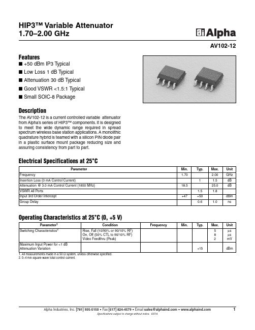
HIP3™ Variable Attenuator 1.70–2.00 GHzFeaturesI +50 dBm IP3 Typical I Low Loss 1 dB Typical I Attenuation 30 dB Typical I Good VSWR <1.5:1 Typical I Small SOIC-8 PackageAV102-12DescriptionThe AV102-12 is a current controlled variable attenuator from Alpha’s series of HIP3™ components.It is designed to meet the wide dynamic range required in spread spectrum wireless base station applications.A monolithic quadrature hybrid is teamed with a silicon PIN diode pair in a plastic surface mount package reducing size and assuring consistency from part to part.Electrical Specifications at 25°CParameter1ConditionFrequencyMin.Typ.Max.Unit Switching Characteristics 2Rise, Fall (10/90% or 90/10% RF)5µs On, Off (50% CTL to 90/10% RF)8µs Video Feedthru (Peak)2mV Maximum Input Power for <1 dB Attenuation Variation+15dBmOperating Characteristics at 25°C (0, +5 V)1.All measurements made in a 50 Ωsystem, unless otherwise specified.2.0–4 mA square wave total control current.V S W R (:1)Input/Output VSWR vs. Current@ 1700 MHz1.01.11.21.31.41.50.00000.00100.00200.00300.00400.0050Current (Amps)InputOutputV S W R (:1)Input/Output VSWR vs. Current@ 1850 MHz1.01.11.21.31.41.5Current (Amps)0.00000.00100.00200.00300.00400.0050InputOutputA t t e n u a t i o n (dB )0.00000.00100.00200.00300.00400.0050Attenuation vs. Current-50.0-40.0-30.0-20.0-10.00.0Current (Amps)A t t e n u a t i o n (dB )1.701.801.902.00Attenuation vs. Frequency-25.0-20.0-15.0-10.0-5.00.0Frequency (GHz)0.0 mA 0.2 mA 0.7 mA1.7 mA2.4 mA3.0 mAInput/Output VSWR vs. Current@ 2000 MHz1.01.11.21.31.41.5Current (Amps)V S W R (:1)0.00000.00100.00200.00300.00400.0050Input OutputD i o d e C u r r e n t (m A )4006008001000Typical PIN Diode Current vs. Voltage0.010.1110Diode Voltage (mV)Typical Performance DataCharacteristicValueRF Input Power .5 W CW, 4 W @ 12.5%Duty Cycle Control Current 50 mA Each Diode Operating Temperature -40 to +85°C Storage Temperature-40 to +85°CMaximum Reverse Diode Voltage -10 V Electrostatic Discharge+125 VAbsolute Maximum RatingsNote:Operating this device above any of these parameters may cause irreversible damage.Recommended Board Layout0.0190 TYP.0.0555 TYP.SOIC-80.0490.016 MAX.0.004 (0.10 mm)0.007 (0.17 mm)8˚PIN 1CONTROL CURRENTGNDRF InGNDGND RF OutCONTROL CURRENT GND Pin OutConnection DiagramMaterial is 10 mil FR4.。
奥的斯中英文对照

:奥的斯中英文对照1 TOP 顶层2 LOBBY 厅外层站基站3 BOTTOM 底层4 CFT—P 餐厅位置5 OPERAT 操作类型6 EN—BSM 允许地下室服务(下集选)7 P1 位置指示器类型8 P1—POS9 P1-OPT10 ELD—fOPG ELD显示前门开门时间11 ELD—fCLG ELD显示前门关门时间12 ELD—rOPG ELD显示后门开门时间13 ELD—rCLG ELD显示后门关门时间14 ELD-LNG ELD显示语种15 ELD-SYm1 ELD显示禁烟信息16 ELD-DOOR ELD门显示类型17 ELD-MSG ELD乘客信息显示18 EN—SFR 允许信号闪烁19 LR-T 轿厢照明20 LR—MODE 风扇照明继电器任选项21 EN-HLC 允许大厅灯在内选操作时亮22 HDL-TYP 大厅方向灯类型23 HL-SET24 CR—DIR 定位运行方向25 CR—DO 后门校正状态26 ERO-TYP 允许ERO限位27 REM——TYP 远程监控模式类型28 CPC-TYP 轿厢位置节点输出类型29 DFCR—DEL30 LW—TYP 称重板类型31 PX2。
132 HWY—TYP33 CPR-T 内选优先时间34 ARD-P 自动返回位置35 ARD-T 自动放回时间36 ARBL—T37 ARBL—PRK 锁梯优先38 PKS-P锁梯位置39 PKS-TYP锁梯类型40 PKS-T锁梯时间。
41 PKS-DO 驻停时门状态42 EN—SHB 允许分开前后厅按钮43 DCP-T 延迟轿厢保护时间44 CTL—DO CTL时门状态45 CTL-P CTL到达位置46 ANS ANS时允许内选数量47 OLD—TYP48 ANS(kg)防捣乱功能49 PEAK(%)50 LNS(%)满载功能51 OLD(%)52 ATT 有司机类型53 ISC 独立服务54 ISPS—TYP55 ISC-T56 SPEECH 语言模式57 CPMT—D58 DCMT-A59 DOMT—O60 DOC 门响应次数(外呼)61 DS-CCB 允许删除轿厢呼叫62 DS—DOB 允许删除DOB/RDOB操作63 EN-RB 内选复位按钮64 DHB-TYP 门保持按钮时间65 PARK-1 驻停位置166 PARK-2 驻停位置267 PARK-3 驻停位置368 PARK—4 驻停位置469 PARK—5 驻停位置570 PARK-6 驻停位置671 PARK-7 驻停位置772 PARK-8 驻停位置873 GRP—NO 电梯在群组中编号74 GROUP 电梯群组中电梯数量75 CNL 轿厢驻停在大厅的数量76 RSR—RSP77 HC-PASS78 MIT-ST 进入高峰触发时间79 MIT—T 进入高峰停止时间80 MIT-VD 不确定派遣间隔81 MIT-DOOR 高峰开门82 MIT-NLB 高峰响应外呼83 DUPK-P 双上高峰位置84 DUPK-G 双上高峰组选择85 MOT—T 退出高峰触发中止时间86 EN-UCB 厅外上呼叫忽略87 TFS—P 分组转换楼层88 EN—ZBS 允许单独地下室驻停89 SEL-COMP 凸轮继电器输出选择90 RNG—BAUD91 L—PARK 大厅驻停操作92 PRKDST93 EN—GSS94 MG—DEL95 DRV—TYP 驱动类型96 EN-ADO 允许提前开门97 SPEED 驱动速度(快速)98 RDR—D99 BRK—TYP 抱闸类型100 DOOR 前门机类型101 REAR 后门机类型102 EN—DDO 允许双门操作103 EN—ADM104 F:DO—TYP 前门开门类型105 F:DC-TYP 前门关门类型106 F:EN—ACG 允许再平层107 F:EN-DCL108 R:DO—TYP 后门开门类型109 R:DC—TYP 后门关门类型110 R:EN—ACG111 R:EN-DCL112 CM-PROT113 LDR 有限门反向114 EN-PMO 允许门时间监测115 EN-NDG 允许强迫关门116 NDG-T 强迫关门启动时间117 EN—CK 允许删除门时间003 118 DW—DLY DW节点延时时间119 TLD—DW—D120 DO—BEL 开门铃时间121 MIN-C 最小轿内门时间122 MAX-C 最大轿内门时间123 MIN—H 最小厅外门时间124 MAX—H 最大厅外门时间125 DOR-T 前门反向时间126 FDOR—T 后门反向时间127 DTC-T 关门保护时间128 DTO—T 开门保护时间129 LOB—NT 大厅门时间130 CFT—NT 餐厅门时间131 SPB-NT 特别开关门按钮时间132 DHB-TYP 门保持按钮操作时间133 WCO—T 盲梯门操作时间134 SHO-T135 SHO—LT136 DAR-T 驱动错误时门时间137 DXT-T 扩展门时间138 DCB-TYP 关门按钮类型139 DZ—TYP 平层感应类型140 EN—RLV 允许反平层141 SPB—TYP SPB板类型142 Encoder 传感器PVT143 SDI-Dir SPB板上七段显示144 BRE-Max 每放一下抱闸电梯所走的距离145 SPB-Temp SPB温度146 ES—TYP 急停类型147 ES—LRCU148 EFO—P EFO操作位置149 EFO—NC150 EFO—DC EFO操作关门时间151 EFO-DO EFO操作开门时间152 EFO-OP153 EFONDG EFO允许NDG154 EFO-REV155 EFO-MP156 EFO-MP-T157 EFO—SD158 EFO—BUZ159 ASL—P 备用消防位置160 EFS-TY EFS类型。
ADAU1513ACPZ资料

Class-D Audio Power StageADAU1513Information furnished by Analog Devices is believed to be accurate and reliable. However Rev. 0, no responsibility is assumed by Analog Devices for its use, nor for any infringements of patents or other rights of third parties that may result from its use. Specifications subject to change without notice. No license is granted by implication or otherwise under any patent or patent rights of Analog Devices. T rademarks and registered trademarks are the property of their respective owners.One Technology Way, P.O. Box 9106, Norwood, MA 02062-9106, U.S.A.Tel: 781.329.4700 Fax: 781.461.3113 ©2007 Analog Devices, Inc. All rights reserved.FEATURESIntegrated stereo power stage R DS-ON < 0.3 Ω (per transistor) Efficiency > 90%Short-circuit protectionOvertemperature protectionAPPLICATIONSFlat panel televisions PC audio systems Mini componentsGENERAL DESCRIPTIONThe ADAU1513 is a 2-channel bridge-tied load (BTL) Class-D audio power stage. The power stage can drive the speaker loads of 4 Ω at up to 15 W per channel at highefficiency. The 4-channel audio system can be formed when used with an ADAV4201 pulse-width modulator (PWM) processor using two ADAU1513s. The power stage accepts a 3.3 V logic differential PWM as input from an ADAV4201 processor. The power stage comprises thermal and output short-circuit protection with logic-level error flag outputs for interfacing to a system microcontroller along with reset and mute control of the power stage. The power stage operates from a range of power supply voltages from 9 V up to 18 V . The low power digital logic operates from a 3.3 V supply. The power stage can be used with modulators other than the ADAV4201. Contact your local sales department for application assistance.FUNCTIONAL BLOCK DIAGRAMINL+INL–INR+INR–AVDDAGNDDVDD06750-001Figure 1.ADAU1513Rev. 0 | Page 2 of 16TABLE OF CONTENTSFeatures..............................................................................................1 Applications.......................................................................................1 General Description.........................................................................1 Functional Block Diagram..............................................................1 Revision History...............................................................................2 Specifications.....................................................................................3 Performance Summary................................................................3 Power Supplies..............................................................................3 Digital I/O.....................................................................................4 PWM Input Logic Table..............................................................4 Digital Timing...............................................................................4 Absolute Maximum Ratings............................................................5 ESD Caution..................................................................................5 Pin Configuration and Function Description..............................6 Typical Performance Characteristics.............................................8 Theory of Operation......................................................................12 Overview.....................................................................................12 Power Stage.................................................................................12 Protection Circuits.....................................................................12 Thermal Protection....................................................................12 Overcurrent Protection.............................................................12 Undervoltage Protection...........................................................12 Automatic Recovery from Protections....................................12 MUTE and STDN ......................................................................13 Power-Up/Power-Down Sequence..........................................13 Applications Information..............................................................15 Outline Dimensions.......................................................................16 Ordering Guide.. (16)REVISION HISTORY5/07—Revision 0: Initial VersionADAU1513Rev. 0 | Page 3 of 16SPECIFICATIONSDVDD = 3.3 V , AVDD = 3.3 V , PVDD = 15 V , ambient temperature = 25°C, load impedance = 8 Ω, measurement bandwidth = 20 Hz to 20 kHz, unless otherwise noted. Audio performance test data measured with ADAV4201.PERFORMANCE SUMMARYTable 1.Parameter Min Typ Max Unit Test Conditions/Comments OUTPUT POWER 1 1 kHz 11 W 1% THD + N, 8 Ω 14 W 10% THD + N, 8 Ω 14.5 W 1% THD + N, 6 Ω 17.5 W 10% THD + N, 6 Ω 19 W 1% THD + N, 4 Ω 23 W 10% THD + N, 4 Ω EFFICIENCY 90 % P OUT = 15 W R DS-ON Per High-Side Transistor 280 mΩ I D = 100 mA Per Low-Side Transistor 250 mΩ I D = 100 mA THERMAL CHARACTERISTICSThermal Warning Active 2135 °C Die temperature Thermal Shutdown Active 150 °C Die temperature OVERCURRENT SHUTDOWN ACTIVE 5 A peak TOTAL HARMONIC DISTORTION PLUS NOISE (THD + N)0.1 % P OUT = 1 W, 1 kHz SIGNAL-TO-NOISE RATIO (SNR) 96 dB A-weighted, referred to 1% THD + N output DYNAMIC RANGE 96 dB A-weighted, measured with −60 dBFS input CROSSTALK BETWEEN LEFT AND RIGHT CHANNELS 65 dB @ 0 dBFS input 20 Hz to 20 kHz UNDERVOLTAGE TRIP THRESHOLD 5 V MINIMUM OUTPUT PULSE WIDTH 50 ns1 Output powers above 15 W at 4 Ω and above 18 W at 6 Ω may need extra heat-sinking for continuous operation. 2Thermal warning flag is for indication of device T J reaching close to shutdown temperature.POWER SUPPLIESADAU1513Rev. 0 | Page 4 of 16DIGITAL I/OTable 3.Parameter Min Typ Max Unit Test Conditions/Comments INPUT VOLTAGE Input Voltage High 2.0 V Input Voltage Low 0.8 V OUTPUT VOLTAGE Output Voltage High 2.4 V @ 2 mA Output Voltage Low 0.4 V @ 2 mA LEAKAGE CURRENT ON DIGITAL INPUTS 10 μAPWM INPUT LOGIC TABLEDIGITAL TIMINGFigure 2. Timing Diagram Unmute06750-031OUTx+/OUTx–STDN MUTEINx+/INx–Figure 3. Timing Diagram MuteADAU1513Rev. 0 | Page 5 of 16ABSOLUTE MAXIMUM RATINGS1Includes any induced voltage due to inductive load.Stresses above those listed under Absolute Maximum Ratings may cause permanent damage to the device. This is a stress rating only; functional operation of the device at these or any other conditions above those indicated in the operationalsection of this specification is not implied. Exposure to absolute maximum rating conditions for extended periods may affect device reliability.ESD CAUTIONADAU1513Rev. 0 | Page 6 of 16PIN CONFIGURATION AND FUNCTION DESCRIPTION06750-003111111122222I N R –I N R +M U T E S T D N T E S T 4T E S T 5D G N D D V D D A V D D A G N D T E S T 6T E S T 7876543210987P G N D P G N D P V D D P V D D P V D D P V D D P V D D P V D D P V D D P V D D P G N D P G N D 123456789101112OUTL–OUTL–OUTL–OUTL+OUTL+OUTL+INL–INL+OTW TEST2TEST3OUTR–OUTR–OUTR+OUTR+OUTR+TEST13TEST12TEST11TEST10TEST9TEST835OUTR–3634333231302928272625ERR NOTES1. EPAD NOT SHOWN AND INTERNALLY CONNECTED TO PGND, DGND, AND AGND FOR TQFP-48.2. EPAD NOT SHOWN AND INTERNALLY CONNECTED TO PGND AND DGND FOR LFCSP-48.Figure 4. Pin ConfigurationADAU1513Pin Number Mnemonic Type1Description34, 35, 36 OUTR− O Output of High Power Transistors, Right Channel Negative Polarity.37, 38, 47, 48 PGND P Power Ground for High Power Transistors. Internally connected to ePAD2.39, 40, 41, 42, 43, 44, 45, 46 PVDD P Positive Power Supply for High Power Transistors.1 I = input, O = output, P = power.2ePAD is connected internally to PGND, DGND, and AGND.Rev. 0 | Page 7 of 16ADAU1513Rev. 0 | Page 8 of 16TYPICAL PERFORMANCE CHARACTERISTICS06750-004OUTPUT POWER (W)T H D + N (d B )–80–20–70–60–50–40–3010m 10100m 1Figure 5. THD + N vs. Output Power, 9 V, 4 Ω06750-005OUTPUT POWER (W)T H D + N (d B )–80–20–70–60–50–40–3010m 10100m 1Figure 6. THD + N vs. Output Power, 9 V, 6 Ω06750-006OUTPUT POWER (W)T H D + N (d B )–80–20–70–60–50–40–3010m10100m 1Figure 7. THD + N vs. Output Power, 9 V, 8 Ω 06750-007OUTPUT POWER (W)T H D + N (d B )–80–20–70–60–50–40–3010m10100m1Figure 8. THD + N vs. Output Power, 12 V, 4 Ω06750-008OUTPUT POWER (W)T H D + N (d B )–80–20–70–60–50–40–3010m10100m 1Figure 9. THD + N vs. Output Power, 12 V, 6 Ω06750-009OUTPUT POWER (W)T H D + N (d B )–80–20–70–60–50–40–3010m10100m 1Figure 10. THD + N vs. Output Power, 12 V, 8 ΩADAU1513Rev. 0 | Page 9 of 1606750-010OUTPUT POWER (W)T H D + N (d B )–80–20–60–50–4010m10100m1–30–70Figure 11. THD + N vs. Output Power, 15 V, 4 Ω06750-011OUTPUT POWER (W)T H D + N (d B )–80–20–70–60–50–40–3010m10100m 1Figure 12. THD + N vs. Output Power, 15 V, 6 Ω06750-012OUTPUT POWER (W)T H D + N (d B )–80–20–70–60–50–40–3010m10100m 1Figure 13. THD + N vs. Output Power, 15 V, 8 Ω 06750-013FREQUENCY (kHz)O U T P U T (d B r )–160–150–140–130–120–110–100–90–80–70–60–50–40–30–20–10002204681012141618Figure 14. FFT, 1 W, 15 V, 8 Ω06750-014FREQUENCY (kHz)O U T P U T (d B r )–160–150–140–130–120–110–100–90–80–70–60–50–40–30–20–100Figure 15. FFT, 60 dBFS, 15 V, 8 Ω06750-015FREQUENCY (kHz)O U T P U T (d B V )–140–120–110–100–90–80–70–60–50–40–30–10–2002010–130Figure 16. FFT Dither, 15 V, 8 ΩADAU1513Rev. 0 | Page 10 of 1606750-016FREQUENCY (Hz)T H D + N (d B )–800–75–70–65–60–55–50–45–40–35–30–25–20–15–10–5201001k10kFigure 17. THD + N vs. Frequency, 1 W, 15 V, 8 Ω06750-017FREQUENCY (Hz)C R O S S T A L K (d B )–100–90–80–70–60–50–40–30–20–10Figure 18. Crosstalk, 0 dBFS, 15 V, 8 Ω06750-018T AMBIENT (°C)P D I S S M A X (W )01234560102030405060708090100110120130140150160Figure 19. Power Dissipation vs. Ambient Temperature 06750-019OUTPUT POWER (W)E F F I C IE N C Y (%)0510********102030405060708090Figure 20. Efficiency vs .Output Power, 15 V, 4 Ω06750-020OUTPUT POWER (W)E F F I C I E N C Y (%)5101520250102030405060708010090Figure 21. Efficiency vs. Output Power, 15 V, 6 Ω06750-021OUTPUT POWER (W)E F F I C I EN C Y (%)0510152025102030405060708010090Figure 22. Efficiency vs. Output Power, 15 V, 8 ΩADAU151306750-022PVDD (V)O U T P U T P O W E R (W )0302551015206188971012111413161715Figure 23. Output Power vs. PVDD, 40 dB THD + N06750-023PVDD (V)O U T P U T P O W E R (W )4025510152061889710121114131617153530Figure 24. Output Power vs. PVDD, 20 dB THD + N06750-024OUTPUT POWER PER CHANNEL, STEREO MODE (W)P O W E R D I S S I P A T I O N (W )12345678910111213141505101520253035Figure 25. Power Dissipation vs. Output Power, 4 Ω06750-025OUTPUT POWER PER CHANNEL, STEREO MODE (W)P O W E R D I S S I P A T I O N (W )1234560510152025Figure 26. Power Dissipation vs. Output Power, 6 Ω06750-026OUTPUT POWER PER CHANNEL, STEREO MODE (W)P O W E R D I S S I P A T I O N (W )12305101520Figure 27. Power Dissipation vs. Output Power, 8 ΩADAU1513 THEORY OF OPERATIONOVERVIEWThe ADAU1513 is a 2-channel integrated power stage designed to accept the logic level PWM inputs. The PWM inputs are amplified, low-pass filtered using a simple passive LC network, and then can be used to drive the speaker loads. The power stage has built-in circuits for overtemperature, overcurrent, short-circuit, and undervoltage protection.POWER STAGEThe 2-channel ADAU1513 power stage comprises a total of eight half bridges. Each half bridge is made up of PMOS and NMOS devices. The gate drive for the respective FETs is generated internally and does not need a special gate drive supply or bootstrap capacitor compared to all NMOS stages. This simplifies the high-side driver design and requires less external components.PROTECTION CIRCUITSThe ADAU1513 includes comprehensive protection circuits.It includes thermal warning, thermal overheat, and overcurrent or short-circuit protection on the outputs. The ERR and OTW outputs are open drain, requiring external pull-up resistors. The outputs are capable of sinking 10 mA. The open-drain outputs are useful in multichannel applications where more than one ADAU1513 are used. The error outputs of multiple ADAU1513s can be OR’e d to simplify the system design. The logic outputs of the error flags ease the system design using a microcontroller.The power stage does not consist of protection in case PWM input stays high continuously. In such a case, the output pro-duces dc and it is possible to damage the speaker. To prevent this, ensure that the modulator is switching whenever the power stage is turned on.THERMAL PROTECTIONThermal protection in the ADAU1513 is categorized into two error flags: one as thermal warning and the other as thermal shutdown. When the device junction temperature reaches near 135°C (±5°C) the ADAU1513 outputs a thermal warning error flag by pulling OTW (Pin 10) low. This flag can be used by the microcontroller in the system as an indication to the user or can be used to lower the input level to the amplifier to prevent the thermal shutdown. The device continues operation until shutdown temperature is reached.When the device junction temperature exceeds 150°C the device outputs an error flag by pulling the ERR (Pin 9) low. This error flag is latched. To restore the operation, MUTE (Pin 16) needs to be toggled to low and then to high again. OVERCURRENT PROTECTIONThe overcurrent protection in the ADAU1513 is set internally at 5 A peak output current. The device protects the output devices against excessive output current by pulling the (Pin 9) low. This error flag is latched type. To restore the normal operation, MUTE (Pin 16) needs to be toggled to low and then to high again. The error flag is useful for the microcontroller in the system to indicate an abnormal operation and to initiate the audio MUTE sequence. The device senses the short-circuit condition on the outputs after the LC filter. Typical short-circuit conditions include shorting of the output load and shorting to either PVDD or GND.UNDERVOLTAGE PROTECTIONThe ADAU1513 has an undervoltage protection circuit that senses the undervoltage on PVDD. When the PVDD supply goes below the operating threshold, the output FETs are turned to a high-Z condition. Also, the device issues an error flag by pulling the ERR pin low. This condition is latched. To restore the operation, MUTE (Pin 16) needs to be toggled to low and then to high again.AUTOMATIC RECOVERY FROM PROTECTIONSIn certain applications, it is desired for the amplifier to recover itself from thermal protection without the need for system microcontroller intervention.The ADAU1513 thermal protection circuit issues two error signals for this purpose: one thermal warning (OTW) and the other thermal shutdown (ERR).With these two error signals, there are two options for using the protections:•Option 1: Using OTW•Option 2: Using ERRThe following sections provide further details of these two options.Option 1: Using OTWThe OTW pin is pulled low when the die temperature reaches 130°C to 135°C This pin can be wired to the pin using an RC circuit as shown in Figure 28.675-27TO MUTELOGIC INPUTFigure 28. Option 1 Schematic for AutorecoveryThe low logic level on OTW also pulls down the MUTE pin. The bridge is shut down and, therefore, starts cooling or the die temperature starts reducing. When it reaches 120°C, the OTW signal starts going high. While this pin is tied to a capacitor with a resistor pulled to DVDD, the voltage on this pin starts rising slowly towards DVDD. When it reaches the input logic high threshold, MUTE is deasserted and theADAU1513amplifier starts functioning again. This cycle repeats itself depending on the input signal conditions and the temperature of the die. This option allows part operation that is safely below the shutdown temperature of 150°C and allows the amplifier to recover itself without the need for microcontroller intervention.Option 2: Using ERROption 2 is similar to Option 1 if the ERR pin can be tied to MUTE instead of OTW . See the circuit in Figure 29.06750-028TO MUTE LOGIC INPUTFigure 29. Option 2 Schematic for AutorecoveryIn this case, the part goes into shutdown mode due to any of the error-generating events like output overcurrent, overtemperature, missing PVDD or DVDD, or clock loss. The part recovers itself based on the same circuit operation in Figure 28.However, if the part goes into error mode due to overtempera-ture, then the device would have reached its maximum limit of 150°C (15°C to 20°C higher than Option 1). If it goes into error mode due to an overcurrent from a short circuit on the speaker outputs, then the part will keep itself recycling on and off until the short circuit is removed.It is possible that, with this operation, the part is subjected to a much higher temperature and current stress continuously. This, in turn, reduces the part’s reliability in the long term. Therefore, using Option 1 for autorecovery from the thermal protection and using the system microcontroller to indicate to the user of an error condition is recommended.MUTE AND STDNThe MUTE and STDN are 3.3 V logic-compatible inputs used to control the turn-on/turn-off for ADAU1513.The STDN input is active low when the STDN pin is pulled low and the device is in its energy-saving mode. The power stage is in high-Z state. The high logic level input on the STDN pin will wake up the device. The logic circuits are running internally but the power stage is still in high-Z state.When the MUTE pin is pulled high, the power stage is active and starts responding to PWM inputs. The low level on the MUTE pin disables the power stage and is recommended to be used to mute the audio output. See the Power-Up/Power-Down Sequence section for more details.POWER-UP/POWER-DOWN SEQUENCEFigure 30 shows the recommended power-up sequence for the ADAU1513.06750-029AVDD/DVDDPVDDFigure 30. Recommended Power-Up SequenceThe ADAU1513 does not have any pop-and-click suppression circuits; therefore, care must be taken during the power-up. The power stage stays in Hi-Z on power-up. However, it is recom-mended to ensure that STDN and MUTE are held low during initial power-up. First, STDN should be pulled high followed by MUTE to turn on the power stage. The power stage turns on after the MUTE signal is pulled high and responds to PWM inputs after a small propagation delay of 200 μs.The special turn-on sequence may be necessary depending on the PWM used to prevent the turn-on pop or click. However, if the ADAV4201 processor is used, the processor has a built-in special turn-on PWM sequence. The processor sends a unique PWM input start sequence that ensures soft turn-on.If another modulator is used, care must be taken to ensure that the modulator has built-in pop-and-click suppression. Also, because the power stage does not track the PWM inputs, it is recommended to use the system microcontroller to ensure that the modulator is ready to send the PWM sequence before turning on the power stage.Similarly, for muting the amplifier, it may be necessary tosupply a special muting PWM sequence for minimum pop and click. The ADAV4201 processor has a built-in feature that takes care of this need. If any other modulator is used, care must be taken during muting of the power stage.The system microcontroller can be used to handle the mute/unmute of the power stage as well as a modulator. The error outputs of the power stage should be connected to the microcontroller port. This error flag can be used to inform the modulator that the power stage is shut down and to mute the PWM inputs. On removal of the error condition, the microcontroller should initiate an unmute sequence to mini-mize pop and click while power stage is turning on/turning off. The ADAU1513 uses three separate supplies: AVDD (3.3 V analog for internal reference), DVDD (3.3 V digital for control logic and clock oscillator), and PVDD (9 V to 18 V power stage and level shifter). Separate pins are provided for the AVDD,ADAU1513DVDD, and PVDD supply connections, as well AGND, DGND, and PGND.In addition, the ADAU1513 incorporates a built-in undervoltage lockout logic on DVDD as well as PVDD. This helps detect undervoltage operation and eliminates the need to have an external mechanism to sense the supplies.The ADAU1513 monitors the DVDD and PVDD supply voltages and prevents the power stage from turning on if either of the supplies are not present or below the operating threshold. Therefore, if DVDD is missing or below the operating thresh-old, for example, the power stage will not turn on, even if the PVDD is present or vice versa.Because this protection is only present on DVDD and PVDD and not on AVDD, shorting both AVDD and DVDD externally or generating AVDD and DVDD from one power source is recommended. This ensures both AVDD and DVDD supplies are tracking each other and avoids the need to monitor the sequence with respect to PVDD. This also ensures minimal pop and click during power-up. When using separate AVDD and DVDD supplies, ensure that both supplies are stable before unmuting or turning on the power stage.During power-up, it is recommended to keep STDN and MUTE low to ensure that the power stage stays in high-Z mode. Similarly, during shutdown, pulling MUTE to logic low before pulling STDN down is recommended. However, where a fault event occurs, the power stage will shut down to protect the part. In this case, depending on the signal level, there is some pop at the speaker.During shutdown of the power supplies to reduce power consumption, it is highly recommended to mute the amplifier first, followed by pulling STDN low before shutting down any of the supplies. After MUTE is pulled low, the power supplies can be shut down in the following order: PVDD, DVDD, then AVDD. Where AVDD and DVDD are generated from a single source, ensure that PVDD is tuned off before DVDD and AVDD, and after issuing MUTE and STDN.ADAU1513APPLICATIONS INFORMATIONRefer to the application schematic in Figure 31 for details on connections and component values. For details on the PWM modulator part, refer to the ADAV4201 data sheet.For applications with PVDD > 15 V , add components R1 and R2 = 10 Ω typical, C5 and C6 = 680 pF typical, and D1 through D8 = CRS01/02.06750-030Figure 31. Application SchematicTable 8. Suggested Low-Pass Filter ValuesLoad Impedance (Ω) Inductance L1 to L4 (μH)Capacitance C1 to C4 (μF)4 10 1.56 15 1 8 220.68ADAU1513OUTLINE DIMENSIONS1.000.850.80PLANECOMPLIANT TO JEDEC STANDARDS MO-220-VKKD-2Figure 32. 48-Lead Lead Frame Chip Scale Package [LFCSP_VQ]7 mm × 7 mm Body, Very Thin Quad(CP-48-1)Dimensions shown in millimetersCOMPLIANT TO JEDEC STANDARDS MS-026-ABCLEAD PITCH0.270.220.17ROTATED 90° CCW042507-AFigure 33. 48-Lead Thin Quad Flat Package, Exposed Pad [TQFP_EP](SV-48-5)Dimensions shown in millimetersORDERING GUIDEModelTemperatureRange PackageDescription PackageOption ADAU1513ACPZ 1−40°C to +85°C 48-Lead Lead Frame Chip Scale Package [LFCSP_VQ] CP-48-1 ADAU1513ACPZ-RL 1−40°C to +85°C 48-Lead Lead Frame Chip Scale Package [LFCSP_VQ], 13” Tape and Reel CP-48-1 ADAU1513ACPZ-RL71−40°C to +85°C 48-Lead Lead Frame Chip Scale Package [LFCSP_VQ], 7” Tape and Reel CP-48-1 ADAU1513ASVZ 1−40°C to +85°C 48-Lead Thin Quad Flat Package, Exposed Pad [TQFP _EP] SV-48-5 ADAU1513ASVZ-RL 1−40°C to +85°C 48-Lead Thin Quad Flat Package, Exposed Pad [TQFP _EP], 13” Tape and Reel SV-48-5 ADAU1513ASVZ-RL71−40°C to +85°C 48-Lead Thin Quad Flat Package, Exposed Pad [TQFP _EP], 7” Tape and Reel SV-48-51Z = RoHS Compliant Part.©2007 Analog Devices, Inc. All rights reserved. Trademarks and registered trademarks are the property of their respective owners. D06750-0-5/07(0)。
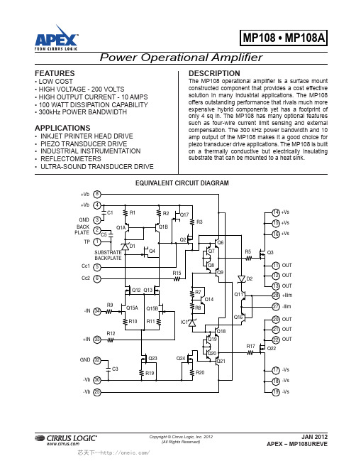
MP108FD,MP108FDA, 规格书,Datasheet 资料
(Note 4) Full temp range
TEMPERATURE RANGE, case
MP108 Min Typ Max
+VS - 10 +VS - 8.6 -VS + 10 -VS + 7
+VS - 1.6
-VS +
1
5
300
±15
±75 ±100
50
65
1
1.25
1. Unless otherwise noted: TC = 25°C, CC = 100pF. DC input specifications are value given. Power supply voltage is typical rating.
2. Long term operation at the maximum junction temperature will result in reduced product life. Derate internal power dissipation to achieve high MTTF.
OFFSET VOLTAGE, vs. temperature
Full temp range
OFFSET VOLTAGE, vs. supply
BIAS CURRENT, initial (Note 3)
BIAS CURRENT, vs. supply
OFFSET CURRENT, initial
INPUT RESISTANCE, DC
POWER DISSIPATION, internal, DC
INPUT VOLTAGE
TEMPERATURE, pin solder, 10s
STTH6003CW;中文规格书,Datasheet资料
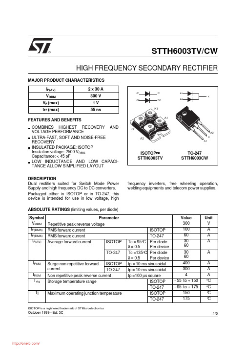
STTH6003TV/CWOctober 1999 - Ed: 5CHIGH FREQUENCY SECONDARY RECTIFIER®Dual rectifiers suited for Switch Mode Power Supply and high frequency DC to DC converters.Packaged either in ISOTOP or in TO-247, this device is intended for use in low voltage, high frequency inverters, free wheeling operation,welding equipments and telecom power supplies.DESCRIPTIONCOMBINES HIGHEST RECOVERY AND VOLTAGE PERFORMANCEULTRA-FAST, SOFT AND NOISE-FREE RECOVERYINSULATED PACKAGE: ISOTOP Insulation voltage: 2500 V RMS Capacitance: < 45 pFLOW INDUCTANCE AND LOW CAPACI-TANCE ALLOW SIMPLIFIED LAYOUT FEATURES AND BENEFITSSymbol ParameterValue Unit V RRM Repetitive peak reverse voltage 300V I F(RMS)RMS forward current ISOTOP 100A I F(RMS)RMS forward current TO-24760A I F(AV)Average forward current ISOTOPTc = 95°C δ = 0.5Per diode Per device 3060A TO-247Tc =135°C δ = 0.5Per diode Per device 3060A I FSM Surge non repetitive forward current.ISOTOP tp = 10 ms sinusoidal 400A TO-247tp = 10 ms sinusoidal 300A I RSMNon repetitive peak reverse current tp =100 µs square4A T stg Storage temperature rangeISOTOP - 55 to + 150°C TO-247- 65 to + 175°C TjMaximum operating junction temperatureISOTOP 150°C TO-247175°CABSOLUTE RATINGS (limiting values, per diode)I F(AV) 2 x 30 A V RRM 300 V V F (max) 1 V trr (max)55 nsMAJOR PRODUCT CHARACTERISTICSA1K1K2A2A1A2K1K2ISOTOP ™STTH6003TV ISOTOP is a registered trademark of STMicroelectronicsA1K A2A1A2KTO-247STTH6003CW1/6Symbol Parameter Tests conditionsMin.Typ.Max.Unit I R *Reverse leakage currentV R = 300 VTj = 25°C 60µATj = 125°C60600V F **Forward voltage dropI F = 30 ATj = 25°C 1.25V Tj = 125°C0.851Pulse test : * tp = 5 ms, δ < 2 % ** tp = 380 µs, δ < 2%To evaluate the maximum conduction losses use the following equation:P = 0.75 x I F(AV) + 0.008 x I F 2(RMS)STATIC ELECTRICAL CHARACTERISTICS (per diode)Symbol ParameterValue Unit R th (j-c)Junction to caseISOTOP Per diodeTotal 1.40.75°C/WTO-247Per diode Total 10.55R th (c)Coupling0.1When the diodes 1 and 2 are used simultaneously:∆Tj (diode 1) = P (diode 1) x R th(j-c) (per diode) + P (diode 2) x R th(C)THERMAL RESISTANCES Symbol Tests conditionsMin.Typ.Max.Unit trrI F = 0.5 A Irr = 0.25 A I R = 1A Tj = 25°C40nsI F= 1 A dI F /dt = - 50 A/µs V R = 30 V 55tfr I F = 30 A dI F /dt = 200 A/µs Tj = 25°C 350ns V FP V FR = 1.1 x V F max.5V S factor Vcc = 200 V I F = 30 A Tj = 125°C0.3-I RMdI F /dt = 200 A/µs11A RECOVERY CHARACTERISTICS STTH6003TV/CW2/65101520253035400510152025303540IF(av) (A)P1(W)Tδ=tp/Ttpδ= 1δ= 0.5δ= 0.2δ= 0.1δ= 0.05Fig. 1: Conduction losses versus average current (per diode).0.20.40.60.81.01.21.41.61.82.02.22.42.6110100VFM(V)IFM(A)Tj=125°C T ypical valuesTj=25°C Maximum valuesTj=125°C Maximum valuesFig. 2: Forward voltage drop versus forward current (maximum values , per diode).05010015020025030035040045050020406080100120140160180trr(ns)VR=200V Tj=125°CIF=2*IF(av)IF=IF(av)IF=0.5*IF(av)dIF/dt(A/µs)Fig. 5: Reverse recovery time versus dI F /dt (90%confidence, per diode).50100150200250300350400450500246810121416182022dIF/dt(A/µs)IRM(A)VR=200V Tj=125°CIF=2*IF(av)IF=IF(av)IF=0.5*IF(av)Fig. 4: Peak reverse recovery current versus dI F /dt (90% confidence, per diode).1E-31E-21E-11E+01E+10.00.20.40.60.81.0tp(s)Zth(j-c)/Rth(j-c)Tδ=tp/TtpSingle pulse δ= 0.5δ= 0.2δ= 0.1Fig. 3a: Relative variation of thermal impedance junction to case versus pulse duration (ISOTOP).1E-41E-31E-21E-11E+00.00.20.40.60.81.0Zth(j-c)/Rth(j-c)Tδ=tp/Ttptp(s)Single pulseδ= 0.5δ= 0.2δ= 0.1Fig. 3b: Relative variation of thermal impedance junction to case versus pulse duration (TO-247).STTH6003TV/CW3/62550751001250.00.20.40.60.81.01.21.41.61.82.02.22.4Tj(°C)IRMS factorFig. 7: Relative variation of dynamic parameters versus junction temperature (reference: Tj = 125°C).50100150200250300350400450500246810VFP(V)IF=IF(av)Tj=125°CdIF/dt(A/µs)Fig. 8: Transient peak forward voltage versus dI F /dt (90% confidence, per diode).050100150200250300350400450500100200300400500tfr(ns)IF=IF(av)VFR=1.1*VFmaxTj=125°CdIF/dt(A/µs)Fig. 9: Forward recovery time versus dI F /dt (90%confidence, per diode).0501001502002503003504004505000.00.10.20.30.40.50.6S factor VR=200V Tj=125°CdIF/dt(A/µs)Fig. 6: Softness factor (tb/ta) versus dI F /dt (typical values, per diode).STTH6003TV/CW4/6PACKAGE MECHANICAL DATA ISOTOPREF.DIMENSIONS Millimeters Inches Min.Max.Min.Max.A11.8012.200.4650.480 A18.909.100.3500.358 B7.88.200.3070.323 C0.750.850.0300.033 C2 1.95 2.050.0770.081 D37.8038.20 1.488 1.504 D131.5031.70 1.240 1.248 E25.1525.500.990 1.004 E123.8524.150.9390.951 E224.80 typ.0.976 typ.G14.9015.100.5870.594 G112.6012.800.4960.504 G2 3.50 4.300.1380.169 F 4.10 4.300.1610.169 F1 4.60 5.000.1810.197 P 4.00 4.300.1570.69P1 4.00 4.400.1570.173 S30.1030.30 1.185 1.193STTH6003TV/CW5/6Information furnished is believed to be accurate and reliable. However, STMicroelectronics assumes no responsibility for the consequences of use of such information nor for any infringement of patents or other rights of third parties which may result from its use. No license is granted by implication or otherwise under any patent or patent rights of STMicroelectronics. Specifications mentioned in this publication are subject to change without notice. This publication supersedes and replaces all information previously supplied.STMicroelectronics products are not authorized for use as critical components in life support devices or systems without express written ap-proval of STMicroelectronics.The ST logo is a registered trademark of STMicroelectronics © 1999 STMicroelectronics - Printed in Italy - All rights reserved.STMicroelectronics GROUP OF COMPANIESAustralia - Brazil - China - Finland - France - Germany - Hong Kong - India - Italy - Japan - MalaysiaMalta - Morocco - Singapore - Spain - Sweden - Switzerland - United Kingdom - U.S.A.PACKAGE MECHANICAL DATA TO-247F2F1V2L4L2L1L3DLL5MEHVVADia.F3F4G = =F(x3)REF.DIMENSIONSMillimeters Inches Min.Typ.Max.Min.Typ.Max.A 4.85 5.150.1910.203D 2.20 2.600.0860.102E 0.400.800.0150.031F 1.00 1.400.0390.055F1 3.000.118F2 2.000.078F3 2.00 2.400.0780.094F4 3.00 3.400.1180.133G 10.900.429H 15.4515.750.6080.620L 19.8520.150.7810.793L1 3.70 4.300.1450.169L218.500.728L314.2014.800.5590.582L434.60 1.362L5 5.500.216M 2.00 3.000.0780.118V 5°5°V260°60°Dia. 3.55 3.650.1390.143Ordering code Marking Package Weight Base qty Delivery modeSTTH6006TV1STTH6006TV ISOTOP 27gwithout screws10with screwsTubeSTTH6006CW STTH6006CW TO-247 4.36g30TubeCooling method: by conduction (C)Recommended torque value (ISOTOP): 1.3 N.m.Recommended torque value (TO-247°: 0.8 N.m.Maximum torque value (ISOTOP): 1.5 N.m.Maximum torque value (TO-247): 1.0 N.m.Epoxy meets UL 94,V0STTH6003TV/CW6/6分销商库存信息: STMSTTH6003CW。
民航eterm指令大全

机票预订的知识指令城市代码机场代码应聘国际机票出票员,我猜你应该是没做过这个行业的,其实机票出票员的工作很简单,不过要是没练习过或是没有人指导过的话入门可能有点难。
所以我建议你,如果有认识这行的朋友的话,最好是到售票处先实习下,或是你从网站上找个eterm系统操作手册(航空售票系统)民航eterm指令大全登录1.进入系统>$$open tipc32.输入工作号>si:工作号/密码3.查看pid状态>da4.退出系统>so5.修改密码>an:旧密码/新密码6.随时查看sign-in信息>siif:7.指令使用帮助>help: 指令8.屏幕向上一页>pb9.屏幕向下一页>pn10.清屏指令>cp11.重复显示当前页>pg12.一屏显示所有内容>pq1--------------------------------------------------------------------------------查询1. 航班座位可利用显示>av: h/城市对/日期/时间/ 航空公司代码(或gds代码)2. 最早有座位航班查询>fv: 城市对/日期/起飞时间/座位数/航空公司代码(或gds代码)/经停标志/ 舱位3. 航班飞行周期的查询>sk: 城市对/日期/时间/航空公司代码/ 舱位4. 航班经停点和起降时间的显示指令>ff: 航班号/日期5. 指定日期的航段上的航班详细信息显示>dsg:c/航班号/座位等级/日期/航段或rt之后,>dsg: 航班序号--------------------------------------------------------------------------------信息查询及辅助功能一、24小时北京天气预报wf >wf 城市三字代码二、机场转机信息查询dsm >dsm: pek三、机场、国家、航空公司代码查询cntd/cd1)查询城市三字代码>cntd t/beijing2)查询城市名称>cd pek3)查询一个国家所有城市>cntd a/cn4)查询国家全称>cntd c/cn5)查询国家两字码>cntd n/china6)查询航空公司信息>cntd d/ca7)查询航空公司两字代码>cntd m/air china四、计算co1)四则运算>co 100+22)计算北京和巴黎的时差>co t/pekcdg3)显示巴黎10月1日0点的gmt标准时间>co t/cdg/1oct/00004)英里换算成公里>co k/英里数5)公里换算成英里>co m/公里数五、日期查询date1)显示当前日期和星期几>date2)显示10天,90天后的日期>date 10/903)显示2004年1月1日的前2天,及后20天的日期>date 1jan04/-2/20六、时间查询time1)显示当前时间>time2)北京时间2004年1月1日零点的巴黎时间>time 1jan04/0000/cdg3)纽约时间2004年1月1日零点的北京、巴黎时间>time nyc/1jan/0000/pek/cdg七、长度、重量、温度换算cv1)100公里换算成英里>cv 100km2)100英里换算成公里>cv 100mi3)摄氏35度转化为华氏度>cv 35c4)华氏95度转化为摄氏度>cv 95f5)10英镑转化为公斤>cv 10lb6)10公斤转化为英镑-磅>cv 10kg八、查询中文信息yi1)显示所有静态信息的目录>yi2)显示不含副标题的公告>yi标题3)显示有副标题的公告>yi i/某标题九、旅游信息查询tim1)查询签证信息>tim tifv2)查询健康检疫信息>tim tifh3)同时查询签证、健康检疫信息>tim tifa4)查询与出入境有关的信息>tim tidft/城市/章节/小标题/页码5)显示tim帮助功能>tim tihelp6)显示tim中有关规则>tim tirules7)显示综合旅游信息新闻>tim tinews8)显示下一页>tipn9)显示上一页>tipb--------------------------------------------------------------------------------建立pnr一、航段预订1)直接建立航段组ss>ss ca1537/y/1oct/peknkgnn1/1225 14002)间接建立航段组sd>av pekcan>sd 1y13)open航段的建立sn>sn yy/f/pekcan>sn cz/f/pekcan4)arnk段的建立sa >sa tsnpek5) 旅客行程提示>sa mu5119y1oct shapek hk6)调整航段顺序cs>cs 2/1二、姓名输入nm1)英文姓名的输入>nm 1stephen/haetti 1zhu/qi2)同姓旅客英文名的输入>nm 2zhang/jian/qiang3)中文姓名的输入>nm 1杨振振1马永4)无人陪伴儿童姓名输入>nm 1马晓涌(um4)5)带一个婴儿的成人输入姓名>nm 1马永>xn in/马晓涌inf(mar01)p16)建立一个团名为changyou的12人的团体pnr>gn 12changyou三、联系方式ct >ct pek/1234567四、证件信息输入ssr (注意:ca表示相应的航空公司代码)1) 国内旅客>ssr foid ca hk/证件代码及号码/pn 证件种类代码:ni-身份证;pp-护照;id-其他证件2) 国际旅客>ssr pspt ca hk/护照号码/国籍/旅客生日/旅客姓/旅客名/性别及婴儿标识/持有人标识/pn注:下划线部分为必输项五、出票时限tktl>tk tl/1200/01oct/bjs123七、票价信息的简易输入fc/fn 八、选择制定航段进行票价计算或打票sel>sel: 指定航段序号九、国内bsp客票自动生成fn/fc/fp项:>pat:十、国际客票经过qte/xs fsq, 自动生成fn/fc项:>dfsq:十一、付款方式组fp>fp:cash/ check,cny十二、签注信息组ei 十三、旅游代码组tc (一般按照航空公司要求输入) 十四、打票预览tktv>tktv: 打票机序号十五、票号自动传输stn>stn: 票号/pn/指定航段序号十六、客票打印dz打印pnr中所有人的客票>dz:1仅打印第一个成人所携带的婴儿客票>dz:1/p1, inf仅打印第一个成人的客票>dz:1/p1, adl打印pnr中所有婴儿客票>dz:1,inf打印pnr中所有成人客票>dz:1, adl--------------------------------------------------------------------------------特殊服务ssr一、查看航班座位图adm>adm:航段序号/航段二、进行机上座位预订asr>asr: 航段序号/座位号三、里程输入>ssr fqtv承运航空公司代码hk1/发卡航空公司代码卡号/pn四、其他特殊服务的申请>ssr 特殊服务代码航空公司nn数量/pn/sn常用特殊服务代码:机位申请nssa:无烟靠走廊的座位nssw:无烟靠窗的座位nsst:无烟座位smsa:吸烟靠走廊的座位smsw:吸烟靠窗的座位smst:吸烟座位特殊餐食avml:亚洲素食blml:流食chml:儿童餐dbml:糖尿病患者餐fpml:水果拼盘sfml:海洋餐hfml:高纤维餐hnml:印度餐bbml:婴儿餐ksml:犹太教餐lcml:低卡路里餐lfml:低胆固醇、低脂肪餐lsml:无盐餐moml:穆斯林餐vlml:素食(含糖、鸡蛋) vgml:素食(无糖)其他petc:宠物(需要详细说明) bsct:摇篮车/吊床/婴儿摇篮bike:自行车(须说明数量) slpr:机舱内床铺(不包括担架)blnd:盲人旅客(如果有导盲犬或其他动物陪伴,须详细说明)bulk:超大行李(须说明数量、重量和尺寸)cbbg:放置机舱行李(购买了额外座位,须说明数量,重量及尺寸)deaf:聋哑旅客(如果有助听狗或其他动物陪伴,须详细说明)depa:被驱逐出境(有人陪伴) depu:被驱逐处境(无人陪伴)xbag:额外行李(须说明数量、重量和尺寸)frag:易碎行李(须说明数量、重量和尺寸)meda:健康状况(需要旅客医疗状况证明)speq:体育设施(须指明设备类型、数量、重量和尺寸)stcr:担架旅客umnr:无人陪伴儿童--------------------------------------------------------------------------------pnr提取和修改一、pnr提取1)记录编号提取pnr >rt 记录编号2)根据旅客名单提取pnr >rt旅客姓名/航班号/日期3)提取完整pnr >rt c/记录编号4)提取pnr的历史部分>rt u5)返回到pnr的现行部分>rt a6)按照航班的旅客名单提取>ml c/ca1301/10dec >rt 序号7) 提取本部门在该航班的所有订座记录(rr、hk、hn、hl、hx)>ml c/ca1321/7oct8)提取所有团体pnr记录>ml g/ca1321/7oct9)提取所有订妥座位的记录>ml b/ca1321/7oct10)提取所有未证实座位的记录>ml u/ca1321/7oct11)提取所有非团体pnr记录>ml ng/ca1321/7oct二、国内航空公司记录的提取和转换>rrt: v/航空公司记录编号/航班号/日期>@ok三、记录分离sp >sp 1/3四、记录修改1)旅客姓名修改>1/1杨振2)删除姓名组以外的内容>xe 序号3)取消pnr>xepnr@五、记录封口@1)正常封口>@2)以下几种情况可使用@k封口>@ka)将kk,kl或tk变为hkb)将uu,us或tl变为hlc)将tn变为hnd)将带有ni,uc,un的项移到pnr的历史部分3)以下情况可使用@i封口>@ia)航段不连续b)有航班变更标识c)两个连接航段的停留时间小于最小连接时间--------------------------------------------------------------------------------公布运价的查询一、国内公布运价查询:1).查询城市对间当前可用票价fd>fd:城市对/日期/航空公司代码/查询选项(s排序由低到高;l最低价)2).运价限制条件信息查询pfn>pfn: 规则号/ 承运人或在fd的基础上>pfn: 运价序号3).查询运价的航线限制pfr在fd基础上有航线限制标识的情况下>pfr: 运价序号二、航空公司净价查询:(需要航空公司授权)1.查询运价总则>nfn:gr00/ca2.按城市对查询票价信息:>nfd:peklon/ca3.指定旅行日期查询:>nfd:peklon/21may04/ca4.查询单程票价>nfd:peklon/ca*ow5.查询m舱票价>nfd:peklon/ca#m6.查询运价基础为hit的票价>nfd:peklon/ca@hit7.查询学生票价>nfd:peklon/ca*sd8.查询团队票价>nfd:peklon/ca*gc9.显示第3条票价的规则限制>nfn:310.显示第3条票价的航线规定>nfr:311.显示第4条票价的签注信息>nfe:412. 修改查询条件,快速重新查询票价:>nfc:13.指定航线查询>nfq:pek15may04lonpek/ca14. 按协议查询>nfl:/ca15. 显示第2条协议的内容>nfl:216.显示第2条协议中的所有票价>nfl:2*all操作流程示例:某北京旅客要在5月1日去新加坡或吉隆坡,5月7日回北京,希望获得最便宜的往返客票。