ti User Manual Flash Programmer
Flash Programmer User's Guide

Flash Programmer User’s GuideMacraigor Systems LLCThis application lets you program your Flash EEPROM devices via the On-Chip Debug connector (BDM or JTAG) on your target system using a Macraigor hardware device. Download the demo version which will allow you to test the ERASE, FILL, BLANK CHECK, CHECKSUM, UPLOAD flash content, and VIEW MEMORY functions of the software with your flash devices. Purchasing this license will turn the DEMO into a full working application that will allow you to program and verify your flash device using Motorola(.s19), Intel(.hex), and ELF(.elf) format files in addition to the functionality provided in the demo. The demo version will provide you with a COMPUTER ID which you MUST have when you purchase a license to use with a Raven or Wiggler. Licensing for use with usb2Sprite, usb2Demon, and mpDemon is done outside of the Flash Programmer. The Flash Programmer is supported under Windows 98/ME, NT, 2000, 2003, XP, and Vista32 operating systems, as well as under Red Hat Linux versions 7.2, 9.0, Fedora Core 2 - 6(2.6.20). The software may work with other operating systems and versions but has not been verified against such and is not guaranteed to work. Only our mpDemon, Usb2Demon/Sprite and UsbWiggler are supported under Linux. On Vista-32, only the mpDemon and theUsb2Demon/Sprite and UsbWiggler are supported.Quick Start:Attach the interface (Wiggler, usb2Demon, whatever) to the target board and power up the board. Got to Configuration -> Communications and make sure you have the correct choices.Go to File -> Open ocd file … and find the file for your target board. If there is not one for your specific board, you may have to make one. You should start with the closest you can find.If there correct OCD file exists, choose it.You should be all set to go. Try hitting the Flash ID button and see if you get valid values. If so, you can try erasing, blank check, and program!If you are not able to communicate with the target, check your connections, the communications dialog, and power. If you still cannot communicate, leave the application and, if you are using a JTAG based target (i.e.: not BDM) try to run the JTAG Scan Chain Analyzer and see what it says. It should see your target board.First a quick overview of the menu options.The File menu item contains two choices:Open .ocd file …Save .ocd file …An OCD file is a configuration file that describes the target board. Macraigor Systems supplies many .ocd file. A good number of these are for factory evaluation boards. If a .ocd file does not exist for your board, you will need to generate one. The best way to do that is to start with a .ocd file that is closest to your board, minimally the same CPU.The Configuration menu item contains four items:CommunicationsPrefix Hex Numbers with …Default Program File Type …SpecificTargetThe Communications option will bring up a dialog box for you to enter information about how you are connected to the target. If you are having problems connecting, it is always a good idea to select a lower Debug Port Clock Rate to see if that solves the problem.Prefix Hex Numbers with … is an option that allows you to choose “0x” or “$” as the preferred prefix for when you specify a number has a hex string.Default Program File Type … this option asks you to specify what format your object code is in (i.e.: Motorola S records, Intel Hex records or ELF format).Target Specific…Various CPUs have very CPU specific settings and options available and this is where you will find them. It is important to look at this menu item anytime you start to work with a new target board to see what is available.The Help menu item has two choices:About ……ContentsAbout will show the version number of the application.Contents will bring up the help screens.The main window of the Flash Programmer will have UP TO five tabbed pages depending on the target CPU and the configuration of the target board. Additionally, some buttons may be ‘grayed out’ and not usable, and this depends upon the target CPU, target flash memory devices and whether or not the Flash Programmer is in demo mode.Most of the values on the Program tab are actually specified on other tabbed pages. The one important value to specify here is Target RAM Starts at: For the vast majority of target CPUs the Flash Programmer uses RAM for the programming. You must specify an address in RAM that has at least 2K available. Any registers or CPU resources that must be set up for the RAM to be available (chip selects, DRAM parameters, etc.) will be specified on the CPU tab.The Flash Programmer needs to know how to set up the target system upon a hard reset. This information is usually found in the first couple of hundred lines of boot source code for the board. It may include, and not be limited to, how to shut the watchdog timer, setting up chip selects for flash memory and RAM, DRAM or SRAM control parameters, etc.First choose your CPU from the tree structure in the CPU Type window. Second, fill in any new values necessary in the System Integration Module Register grid. Third, add any memory locations that need to be read or written in the Write To (or Read From) These Memory Location: grid. If your target processor has an option for making it Big or Little Endian, then the CPU Endian Configuration drop down will be available. Make sure to set it to the same value as your hardware. Finally, if the CPU is not the only device on the JTAG scan chain, check the Multiple Targets On Scan Chain box. Note that if there are multiple devices on the scan chain inside the CPU chip itself, you must check this box, as on the iMX31 for example.The Flash tab is where you specify the target flash device(s). Using the tree on the left, choose the flash chip that is on your target board.Next, specify the starting address of the flash memory in the Starts at: box. You then specify the physical arrangement of the flash chip(s) in the Width and X Chip(s) boxes. The example above shows a single flash memory chip that is 16 bits wide.The Endian Changed box is to be checked if the flash memory chip is attached to the address bus in such a fashion that the flash memories native endian is modified. In other words, if you have a 16 bit flash device and address bit A0 of the flash chip is attached to the lower order address line of the processor, then DO NOT check this box. If, for instance, flash memory chip address line A0 is attached to CPU address line A8 and flash memory chip address line A8 is attached to CPU address line A0, then the native endian of the flash chip is being changed and you would check the Endian Changed box.If the Multiple Targets On Scan Chain box on the CPU tab is checked, this tabbed page will be available. This is where you must describe the JTAG scan chain that exists on the target board.The order of devices must be the same as they are on your board, the first device in this list is the first device on the scan chain, that is the first device to get data that comes out of the JTAG header to the target board, the chip that is directly connected to TDI on the JTAG header. The last device in the list is the device that directly sends data to the JTAG header via TDO.If the device is not a known device (not available in the Manufacturer and Chip dropdowns in the Device Properties area), then choose “Unknown” and specify the IR Length of the JTAG state machine for that chip and the Bypass Length (almost always ‘1’).Make sure to choose the device that drives the flash memory you want to program and check off the box Use To Program Flash (as in the above example for the iMX31).If the processor chosen has a TLB the TLB Entries tab will be available. Any entries that are necessary for the CPU to access the Flash Memory and RAM must be entered here.Under the main menu, Configuration -> Target Specific brings up this dialog. Only some of the options will be available, depending on the target CPU.If the target CPU comes out of reset at a slow speed, you must set the JTAG speed in the Speed Before Reset selection. Setting on the CPU tab page will then increase the speed, usually by setting a PLL or something, so that the Flash Programmer will be more efficient. The Delay After Reset is how long the Flash Programmer should wait, in milliseconds, after removing the reset signal and before doing any actions specified on the CPU tab page.Some ARM implementations, both on chip and on the target board, are a bit more complicated when it comes to reset. Time To Hold Reset (ARM) is how long, in milliseconds, to hold the reset line active. Time for Reset Settle (ARM) is how long after releasing reset before sending any JTAG commands to the CPU. Additionally, some implementations do not have the ARM CPU hardware reset line attached to the JTAG header. The Flash Programmer defaults to a software reset. If you want to force hardware resets to occur, check the Use Hard Resets (ARM) box. Improved flash programming times will be seen with the XScale family of processors if you use an external RAM buffer. You can enable this by checking the Program From RAM (XScale) box. Additionally, some XScale boards need the external RAM scrubbed, please specify, in Bytes, the size of this RAM in the Scrub RAM Size (XScale).The Reset Config Word ISB Addr: is the Internal Space Base defined for the Freescale 82xx family of processors.Back to the Program tab …The button names are self-explanatory. Most will bring up a dialog box for you to supply some additional information.Blank CheckYou can specify either the entire chip or just specified sectors to be checked.EraseYou can specify if you want the entire chip erased or just specific sectors.ProgramRead Program from: is where you specify the object code file to be programmed into the flash memory. You can use the Browse button to find the file. Note that the Flash Programmer requires files be in Intel Hex, Motorola S-record or ELF format. The Flash Programmer will show you where it believes the image starts and ends. You can specify where to Start Programming at Flash Address: which will then offset the image to the appropriate memory space.Compare Flash To: is where you specify the object code file to be compared to the flash memory. You can use the Browse button to find the file. Note that the Flash Programmer requires files be in Intel Hex, Motorola S-record or ELF format. The Flash Programmer will show you where it believes the image starts and ends. You can specify where to Start Verifying at Flash Address: which will then offset the image to the appropriate memory space.ChecksumYou can specify if you want the entire chip checksumed or just specific sectors.You can see and optionally (depending on flash chip(s) and your hardware) protect the entire chip or various secots.FillYou can specify a Value and its Size in bits to use to fill a range of addresses.Upload FlashYou may specify a filename, start address and end address for the program to read and convert into a Motorola S-record formatted file.Target MemoryReset TargetSimply resets the target CPU. No dialog is associated with this button.。
程序烧写方法
3.5寸,红外转发网络烧写使用说明
一、安装软件
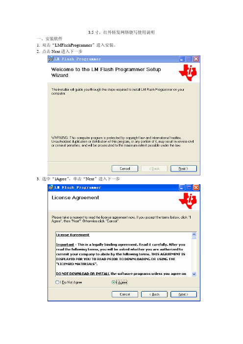
1. 双击“LMFlashProgrammer”进入安装。
2. 点击Next进入下一步
3. 选中“lAgree”,单击“Next”进入下一步
4. 在Folder一栏单击“Browse…”选择程序安装目录后,单击“Next”进入下一步
5. 单击“Next”进入下一步
6. 程序安装中
7. 安装程序完成,单击“Close”退出
二、烧写程序
1. 双击桌面“”图标打开软件
2. 选择“configuration”界面。
2.1. 在“Quick set”一栏复选框里选择“Manual configuration-see below”。
2.2. 在“Interface”一栏复选框里选择“Ethernet”。
2.3. 在“Client IP Address:”后面的框里填上你要烧写的设备的IP地址,如
192.168.0.50。
2.4. “Client MAC Address:”后面的框里填上你要烧写的设备的MAC地址,如
001205071319。
2.5.
3.5寸、红外转发的IP地址与MAC地址都可以通过
获取到。
3. 换到“program”界面
3.1 在“Select.bin file”一栏里,点“browse”选择程序路径。
3.2 单击“Program”烧写
烧写完成后设备会重起。
三、注意事项
1. 设备要与电脑在同一个网段里。
2. 网络烧写时,要用有线连接,不可使用无线连接烧写。
3. 烧写前,3.5寸最好重起一直,重起时不可出现异常现像。
Flash Programmer

Flash Programmer User ManualRev. 1.5Table of contents1INTRODUCTION (3)2ABOUT THIS MANUAL (3)3DEFINITIONS (3)4PROGRAMMING USING THE GUI VERSION (4)4.1S YSTEM ON C HIP (5)4.1.1Device list: (5)4.1.2Actions: (5)4.1.3Flash lock: (6)4.1.4IEEE address / general change field: (6)4.1.5View Info Page (9)4.1.6Updating SmartRF04EB/SmartRF05EB USB MCU firmware (10)4.1.7Updating CC2430DB USB MCU firmware (10)4.2EB BOOTLOADER (11)4.2.1SmartRF04EB (11)4.2.2SmartRF05EB (12)4.3MSP430P ROGRAMMING (13)5COMMAND LINE INTERFACE (14)5.1O PTIONS (14)5.2P LUG-IN TO IAR W ORKBENCH (14)5.2.1Setup (14)5.2.2Use (15)6INSTALLED HEX FILES (18)7DOCUMENT HISTORY (18)1 IntroductionThis is the user manual for the SmartRF Flash Programmer.The Flash Programmer can be used to program the flash memory in Texas Instruments system on chip MCU’s and and for upgrading of the firmware in the USB MCU found on the SmartRF04EB, SmartRF05EB and CC2430DB. In addition the Flash Programmer can be used for programming the flash memory of MSP430 via the MSP-FET430UIF and the eZ430 dongle.When connecting a CC2430EM on SmartRF04EB or a CCMSP2618 on SmartRF05EB, the Flash Programmer also support reading/writing the IEEE address.2 About this manualThis manual covers the use of the Flash programmer, both the GUI version and the command line interface.The intended use of the Flash Programmer is to provide a quick and easy way to download.hex files into Texas Instruments system on chip products. It can also be used to update the firmware on evaluation boards through the USB cable.The manual describes the most common functions and options available. How to access the flash programmer from IAR workbench is also described. Only programming through the USB cable is described. The Flash Programmer also has functionality to program the USB MCU found on SmartRF04EB and CC2430DB through the Silicon Laboratories serial adapter EC2, however this is not covered in this manual.3 DefinitionsSmartRF®04DK A collective term used for all development kits for theSmartRF®04 platform, i.e. CC2510DK and CC2430ZDK SmartRF®05DK A collective term used for all development kits for theSmartRF05 platform, i.e. CC2520DKUSB MCU The Silicon Labs C8051F320 MCU used to provide a USBinterface on the SmartRF®04EB and CC2430DB.The CC2511 MCU used to provide a USB interface on theSmartRF05EB.Factory firmware The firmware that is supplied programmed into the USB MCUfrom the factory. This firmware supports SmartRF® Studiooperation as well as a stand-alone PER tester.GUI Graphical User InterfaceCC Debugger The CC Debugger can be used as interface to program SoC’smounted on Battery Boards and to update the USB MCU onSmartRF05EB.4 Programming using the GUI versionFigure 1: GUI interfaceFigure 1 show the GUI interface of the Flash Programmer. There is five different tab’s to choose from.“System on Chip” is used to program Texas Instruments SOC’s e.g. CC1110, CC2430, CC2510, CC2530. The use of this tab is described in chapter 4.1.“EB application (USB)” is used when updating the USB MCU found on SmartRF04EB, SmartRF05EB, CC Debugger and CC2430DB. The use of this tab is described in chapter Error! Reference source not found..“EB bootlaoder” is used to update the bootlader on SmartRF04EB and SmartRF05EB. Further details are described in chapter 4.3.“MSP430” is used to program the MSP430 MCU used in various RF development kits. Further details are described in chapter 4.4.4.1 System on Chip.list:4.1.1 DeviceThe device list is a list over all currently connected System on Chip devices. Note that when the System on Chip tab is selected, a SmartRF0xEB’s without a System on Chip EM connected will not be displayed.If more than one chip is connected the one selected (marked blue) in this window is the one that will be programmed.4.1.2 Actions:There are five different actions that can be performed on the Texas Instruments SoC’s. To perform an action, select one and then press the “Perform actions” button.The progress bar and output window at the bottom will output the progress and result of the action.The five actions are:Erase and programWill erase the flash memory of the selected SoC and then program it with the .hex file selected in the “Flash image” field.Erase, program and verifySame as “Erase and program”, but after the programming the content of the flash will be read back and compared with the .hex file. This will detect errors during programming or errors caused by damaged flash. It is therefore recommended to always verify afterprogramming.Append and verifyThis action will write the contents of the hex file given in the “Flash image” field, to the selected SoC without erasing the Flash first. Note that all the Flash written to must read 0xFF (be erased) before programming starts. Feature is useful when a program isdivided into more that one hex file.This action uses debug commands to read from the Flash, which means that if thedebug commands are blocked on the chip, it is impossible to perform this action.Verify against hex-fileThis action will compare the contents of the Flash with a .hex file given in the “Flashimage” field.Note that the function only verifies that the contents of the .hex file is present in theFlash, it does not check if there is anything additional written in the Flash.This action uses debug commands to read from the Flash, which means that if thedebug commands are blocked on the chip, it is impossible to perform this action.Read into hex-fileThis action will read the entire content of the Flash and then write it to the hex-file given in the “Flash image” field.Note that the hex-file given in the “Flash image” field will be overwritten.This action uses debug commands to read from the Flash, which means that if thedebug commands are blocked on the chip, it is impossible to perform this action.lock:4.1.3 FlashWhen programming a chip it is possible to apply the different Flash lock and debug command lock that is supported by the chip. These fields will change depending on the chip type selected in the Device list. Please refer to the datasheet for the different chip types for a description of these locks.Note that if the debug command lock is set, it is impossible to use most of the debug commands on the chip. E.g. the Flash may no longer be read out.CC2530:For CC2530 it is possible to write protect each page of the flash image. The input field “Write protect” should be given as shown in Figure 3, Write protect CC2530. The pages to be write protected can be given separated by a comma. It is also possible to specify a range of pages.Figure 3, Write protect CC25304.1.4 IEEE address / general change field:Depending of the chip connected these fields will change.Figure 4: IEEE address for Zigbee SoC (CC2430/31)Figure 5: IEEE address for ZigBee SoC (CC2530/31)Figure 6: Change field for non Zigbee SoCIEEE address on ZigBee devices like CC2430/31On a CC243x the IEEE address is stored in the last 8 bytes of the flash. E.g. the placement is different depending on the size of the Flash. See Table 1 below.Chip type IEEE addressstart IEEE addressendCC243x F-128 0x1FFF8 0x1FFFFCC243x F-64 0xFFF8 0xFFFFCC243x F-32 0x7FF8 0x7FFFTable 1: Placement of IEEE addressTo read the IEEE address from a chip select the appropriate Chip type (e.g. F-128) and push the “Read IEEE” button.To write the IEEE address to a chip, manually write the address into the IEEE field(hexadecimal, with a space between each byte) and then push the “Write IEEEaddress” button.Writing the IEEE address will fail if the flash is write-protected, or the debug command lock is set.If the “Retain IEEE address when reprogramming the chip” is checked the IEEEaddress is preserved when a new program is written to the chip with the “Erase andprogram” or “Erase, program and verify” action. This is however not possible if thedebug command lock is set on the chip before the programming starts.IEEE address on ZigBee devices like CC2530/31For CC253x it is possible to have two IEEE addresses programmed in flash. ThePrimary address is programmed in the Information Page and can only be read. Theaddress is preprogrammed in factory.The secondary IEEE address, which is optional (used when the address in theinformation page is not used), is stored at the end of the flash. The last 16 bytes is used for lock bits and the IEEE address is stored in the last 8 bytes before the lock bits.Chip type IEEE addressstart IEEE addressendCC253x F-256 0x3FFE8 0x3FFEF CC253x F-128 0x1FFE8 0x1FFEF CC253x F-64 0xFFE8 0xFFEF CC253x F-32 0x7FE8 0x7FEFTo read the IEEE address select either Primary or Secondary and push the “ReadIEEE” button.Only the secondary IEEE address can be written. All the other rules are the same as described above for CC243x.Change Field on non ZigBee devicesThe intention of this field is to provide an easy and quick way to give a unique address to the chip when programming it. It gives the user the possibility to change any number of bytes at any location in the program read from the hex file, before it is written to the chip.When “Change” is checked, input the start address, e.g. the first byte that should be changed into the first field.Then the new values are written into the rightmost field (hexadecimal, with a spacebetween each byte)When “Erase and program” or “Erase, program and verify” action is performed, thebytes at the given address from the hex file are replaced with those written by the user before the chip is programmed. The hex file itself is not changed.4.1.5 View Info PageTo view the information page click on the “View Info Page” button shown at the left side (Only applicable for CC253x).The Information Page is a 2 KB read-only region that stores various device information.USB MCU firmware updateFirmwarerevisionnumberFigure 7: USB MCU updateFigure 7 show the “EB application (USB)” tab. It provides the possibility to update the firmware on an Evaluation Board using only a USB cable. No additional programmer is necessary. When a SmartRF04EB, SmartRF05EB, CC Debugger or CC2430DB is connected it will appear in the device list. In the rightmost column the revision number of the current firmware can be read.Note that the update procedure is different for SmartRF04EB and CC2430DB. However the hex file used, (fw400.hex), is identical for the two products.SmartRF05EB uses a different hex file specially build for the USB MCU (CC2511)4.1.6 Updating SmartRF04EB/SmartRF05EB USB MCU firmware1. Remove any CCxxxxEM module and all external equipment connected to theEvaluation Board.2. Connect the USB cable to the Evaluation Board and turn it on, it should appear in theDevice list with “Chip type” N/A.3. Browse to the correct flash image (e.g. srf04eb_fwid0400.hex for SmartRF04EB)4. Choose the “Erase, program and verify”5. Push “Perform actions”.6. The status indicator at the bottom will show the progress and when completed thetext “EB firmware update OK” will appear.4.1.7 Updating CC2430DB USB MCU firmware1. Remove all jumpers on P5.2. Connect pin 9 and 10 on P4 (USB deb) together.3. Connect the USB cable to the CC2430DB and turn it on, it should appear in theDevice list with “Chip type”, “EB type” and “EB firmware ID” set to N/A.4. Browse to the correct flash image (fw400_xx.hex)5. Choose the “Erase, program and verify”6. Push “Perform actions”.7. The status indicator at the bottom will show the progress and when completed thetext “EB firmware update OK” will appear.8. Remove jumper on pin 9-10 on P4, and mount jumpers on P5.Note: After the programming is finished it takes a few seconds before the device appear in the device list. This is due to timing constrains on the USB bus after programming and reset of the device.bootloader4.2 EB4.2.1 SmartRF04EBTo program the bootloader on SmartRF04EB it is required to use the Serial Adapter (EC2) from Silabs.Select Serial port and flash image. The flash image can be selected from a drop down list with a history of the last 10 images that has been programmed. It is also possible to use the button on the right side to browse for the required flash imageSpecify the board identification (ID Number) and select the actions “Erase and program” or “Erase, program and verify”.Click the “Perform actions” button to start programming. Status will be displayed in the field below the button.The action “Verify against hex-file” can be used to check current image on the USB MCU with the given hex file.4.2.2 SmartRF05EBFigure 8, SmartRF05EB bootloaderFor programming of the bootloader on SmartRF05EB, it is possible to use the CC Debugger as illustrated on the image shown when Device SmartRF05EB is selected.It is also possible to use a SmartRF04EB or SmartRF05EB board instead of the CC Debugger. The 10 pin flat ribbon cable should then be connected on the “SoC Debug” header on the SmartRF0xEB.Programmer Device to be programmedFigure 9, Programming of bootloader with SmartRF04EBThe interface speed can be set to either Fast or Slow. This determines the clock speed on the debug interface of the USB MCU. Normally there shouldn’t be any problem to use the fast speed.The flash image can be selected from a drop down list with a history of the last 10 images that has been programmed. It is also possible to use the button on the right side to browse for the required flash image.The connected CC Debugger or SmartRF04EB board should be visible in the list of connected devices. The “Chip type” should be CC2511. Select the required device.Specify the board identification (ID Number) and select the actions “Erase and program” or“Erase, program and verify”.Click the “Perform actions” button to start programming. Status will be displayed in the field below the button.Programming4.3 MSP430Figure 10: MSP430 Programming.Figure 6 show the tab used for programming of the MSP430 MCU. The device can be connected via the USB-Debug-Interface (MSP-FET430UIF) or via the eZ430 USB dongle. Figure 6 show both cases. Devices connected with the MSP-FET430UIF will appear as a COM port. In this case it is COM26. For eZ430 connected devices it will be seen as a HID port. Shown as HID0 in figure 6.When the device is connected via the USB interface, it could take a few seconds before the device appear in the device list.The status of all actions will be given in the Status field at the bottom of the window. An attempt to program a hex file build for another MCU family will be detected and reported in the Status field.The Firmware version of the USB MCU will be checked automatically when a device is connected. If the FW version does not match the MSP430.dll version a message will be given and the user must choose whether or not to update the FW. The update will be performed automatically if the user chooses to update the FW.5 Command Line Interface5.1 OptionsTo get all available options in the command line interface, run the SmartRFProgConsole.exe in a command window or in the IAR workbench without any parameters/arguments. A list of all available options will then be printed out. These options are the same as the ones available in the GUI version of the Flash programmer, please refer to chapter 4 for a description of these.5.2 Plug-in to IAR WorkbenchThe command line interface can be integrated in the IAR Workbench. To setup IAR with this feature follow the instructions below.5.2.1 SetupStart IAR Workbench and choose “Configure Tools…”, from the Tools menu, Figure 11.Figure 11: Tools MenuPress “New”, and add the information present in Table 2, see Figure 12.Field ValueFlashProgramMenuText:Command: C:\Program Files\TexasInstruments\FlashProg\SmartRFProgConsole.exe1Argument: S() EPV F=$TARGET_PATH$ K(0)Table 2: Flash Programmer Setup1 Insert the complete path to the Command Line Flash ProgrammerFigure 12: Configure Tools5.2.2 UseAfter setup, a new target is placed on the Tools menu.Figure 13: Using Flash Programmer from IAR WorkbenchSetup your project to generate hex file as primary output (Figure 15), compile and link, and choose “Flash Program” from the Tools menu. A command line window will be displayed, Figure 14. After the “S” option an empty parenthesize is present. If this parenthesize is empty, the first available development card is used. If more than one development card is connected, fill in the ID number for the card you want to use in the empty parenthesize.The “K(0)” option will retain the IEEE address while programming.Use K(0) on CC2430 F-128, K(1) on CC2430 F-64 and K(2) on CC2430 F-32If the K option is removed the IEEE address is not retained.The “EPV” option is for “Erase, program and verify”Figure 14: Command Line WindowPress OK and the hex file will be downloaded.Figure 15: Generate HEX file as primary outputNote:If the output format is hex file the debugger can not be used.To produce a hex file for banked code, please see the manual named “swru038 IAR User Manual” available from .To have both the hex file and the debug file output, select “Debug information for C-SPY” and “Allow C-SPY-specific extra output file”. Then select the “Extra Output” tab.Select “Generate extra output file” and specify name of the .hex file.6 Installed hex filesAfter installation of the Flash Programmer, a few hex files has also been installed. These can be found on the following directories: C:\Program Files\Texas Instruments\Extras\Srf04Eb and C:\Program Files\Texas Instruments\Extras\Srf05Eb• cc2430db_bootloader.hex Latest version of the CC2430DB bootloader.•srf04eb_fwid0400.hex Latest version of the SmartRF04EB application.•srf04eb_bootloader.hex Latest version of the SmartRF04EB bootloader.•srf05eb_fwid0500.hex Latest version of the SmartRF05EB application.• Srf05eb_bootloader.hex Latest version of the SmartRF05EB bootloader.•Srf05dbg_fwid05CC.hex Latest version of the CC Debugger application.•Srf05dbg_bootloader.hex Latest version of the CC Debugger bootloader.7 Document historyRevision Date Description/Changes1.5 2009-02-11 New version with support for CC2530 andthe CC Debugger.1.4 2007-12-27 New version with support forSmartRF05EB and MSP4301.3 2007-09-19 Update of images and description of hexfiles added.changesMinor1.2 2006-05-16Changedlayout 1.1 2006-02-16release 1.0 2005-12-21InitialIMPORTANT NOTICETexas Instruments Incorporated and its subsidiaries(TI)reserve the right to make corrections,modifications,enhancements,improvements, and other changes to its products and services at any time and to discontinue any product or service without notice.Customers should obtain the latest relevant information before placing orders and should verify that such information is current and complete.All products are sold subject to TI’s terms and conditions of sale supplied at the time of order acknowledgment.TI warrants performance of its hardware products to the specifications applicable at the time of sale in accordance with TI’s standard warranty.Testing and other quality control techniques are used to the extent TI deems necessary to support this warranty.Except where mandated by government requirements,testing of all parameters of each product is not necessarily performed.TI assumes no liability for applications assistance or customer product design.Customers are responsible for their products and applications using TI components.To minimize the risks associated with customer products and applications,customers should provide adequate design and operating safeguards.TI does not warrant or represent that any license,either express or implied,is granted under any TI patent right,copyright,mask work right, or other TI intellectual property right relating to any combination,machine,or process in which TI products or services are rmation published by TI regarding third-party products or services does not constitute a license from TI to use such products or services or a warranty or endorsement e of such information may require a license from a third party under the patents or other intellectual property of the third party,or a license from TI under the patents or other intellectual property of TI.Reproduction of TI information in TI data books or data sheets is permissible only if reproduction is without alteration and is accompanied by all associated warranties,conditions,limitations,and notices.Reproduction of this information with alteration is an unfair and deceptive business practice.TI is not responsible or liable for such altered rmation of third parties may be subject to additional restrictions.Resale of TI products or services with statements different from or beyond the parameters stated by TI for that product or service voids all express and any implied warranties for the associated TI product or service and is an unfair and deceptive business practice.TI is not responsible or liable for any such statements.TI products are not authorized for use in safety-critical applications(such as life support)where a failure of the TI product would reasonably be expected to cause severe personal injury or death,unless officers of the parties have executed an agreement specifically governing such use.Buyers represent that they have all necessary expertise in the safety and regulatory ramifications of their applications,and acknowledge and agree that they are solely responsible for all legal,regulatory and safety-related requirements concerning their products and any use of TI products in such safety-critical applications,notwithstanding any applications-related information or support that may be provided by TI.Further,Buyers must fully indemnify TI and its representatives against any damages arising out of the use of TI products in such safety-critical applications.TI products are neither designed nor intended for use in military/aerospace applications or environments unless the TI products are specifically designated by TI as military-grade or"enhanced plastic."Only products designated by TI as military-grade meet military specifications.Buyers acknowledge and agree that any such use of TI products which TI has not designated as military-grade is solely at the Buyer's risk,and that they are solely responsible for compliance with all legal and regulatory requirements in connection with such use. TI products are neither designed nor intended for use in automotive applications or environments unless the specific TI products are designated by TI as compliant with ISO/TS16949requirements.Buyers acknowledge and agree that,if they use any non-designated products in automotive applications,TI will not be responsible for any failure to meet such requirements.Following are URLs where you can obtain information on other Texas Instruments products and application solutions:Products ApplicationsAmplifiers AudioData Converters AutomotiveDLP®Products BroadbandDSP Digital ControlClocks and Timers MedicalInterface MilitaryLogic Optical NetworkingPower Mgmt SecurityMicrocontrollers TelephonyRFID Video&ImagingRF/IF and ZigBee®Solutions WirelessMailing Address:Texas Instruments,Post Office Box655303,Dallas,Texas75265Copyright©2009,Texas Instruments Incorporated。
flash存储器在线编程

flash存储器在线编程Flash存储器技术趋于成熟,应用广泛,它结合了OTP存储器的成本优势和EEPROM的可再编程性能,是目前比较理想的存储器。
Flash存储器具有电可擦除、无需后备电源来保护数据、可在线编程、存储密度高、低功耗、成本较低等特点。
一般我们都认为Flash储存器具备固有不挥发性、易更新性,可靠性好的基本特性。
从Flash储存器的基本特点可以看出,在单片机中,可以利用F1ash存储器固化程序,一般情况下通过編程器来究成F1ash存储器工作于这种情况,叫监控模式(Monitor mode)或写入器棋式,这与一般的EPROM、0TP、EEPROM装入程序的含义相似。
另一方面,由于Flash存储器具有电可擦除功能,因此,在程序运行过程中,有可能对F1ash存储区的教据或程序进行更新,Flash存储器工作于这种情况,叫用户模式式(User mode)或在线编程模式。
Flash储存器的两种編程模式:1、监控模式或写入器模式2、用户模式或在线编程模式,两种模式各有优缺点:监控模式需要外部硬件支持,但不需要单片机内部程序的存在,所以适合对新出厂芯片进行编程写入,或是对芯片进行整体擦除与写入;用户模式可以在单片机正常工作时进入,所以常用在程序运行过程中对部分Flash存储器的一些单元内容进行修改,特别适合于目标系统的动态程序更新和运行数据的存储。
一般来说,两种模式对Flash存储器的编程操作的程序是一致的,差别在于调用这些程序的方式和环境。
下面我们来详细讲解下Flash储存器在线编程模式对Flash编程的基本操作有两种:擦除(Erase)和写入(Program)。
擦除操作的含义是将存储单元的内容由二进制的0变成1,而写入操作的含义,是将存储单元的内容由二进制的1变成0。
擦除及写入操作都是通过设置或清除Flash存储器的控制寄存器(FLCR)中的某个或某些位来完成的。
Flash命令的执行流程GP32单片机Flash存储器在线编程汇编语言实例首先给出GP32单片机的Flash编程子程序,随后给出在用户模式下进行Flash在线编程的实例,并通过与PC机串行通信方式进。
Flash Programmer使用说明

Flash Programmer使用说明OCD Flash Programmer 是Macraigor 公司专门用于烧写Nor Flash 的在线编程软件可配合Macraigor 所有仿真器的使用。
有支持Windows (非常易于使用)和Linux 2种操作系统的版本。
支持CPU及Flash非常丰富具体可下载OCD Flash Programmer试用版,试用查找。
现在本使用手册以烧写SinoSys-M3 平台为例,结合Macraigor 公司的usb2Demon 仿真器,演示OCD Flash Programmer使用方法。
一、软硬件准备1、硬件SinoSys-M3 是ARM920T CPU采用Samsung S3c2440 ,Flash采用Silicon Stor age Technology的SST39VF1601;仿真器是Macraigor 公司的usb2Demon ARM20 ;PC操作系统是WindowsXp。
2、软件OCD Flash Programmer 正式版;SinoSys-M3 的bootloader.bin ;OCD Commander;二、操作步骤1、安装OCD Commander及OCD Flash Programmer,下载试用版,点击安装即可。
2、将目标板(SinoSys-M3)通过仿真器(usb2Demon)和PC连接起来,给目标板上电。
3、安装usb2Demon 驱动,系统会自动安装该驱动(驱动文件已经包含在步骤1中了),如有疑问,可参见USB2DEMON 使用说明。
4、SinoSys-M3 的bootloader.bin(需要烧写的文件)转化为S19格式。
安装完OCD Flash Programmer 后,会同时安装BinToS19 命令行程序,主要作用是将bin文件转化成S19格式文件,命令格式:即:执行BinToS19.exe bootloader.bin 0X30000000 boot.S19(我是将BinToS19.exe以及bootloader.bin拷贝到同一目录下执行的,执行后会在该目录下生成boot.S19)5、打开OCD Commander设置连接参数如图:6、点击status查看状态是否是in DEBUG:如果不是请点击halt,使其进入调试状态,关闭OCD Commander。
Flash programmer下载指导

Flash programmer下载指导
第一步:
确保机子上安装了Nios II 9.1 Software Build Tools for Eclipse 平台
确保采用的是USB-Blaster下载器(并口下载器无法完成此下载)
确保所下载的文件所在路径目录不含括号
第二步:打开NiosII集成开发环境,选择菜单栏NiosII—>Flash Programmer
第三步:打开后看到如下画面
第四步:新建下载,点击File New……, 弹出第二个对话框“New Flash Programmer Setting File”
第五步:选择SOPC information file name,在对应的工程文件中找到相应的xxx.sopc文件,点击“打开”,然后点击“OK”。
第六步:确认下载线连接是否正确,下载elf文件要将USB下载线接在JTAG模式下载口上,而不是接在AS模式的下载口上
第七步:添加elf文件和sof文件,然后点击右下角的start按钮下载即可,如果下载成功会有相应的信息提示。
SmartRF(TM) Flash Programmer User Manual 中文手册

与eZ430加密狗。
对于IEEE 802.15.4兼容设备(如CC2530的)和蓝牙(R)低能量的装置(例如CC2540)
闪存编程器支持阅读和写作的IEEE MAC地址。
此外,闪存编程器可用于固件升级的SmartRF04EB
SmartRF05EB,CC调试器和CC2430DB。
2关于本手册
本手册涵盖的Flash编程器的使用,两个版本的GUI和命令行
接口。
该手册介绍了最常用的功能和选项。第5.2章将描述如何
使用命令行接口的闪存编程器的IAR Embedded Workbench
执行生成后像闪存编程操作。
Flash编程功能编程的USB MCU上SmartRF04EB
CC2430DB通过Silicon Laboratories的串行适配器EC2的。这是不包括在本手册。
CC243031像ZigBee设备的IEEE地址
在过去的8字节的闪存存储CC243x IEEE地址。例如安置
闪存的大小不同而异。见下文表1。
读取从芯片的IEEE地址,选择合适的芯片类型(如F-128)和推
“读IEEE”按钮。
写芯片的IEEE地址,手动编写成IEEE场(十六进制的地址,
与空间之间的每个字节),然后按下“写入IEEE地址”按钮。
5.1.1.3闪存锁:
当编程的芯片,它可以适用于不同的闪存锁和调试命令锁
芯片支持的选项。根据芯片类型选择,这些领域将改变
设备清单。这些锁的描述,请参阅不同的芯片类型的数据表
功能。
请注意,如果debug命令设置锁定,这是不可能上使用调试命令
芯片。例如闪光灯可能不再被读出。
使用flash programmer软件操作easyarm2200外部flash
R0, =BCFG0 R1, =0x1000ffef R1, [R0]
LDR LDR STR …
R0, =BCFG1 R1, =0x1000ffef R1, [R0]
然后再选择 Flash 标签页进行设置,如图 9 所示。
5
广州周立功单片机发展有限公司 Tel:(020)38730977 38730977 Fax:38730925 设置起始地址 选择小 端模式
广州周立功单片机发展有限公司 Tel:(020)38730977 38730977 Fax:38730925
1.4 结束语
FlashProgrammer 软件还可以对 Flash 器件进行其它的操作,方法类似,在此就不作更 多的描述。用户可以查看软件的帮助文档和以下链接了解更多的信息。
按钮可以读取 Flash 器件的 ID,对话框如图 13 所示。
7
提取 Flash 数据
填充
广州周立功单片机发展有限公司 Tel:(020)38730977 38730977 Fax:38730925
点击
图 13 读取 Flash 器件 ID
按钮可以下载程序至目标板的 Flash 中,编程对话框如图 14 所示。
选择用于下载 的 HEX 文件
选择“编程前 擦空 Flash”
编程按钮在选定 HEX 文件后变实
这些参数不影响 程序下载
图 14 下载程序对话框
在选择 HEX 文件后,灰色的 Program 按钮将变为可用。点击 Program 按钮就可以执行 下载操作,下载结束后的对话框如图 15 所示。
图 15 下载结束对话框 8
选 择 Flash 器件类型 图 9 选择 Flash 标签页进行设置
最后再选择 Program 标签页进行设置,并将设置保存为 EasyARM2200.ocd 文件。
- 1、下载文档前请自行甄别文档内容的完整性,平台不提供额外的编辑、内容补充、找答案等附加服务。
- 2、"仅部分预览"的文档,不可在线预览部分如存在完整性等问题,可反馈申请退款(可完整预览的文档不适用该条件!)。
- 3、如文档侵犯您的权益,请联系客服反馈,我们会尽快为您处理(人工客服工作时间:9:00-18:30)。
SmartRF™ Flash ProgrammerUser ManualSWRU069FTable of contents1INTRODUCTION (3)2ABOUT THIS MANUAL (3)3DEFINITIONS (3)4INSTALLATION. (4)5PROGRAMMING USING THE GUI VERSION (5)5.1P ROGRAM CC XXX S O C OR MSP430 DEVICES. (5)5.1.1System on chip (6)5.1.2MSP430 Programming (11)5.2P ROGRAM E VALUATION B OARD (12)5.2.1USB MCU firmware update (12)5.2.2Automatic Firmware update of the Evaluation Board. (13)5.2.3EB bootloader (15)6COMMAND LINE INTERFACE (17)6.1O PTIONS (17)6.2P LUG-IN TO IAR W ORKBENCH (17)6.2.1Setup (17)6.2.2Use (18)7INSTALLED HEX FILES (21)8DOCUMENT HISTORY (21)This is the user manual for the SmartRF Flash Programmer.The Flash Programmer can be used to program the flash memory in Texas Instruments Low Power RF System on Chips and for programming the flash memory of MSP430 devices via the MSP-FET430UIF and the eZ430 dongle.For IEEE 802.15.4 compliant devices (e.g. CC2530) and Bluetooth® low energy devices (e.g. CC2540) the Flash Programmer support reading and writing the IEEE/MAC address.In addition, the Flash Programmer can be used for upgrading the firmware on the SmartRF04EB, SmartRF05EB, CC Debugger and CC2430DB.2About this manualThis manual covers the use of the Flash programmer, both the GUI version and the -Command Line Interface.The manual describes the most common functions and options available. Chapter 5.2 will describe how to use the Command Line Interface of the Flash Programmer from IAR Embedded Workbench to perform post-build operations like flash programming.The Flash Programmer has functionality to program the USB MCU found on SmartRF04EB andCC2430DB through the Silicon Laboratories serial adapter EC2. This is not covered in this manual.3DefinitionsDownload and unpack the zip file from the TI web page: /tool/flash-programmer Double click on “Setup_SmartRFProgr_x.x.x.exe” file to start the installation. Follow the instructions on the screen.Note:The installation of SmartRF Flash Programmer must be executed with administrator privileges.For Windows Vista and Windows 7 a “User Access Control” dialog will appear when starting the installer. If the user has administrator privileges, click on the “yes” b utton to continue installation. If the user doesn’t have administrator privileges, a user id and password with these privileges must be entered.5 Programming Using the GUI VersionThe Graphical User Interface operates in two different user modes: One for programming of System on Chip modules and one for programming of the Evaluation Boards MCU. 5.1Program CCxxx SoC or MSP430 devices.Figure 1 shows the user mode for programming of System on Chip modules. Two types of modules aresupported.Figure 1, Program CCxxxx SoC or MSP430“System on Chip” is used to program Texas Instruments SOC’s e.g. CC1110, CC2430, CC2510, and CC2530. The use of this tab is described in chapter 5.1.1.“MSP430” is used to program the MSP430 MCU used in various RF development kits. Further details are described in chapter 5.1.2.5.1.1System on chip5.1.1.1 Device list:The device list show all currently connected System on Chip devices. Note that when the System on Chip tab is selected, any Evaluation Board without a System on Chip EM connected will not be displayed.If more than one chip is connected the one selected (marked blue) in this window is the one that will be programmed.There are six different actions that can be performed on the Texas Instruments SoC. To perform an action, select one and then press the “Perform actions” button.The progress bar and output window at the bottom will output the progress and result of the action. The six actions are:EraseThis action will erase the flash memory of the selected SoC.Erase and programWill erase the flash memory of the selected SoC and then program it with the .hex file selected in the“Flash image” field.Erase, program and verifySame as “Erase and program”, but after the programming the content of the flash will be read back and compared with the .hex file. This will detect errors during programming or errors caused by damaged flash. It is therefore recommended to always verify after programming.Append and verifyThis action will write the contents of the hex file given in the “Flash image” field, to the selected SoC without erasing the Flash first. Note that all the Flash written to must read 0xFF (be erased) before programming starts. Feature is useful when a program is divided into more that one hex file.This action uses debug commands to read from the Flash, which means that if the debugcommands are blocked on the chip, it is impossible to perform this action.Verify against hex-fileThis action will compare the contents of the Flash with a .hex file given in the “Flash image” field.Note that the function only verifies that the contents of the .hex file is present in the Flash, it does not check if there is anything additional written in the Flash.This action uses debug commands to read from the Flash, which means that if the debugcommands are blocked on the chip, it is impossible to perform this action.Read into hex-fileThis action will read the entire content of the Flash and then write it to the hex-file given in the “Flash image” field.Note that the hex-file given in the “Flash image” field will be overwritten.This action uses debug commands to read from the Flash, which means that if the debugcommands are blocked on the chip, it is impossible to perform this action.When programming a chip it is possible to apply the different flash lock and debug command lock options that are supported by the chip. These fields will change depending on the chip type selected in the device list. Please refer to the datasheet for the different chip types for a description of these lock features.Note that if the debug command lock is set, it is impossible to use most of the debug commands on the chip. E.g. the flash may no longer be read out.CC11xx, CC25xx and CC24xx:For these devices it is possible to write protect all pages or the upper part of the page numbers.Figure 3, Write protect CC243xCC253x and CC2540:For these devices it is possible to write protect each page of the flash image. The input field “Write protect” should be given as shown in Figure 4, Write protect CC2530. The pages to be write protected can be given separated by a comma. It is also possible to specify a range of pages.Figure 4, Write protect CC25305.1.1.4IEEE 802.15.4 address / general change field:The input fields for the IEEE address depend on the connected RF Device.Figure 5: IEEE address for ZigBee SoC (CC2430/31)Figure 6: IEEE address for ZigBee SoC (CC2530/31)Figure 7: Change field for non ZigBee SoCIEEE address on ZigBee devices like CC2430/31On a CC243x the IEEE address is stored in the last 8 bytes of the flash. E.g. the placement is different depending on the size of the Flash. See Table 1 below.Table 1: Placement of IEEE addressTo read the IEEE address from a chip select the appropriate Chip type (e.g. F-128) and push the “Read IEEE” button.To write the IEEE address to a chip, manually write the address into the IEEE field (hexadecimal, with a space between each byte) and then push the “Write IEEE address” button.Writing the IEEE address will fail if the flash is write-protected, or the debug command lock is set.If the “Retain IEEE address when reprogramming the chip” is checked the IEEE address ispreserved when a new program is written to the chip with the “Erase and program” or “Erase,program and verify” action. This is however not possible if the debug command lock is set on the chip before the programming starts.IEEE address on ZigBee devices like CC2530/31For CC253x it is possible to have two IEEE addresses programmed in flash. The Primary address is programmed in the Information Page and can only be read. The address is preprogrammed in factory.The secondary IEEE address, which is optional (used when the address in the information page is not used), is stored at the end of the flash. The last 16 bytes is used for lock bits and the IEEE address is stored in the last 8 bytes before the lock bits.To read the IEEE address, select either Primary or Secondary and push the “Read IEEE” button.Only the secondary IEEE address can be written. All the other rules are the same as described above for CC243x.Change Field on non ZigBee devicesThe intention of this field is to provide an easy and quick way to give a unique address to the chip when programming it. It gives the user the possibility to change any number of bytes at anylocation in the program read from the hex file, before it is written to the chip.When “Change” is checked, input the start address, e.g. the first byte that should be changed into the first field.Then the new values are written into the rightmost field (hexadecimal, with a space between each byte)When “Erase and program” or “Erase, program and verify” action is performed, the bytes at the given address from the hex file are replaced with those written by the user before the chip isprogrammed. The hex file itself is not changed.5.1.1.5View Information PageTo view the information page click on the “View Info Page” buttonshown at the left side (Only applicable for CC253x and CC254x).The Information Pageis a read-only regionthat stores variousdevice information.5.1.2 MSP430 ProgrammingFigure 8: MSP430 Programming.Figure 8 show the tab used for programming of the MSP430 MCU. The device can be connected via the USB-Debug-Interface (MSP-FET430UIF) or via the eZ430 USB dongle. The figure show both cases. Devices connected with the MSP-FET430UIF will appear as a COM port. In this case it is COM47. For eZ430 connected devices it will be seen as both a HID port and COM port.When the device is connected via the USB interface, it could take a few seconds before the device appear in the device list.The status of all actions will be given in the Status field at the bottom of the window. An attempt to program a hex file build for another MCU family will be detected and reported in the Status field.The Firmware version of the MSP-FET430UIF will be checked automatically when a device isconnected. If the FW version does not match the PC Software version, a message will be given and the user must choose whether or not to update the FW. The update will be performed automatically if the user chooses to update the FW.5.2Program Evaluation BoardFigure 9, Programming of the Evaluation Board“EB application (USB)” is used when updating the USB MCU fo und on SmartRF04EB, SmartRF05EB, CC Debugger and CC2430DB. The use of this tab is described in chapter 5.2.1.“EB application (serial)” can be used in stead of the “EB application (USB)” to update the USB MCU on SmartRF04EB. This setup requires the EC2 serial adapter from Silab. For the rest it has the same functionality as the “EB application (USB)”.“EB bootloader” is used to update the bootloader on SmartRF04EB, SmartRF05EB, CC Debugger and CC2430DB. Further details are described in chapter 5.2.3.5.2.1USB MCU firmware updateFigure 9 show the “EB application (USB)” tab. It provides the possibility to update the firmware on an Evaluation Board using only a USB cable. No additional programmer is necessary. When aSmartRF04EB, SmartRF05EB, CC Debugger or CC2430DB is connected it will appear in the device list. In the rightmost column the revision number of the current firmware can be read.Note that the update procedure is different for SmartRF04EB and CC2430DB. However the hex file used, (fw400.hex), is identical for the two products.SmartRF05EB and CC Debugger uses a different hex file specially build for the USB MCU (CC2511)5.2.1.1Updating SmartRF04EB/SmartRF05EB USB MCU firmware1.Remove any CCxxxxEM module and all external equipment connected to the Evaluation Board.2.Connect the USB cable to the Evaluation Board and turn it on, it should appear in the Devicelist with “Chip type” N/A.3.Browse to the correct flash image (e.g. fw0400.hex for SmartRF04EB)4.Choose the “Erase, program and verify”5.Push “Perform actions”.6.The status indicator at the bottom will show the progress and when completed the text “EBfirmware update OK” will appear.5.2.1.2Updating CC2430DB USB MCU firmware1.Remove all jumpers on P5.2.Connect pin 9 and 10 on P4 (USB deb) together.3.Connect the USB cable to the CC2430DB and turn it on, it should appear in the Device list with“Chip type”, “EB type” and “EB firmware ID” set to N/A.4.Browse to the correct flash image (e.g. fw400.hex)5.Choose the “Erase, program and verify”6.Push “Perform actions”.7.The status indicator at the bottom will show the progress and when completed the text “EBfirmware update OK” will appear.8.Remove jumper on pin 9-10 on P4, and mount jumpers on P5.Note: After the programming is finished it takes a few seconds before the device appear in the device list. This is due to timing constrains on the USB bus after programming and reset of the device.5.2.2Automatic Firmware update of the Evaluation Board.The firmware can be updated automatically with the latest version. The latest version of the firmware is installed together with any of the SmartRF Tools. When the Evaluation Board is connected to the USB port, the flash programmer will compare the current firmware version with the version found in the hex files installed together with the flash programmer. If current firmware is found to be an old version, this will be indicated as shown in Figure 10.Figure 10, Old firmware indicationThere will also be a popup dialog with information about how to update the EB Firmware. See Figure 11Figure 11, Popup dialog for old EB firmware.5.2.3EB bootloaderThe bootloader of the different Evaluation Boards can be updated from the “EB bootloader” tab. 5.2.3.1SmartRF04EBFigure 12, SmartRF04EB BootloaderTo program the bootloader on SmartRF04EB it is required to use the Serial Adapter (EC2) from Silabs.Select Serial port and flash image. The flash image can be selected from a drop down list with a history of the last 10 images that has been programmed. It is also possible to use the button on the right side to browse for the required flash imageSpecify the board identification (ID Number) and select the actions “Erase and program” or “Erase, program and verify”.Click the “Perform actions” button to start programming. Status will be displayed in the field below the button.The acti on “Verify against hex -file” can be used to check current image on the USB MCU with the given hex file.5.2.3.2SmartRF05EBFigure 13, SmartRF05EB bootloaderFor programming of the bootloader on SmartRF05EB, it is possible to use the CC Debugger as illustrated on the image shown when Device SmartRF05EB is selected. It is also possible to use aSmartRF04EB or SmartRF05EB board instead of the CC Debugger. The 10 pin flat ribbon cable should then be connected on the “SoC Debug” header on the SmartRF0xEB.Figure 14, Programming of bootloader with SmartRF04EBThe interface speed can be set to either Fast or Slow. This determines the clock speed on the debug interface of the USB MCU. Normally there shouldn’t be any problem to use the fast speed.The flash image can be selected from a drop down list with a history of the last 10 images that has been programmed. It is also possible to use the button on the right side to browse for the required flash image.The connected CC Debugger or SmartRF04EB board should be visible in the list of connected devices. The “Chip type” should be CC2511. Select the required device.Specify the board identification (ID Number) and select the actions “Erase and program” or “Erase, p rogram and verify”.Click the “Perform actions” button to start programming. Status will be displayed in the field below the button.Programmer Device to be programmed6Command Line Interface6.1OptionsTo get all available options in the command line interface, run the SmartRFProgConsole.exe in a command window without any parameters/arguments. A list of all available options will then be printed out. These options are the same as the ones available in the GUI version of the Flash programmer. Please refer to chapter 4 for a description of these.6.2Plug-in to IAR WorkbenchThe command line interface can be integrated in the IAR Workbench. To setup IAR with this feature follow the instructions below.6.2.1SetupStart IAR Workbench and choose “Configure Tools…”, from the T ools menu, Figure 15.Figure 15: Tools MenuPress “New”, and add the information present in Table 2, see Figure 16.Table 2: Flash Programmer Setup1 Insert the complete path to the Command Line Flash ProgrammerFigure 16: Configure Tools6.2.2UseAfter setup, a new target is placed on the Tools menu.Figure 17: Using Flash Programmer from IAR WorkbenchSetup your project to generate hex file as primary output (Figure 19), compile and link, and choose “Flash Program” from the Tools menu. A command line window will be displayed, Figure 18. After the “S” option an empty parenthesize is present. If this parenthesize is empty, the first available development card is used. If more than one development card is connected, fill in the ID number for the card you want to use in the empty parenthesize.The K(0) option will retain the IEEE address while programming.Use K(0) on CC2430F128, K(1) on CC2430F64 and K(2) on CC2430F32.If the K option is removed the IEEE address is not retained.The “EPV” option is for “Erase, program and verify”Figure 18: Command Line WindowPress OK and the hex file will be downloaded.Figure 19: Generate HEX file as primary outputNote that if you only select the HEX file as output from the linker, you cannot debug this particular image. To have both the hex file and the debug file output, select “Debug information for C-SPY” and “Allow C-SPY-specific extra output file”. Then select the “Extra Output” tab.Select “Generate extra output file” and specify name of the .hex file.SmartRF™ Flash Programmer SWRU069F21/21 7 Installed hex filesAfter installation of the Flash Programmer, a few hex files have been installed. The typical location of these files will be:C:\Program Files\Texas Instruments\SmartRF Tools\FirmwareFor each device there will be a subfolder with the latest firmware version:.\SmartRF04EB \srf04eb_bootloader.hex SmartRF04EB bootloader.\cc2430db_bootloader.hex CC2430DB bootloader\fw0400.hex SmartRF04EB application..\SmartRF05EB \usb_bootloader_srf05eb.hex SmartRF05EB bootloader.\cebal_fw_srf05eb.hex SmartRF05EB application..\CC Debugger \usb_bootloader_srf05dbg.hex CC Debugger bootloader.\cebal_fw_srf05dbg.hex CC Debugger application..\TrxEB \usb_bootloader_trxeb.hex TrxEB bootloader.\cebal_fw_trxeb.hex TrxEB application.8 Document history。