AD404M324RBA-5中文资料
远东M系列阀组使用说明书

阀组系列产品1.VX-32型三阀组2.M364W-420P-35/54型三阀组3.M564W-320P-54五阀组4.EFZ-320C(P)型二阀组5.引压接头VX-32型三阀组使用说明书远东仪表1 用途VX-32型三阀组可与本公司与美国EMERSON TM公司合资生产的1151、3051系列等差压变送器配合使用,其作用是从引压点将信号引入差压变送器正负测量室使引压点与测量室接通或断开。
2 基本参数a. 公称压力: 32MPab. 环境温度: -30℃~+93℃c. 介质温度:≤150℃d. 重量:约2.5kge. 外形尺寸:230×120×180mmf. 材质:1C r18 Ni 9Ti3. 基本结构与工作原理3.1 基本结构(如图1)图 13.2 工作原理M364W型三阀组由两端的引压阀和中间的平衡阀组成,三个阀结构相同,均采用聚四氟乙烯填料和9Cr18阀瓣,通过手柄旋转阀杆可实现阀门的开启与关闭。
关闭二引压阀、打开平衡阀时,正负测量室相通。
打开二引压阀、关闭平衡阀时,两引压管分别与正负测量室相通、两输出端压力不同。
引压阀一开一闭、打开平衡阀时,两输出端压力相同。
4 安装方法将三阀组装有聚四氟乙烯密封圈的二出压孔对准差压变送器法兰侧面1/4ANPT引压孔,均匀旋紧四条螺栓,以保证密封。
5 注意事项本产品出厂前已经打压试验合格,请不要任意松动零件,调整、维护请在专业人员指导下进行。
6 成套性使用说明书 1份检验合格证 1份密封垫圈外径24.5mm径19mm厚2mm 2件螺栓 7/16-20UNF-2A 1″ 4件焊接管接头 2件7. 订货须知根据选用的压力变送器量程代号。
选择三阀组型号(见表)8. 售后服务本产品自发售之日起18个月,在用户完全按使用说明书规定使用的情况下,如出现不符合技术要求的质量问题,我公司负责修理或更换。
M364W-420P-35/54型三阀组使用说明书远东仪表1 用途M364W三阀组可与本公司与美国ROSEMOUNT公司合资生产的1151、3051系列等差压变送器配合使用,其作用是从引压点将信号引入差压变送器正负测量室使引压点与测量室接通或断开。
配电箱型号及规格之欧阳道创编
配电箱规格及参数GCK、GCS、MNS是低压抽出式开关柜;GGD、GDH、PGL是低压固定式开关柜;XZW综合配电箱;ZBW箱式变电站;XL、GXL低压配电柜、建筑工地箱;JXF电器控制箱;PZ20、PZ30系列终端照明配电箱;PZ40、XDD(R)电表计量箱PXT(R)K-□/□-□/□-□/□-□/IP□系列规格型号解释:(1)PXT明装配电箱,暗装加(R)(2)K有如表1的系列配线方式(3)□/□额定电流/额定短时耐受电流能力:用数字表示,250/10表示:额定电流250A/额定短时耐受电流能力10kA,根据顾客要求可以降低。
(4)□/□进线型式:□/1单相输入;□/3三相输入;1/3表示混合输入(5)□×□出线回路:单相回路×三相回路,6×3单相6回路,三相3回路(6)□/ □ 主开关型式/防护等级;1/IP30单相主开关/IP30; 3/IP30三相主开关/IP30表1:序号汉语拼音字头中文解释装配图号电气原理图号1 JL 计量箱 PXT01 PXT01 dq系列2 CZ 插座箱 PXT02 PXT02 dq系列3 ZM 照明箱 PXT03 PXT03 dq系列4 DL 动力箱 PXT04 PXT04 dq系列5 JC 计量插座箱 PXT05 PXT05 dq系列6 JZ 计量照明箱 PXT06 PXT06 dq系列7 JD 计量动力箱 PXT07 PXT07 dq系列8 ZC 照明插座箱 PXT08 PXT08 dq系列9 DC 动力插座箱 PXT09 PXT09 dq系列10 DZ 动力照明箱 PXT10 PXT10 dq系列11 HH 混合功能箱 PXT11 PXT11 dq系列12 ZN 智能箱 PXT12 PXT12 dq系列电气箱柜名称编号规格型号高压开关柜 AH高压计量柜 AM高压配电柜 AA高压电容柜 AJ低压电力配电箱柜 AP低压照明配电箱柜 AL应急电力配电箱柜 APE应急照明配电箱柜 ALE低压负荷开关箱柜 AF低压电容补偿柜 ACC或ACP 直流配电箱柜 AD操作信号箱柜 AS控制屏台箱柜 AC继电保护箱柜 AR计量箱柜 AW励磁箱柜 AE低压漏电断路器箱柜 ARC双电源自动切换箱柜 AT多种电源配电箱柜 AM刀开关箱柜 AK电源插座箱 AX建筑自动化控制器箱 ABC火灾报警控制器箱 AFC设备监控器箱 ABC住户配线箱 ADD信号放大器箱 ATF分配器箱 AVP接线端子箱 AXT举例说明吧GCK第一个 G 代表配电柜第二个 C 代表抽屉式第三个 K 代表控制GGD第一个 G 代表配电柜第二个 G 代表固定式第三个 D 代表动力配电箱1LA1a 1AL1b AT-DT是什么意思还有1AP2 2AP1 3APc 7AP 1KX之类的。
制动单元(4030、4045)最新款-2011
目录第一章综述 ............................................................................................... - 2 -1.1购入检查注意事项 (2)1.2制动单元的型号说明 (2)1.3CDBR系列制动单元的技术条件 (3)1.4CDBR系列制动单元适配制动电阻选用表 (4)第二章安装 ............................................................................................... - 5 -2.1CDBR-4030/4045制动单元的外形尺寸 . (5)2.2制动单元面板安装说明 (6)2.3制动单元的安装方式 (6)第三章接线与运行 ................................................................................... - 8 -3.1接线前的注意事项.. (8)3.2制动单元主回路端子排列 (8)3.3使用说明 (9)第四章面板显示说明 ............................................................................. - 11 -第五章常见故障的排除 ......................................................................... - 12 -第一章综述感谢您使用的CDBR系列制动单元。
CDBR系列制动单元可以把电机调速等过程中产生的再生电能通过制动电阻释放掉,产生足够的制动转矩,保证变频器等设备的正常运行。
CDBR系列制动单元广泛应用于电梯、起重、生产机械、矿山提升机、离心机、油田抽油机等各种场合。
梅兰日兰电气集团苏州有限公司产品手册之MRW1系列智能型万能式低压断路器

梅兰日兰电气集团(苏州)有限公司产品手册之MRW1系列智能型万能式低压断路器1.概述MRW1系列智能型万能式断路器是按最新的标准GB14048. 2的要求推出的新一代智能型万能能式断路器。
产品设计人性化,使用简单,具有全智能、高分断、零飞孤、带隔离、结构紧凑等特点,除具有多功能保护特征外,还具有电流表、电压表、功率因数表、故障检查、自诊断、MCR等多种辅助功能,同时具有通讯接口,可实现远距离的遥控、遥测、遥调、遥讯功能,塑造了新一代断路器的全新形象。
该断路器主要用于控制和保护低压配电网络,一般安装在低压配电柜中作主开关起总保护用,还可以作电动机不频繁起动之用。
产品通过IEC60947-2 (97)国际最新电磁兼容标准和各种型式试验的严格考核,主要技术指标达到国外同类产品的先进水平。
2. 用途及分类①用途MRW1系列智能型万能式断路器(以下简称断路器)适用于交流50Hz,额定电压400V,690V,额定电流为630A-6300A的配电网络中,用来分配电能和保护线路及电源设备免受过载、短路、单相接地、欠电压等的危害。
该断路器具有多种智能保护功能,可做到选择性保护,且动作精确,提高供电可靠性,避免不必要的停电。
同时带有开放式通讯接口,可进行四遥,以满足控制中心和自动化系统的要求。
该断路器在海拔2000M时脉冲耐压8000V(不同海拔按标准修正,最多不超过12000V)。
断路器不带智能控制器及传感器可作隔离器作用,标准为断路器符合G B 1 4 0 4 8 . 2《低压开关设备和控制设备低压断路器》和I EC60947. 2-97《低压开关设备和控制设备低压断路器》等标准。
②分类A、按使用类别分a.非选择性b.选择性B、按安装方式分a.固定式b.抽屉式C、按极数分:三极、四极D、按操作方式分a.电动操作b.手动操作(检修、维护用)③脱扣器种类智能型过电流控制器、欠电压瞬时(或延时)脱扣器、分励脱扣器。
3.正常工作条件①周围空气温度上限值不超过+40℃;下限值不低于-5℃;24h的平均值不超过+35℃;注:a.下限值为-10℃或-25℃的工作条件,在订货时用户须向本公司申明;b.上限值超过+40℃或下限值低于-25℃的工作条件,用户应与本公司协商。
OPA404KU,OPA404KP,OPA404KU 1K,OPA404KU 1KE4,OPA404KUG4,OPA404AG,OPA404BG, 规格书,Datasheet 资料
KP, KU Operating
KP, KU Storage
KP, KU θ Junction-Ambient
KP, KU
IO = 0mADC Ambient Temperature Ambient Temperature Ambient Temperature
© 1986 Burr-Brown Corporation
PDS-677F
Printed in U.S.A. August 1995
芯天下--/
SPECIFICATIONS
ELECTRICAL
At VCC = ±15VDC and TA = +25°C unless otherwise noted.
®
OPA404
2
芯天下--/
ELECTRICAL (FULL TEMPERATURE RANGE SPECIFICATIONS)
At VCC = ±15VDC and TA = TMIN to TMAX unless otherwise noted.
OPA404AG, KP, KU
8
0.5
12
1013 || 1 1014 || 3
±10.5 88 84
+13, –11 100 100
88
100
4
6.4
570
24
35
0.6
1.5
±11.5 +13.2, –13.8
±5
±10
80
1000
±10
±27
±40
±15
±5
±18
9
10
–25
A4504中文资料
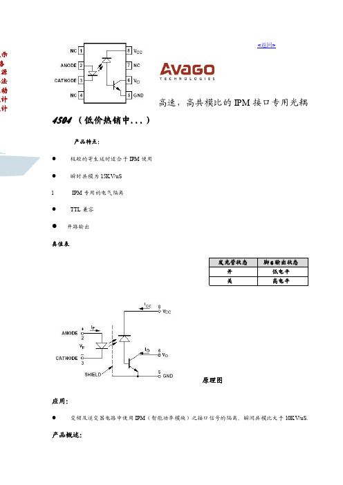
上图是典型的功率器件接口电路以及时序图;
众所周知,当功率管IPM开关工作时,原则上是绝对不能使上下两臂同时导通的。
即使在高下稍有交迭也会潜在威胁功率管和周遍电路,特别是在大电流状态下。
防止这一现象的办法是一只的时候必须确保他的对管已经完全关闭。
在此加入了一段小小的延时,被称之为“死区”。
如何缩是工程师的一项重要的课题。
“开通”IPM延时时间取决于光耦的寄生延时数据又要参照IPM的驱动电路,其中重要的是参大和最小延时时间,上图的LED是输入电压,OUT是输出电压。
大多数设计应用是:当输入为高电打开。
那么根据图上下输入的需要延时的时间至少应该是(tPLHmax-tPHLmin),此数据在手册上大多数情况下,IPM数据手册给定的死区时间是大于光耦所规定的最少要求延时的。
HCPL-4504高速光耦与IPM连接的例图:
设计注意:
1:7脚8脚需要短路连接;
2:IPM功率越大上拉电阻值越小;
3:光耦副边的引线须尽量小于2cm;
1)与DIP-IPM连接原理图:(见DIP-IPM设计手册)
2)与通用IPM连接原理图:
<返回>
上海嘉尚电子科技有限公司版权所有@2005咨询热线:021-********,54420290传真:021-********。
PG5404中文资料

PG5400 THRU PG5408GLASS PASSIVA TED JUNCTION PLASTIC RECTIFIER VOLTAGE - 50 to 1000 Volts CURRENT - 3.0 AmperesFEATURESl Plastic package has Underwriters Laboratory Flammability Classification 94V-O utilizing Flame Retardant Epoxy Molding Compoundl Glass passivated junction in DO-201AD packagel 3.0 ampere operation at T A =55¢J with no thermal runaway l Exceeds environmental standards of MIL-S-19500/228l Low reverse leakage current MECHANICAL DA TA Case: Molded plasticTerminals: Axial leads, solderable per MIL-STD-202, Method 208Mounting Position: Any Weight: 0.04 ounce, 1.1 gramMAXIMUM RA TINGS AND ELECTRICAL CHARACTERISTICS Ratings at 25¢J ambient temperature unless otherwise specified.Single phase, half wave, 60 Hz, resistive or inductive load.For capacitive load, derate current by 20%.PG5400PG5401PG5402PG5404PG5406PG5407PG5408UNITSMaximum Recurrent Peak Reverse Voltage501002004006008001000V Maximum RMS Voltage3570140280420560700V Maximum DC Blocking Voltage501002004006008001000V Maximum Average Forward Rectified Current .375"(9.5mm) lead length at T A =55¢J3.0APeak Forward Surge Current, 8.3ms single half sine-wave superimposed on rated load(JEDEC method)150A Maximum Forward Voltage at 3.0A1.2V Maximum Reverse Current at T a =25¢J At Rated DC Blocking Voltage T a =100¢J5.0100£g A £g A Typical Junction capacitance (Note 1)30P F Typical Thermal Resistance R £K JA(Note 2)20¢J /W Typical Reverse Recovery Time(Note 3)2£g S Operating and Storage T emperature Range T A-55 to +150¢JNOTES:1. Measured at 1 MHz and applied reverse voltage of 4.0 VDC2. Thermal resistance from junction to ambient and from junction to lead at 0.375”(9.5mm) lead length P.C.B mounted3. Reverse Recovery T est Conditions: I F =.5A, I R =1A, Irr=2.5ADO-201ADRATING AND CHARACTERISTIC CURVES PG5400 THRU PG5408PERCENT OF RATED PEAK REVERSE VOLTAGEAMBIENT TEMPERATURE, ¢JFig. 1-TYPICAL REVERSE CHARACTERISTICS Fig. 2-FORWARD DERATING CURVEAMBIENT TEMPERATURE, ¢JMAXIMUM FORWARD VOLTAGE-VFM(VpK)Fig. 3-FORWARD CURRENT DERATING CURVE Fig. 4-TYPICAL JUNCTION CAPACITANCENO. OF CYCLES AT 60HzFig. 5-MAXIMUM OVERLOAD SURGE CURRENT。
MBR4045中文资料
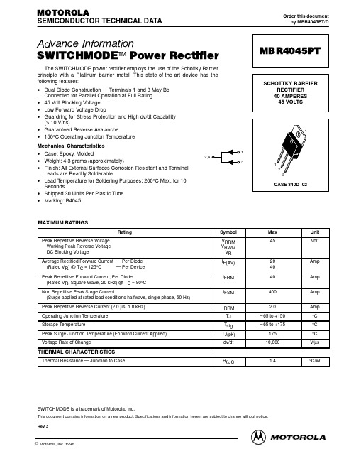
C, CAPACITANCE (pF)
1000
100
1
10 VR, REVERSE VOLTAGE (VOLTS)
100
110
120 130 140 TC, CASE TEMPERATURE (°C)
150
160
Figure 3. Typical Capacitance Per Leg
Figure 4. Current Derating Per Leg
TC = 25°C
TC = 100°C 1 100
TC = 25°C 800 0.01 0 10 20 30 VR, REVERSE VOLTAGE (VOLTS) 40 50
200 300 400 500 600 700 vF, INSTANTANEOUS FORWARD VOLTAGE (mV)
3
元器件交易网 MBR4045PT
Motorola reserves the right to make changes without further notice to any products herein. Motorola makes no warranty, representation or guarantee regarding the suitability of its products for any particular purpose, nor does Motorola assume any liability arising out of the application or use of any product or circuit, and specifically disclaims any and all liability, including without limitation consequential or incidental damages. “Typical” parameters which may be provided in Motorola data sheets and/or specifications can and do vary in different applications and actual performance may vary over time. All operating parameters, including “Typicals” must be validated for each customer application by customer’s technical experts. Motorola does not convey any license under its patent rights nor the rights of others. Motorola products are not designed, intended, or authorized for use as components in systems intended for surgical implant into the body, or other applications intended to support or sustain life, or for any other application in which the failure of the Motorola product could create a situation where personal injury or death may occur. Should Buyer purchase or use Motorola products for any such unintended or unauthorized application, Buyer shall indemnify and hold Motorola and its officers, employees, subsidiaries, affiliates, and distributors harmless against all claims, costs, damages, and expenses, and reasonable attorney fees arising out of, directly or indirectly, any claim of personal injury or death associated with such unintended or unauthorized use, even if such claim alleges that Motorola was negligent regarding the design or manufacture of the part. Motorola and are registered trademarks of Motorola, Inc. Motorola, Inc. is an Equal Opportunity/Affirmative Action Employer. Mfax is a trademark of Motorola, Inc. How to reach us: USA / EUROPE / Locations Not Listed: Motorola Literature Distribution; P.O. Box 5405, Denver, Colorado 80217. 1–303–675–2140 or 1–800–441–2447 Customer Focus Center: 1–800–521–6274 Mfax™: RMFAX0@ – TOUCHTONE 1–602–244–6609 ASIA/PACIFIC: Motorola Semiconductors H.K. Ltd.; 8B Tai Ping Industrial Park, Motorola Fax Back System – US & Canada ONLY 1–800–774–1848 51 Ting Kok Road, Tai Po, N.T., Hong Kong. 852–26629298 – /mfax/ HOME PAGE: /sps/ JAPAN: Nippon Motorola Ltd.: SPD, Strategic Planning Office, 4–32–1, Nishi–Gotanda, Shinagawa–ku, Tokyo 141, Japan. 81–3–5487–8488
- 1、下载文档前请自行甄别文档内容的完整性,平台不提供额外的编辑、内容补充、找答案等附加服务。
- 2、"仅部分预览"的文档,不可在线预览部分如存在完整性等问题,可反馈申请退款(可完整预览的文档不适用该条件!)。
- 3、如文档侵犯您的权益,请联系客服反馈,我们会尽快为您处理(人工客服工作时间:9:00-18:30)。
ASCEND Semiconductor 4Mx4 EDO Data sheetDescriptionThe device CMOS Dynamic RAM organized as 4,194,304 words x 4 bits with extended data out access mode. It is fabricated with an advanced submicron CMOS technology and designed to operate from a single 3.3V oniy power supply. Low voltage operation is more suitable to be used on battery backup, portable elec-tronic application. lt is packaged in JEDEC standard 26/24-pin plastic SOJ or TSOP(II).Features• Single 3.3V(%) only power supply • High speed t RAC acess time: 50/60ns • Low power dissipation- Active mode : 432/396 mW (Mas) - Standby mode: 0.54 mW (Mas)• Extended - data - out(EDO) page mode access • I/O level: CMOS level (Vcc = 3.3V)• 2048 refresh cycle in 32 ms(Std.) or 128 ms(S-version)• 4 refresh modesh: - RAS only refresh- CAS - before - RAS refresh - Hidden refresh - Self-refresh(S-version)10±Pin Name FunctionA0-A10Address inputs- Row address - Column address - Refresh address DQ1~DQ4Data-in / data-out RAS Row address strobe CAS Column address strobe WE Write enable OE Output enable Vcc Power (+ 3.3V)VssGroundVCC 1DQ12DQ23DQ34DQ45VCC6891011 NC 12 WE 13A0 A117 A218 A319VSS RAS CAS OE A8A7A6A5A4VSSAD404M42VSPin Description Pin Configuration21222324 2526151416 A1026/24-PIN 300mil Plastic SOJA9VCC 1DQ12DQ23DQ34DQ45VCC6891011 NC 12 WE 13A0 A117 A218 A319VSS RAS CAS OE A8A7 A6A5 A4VSSAD404M42VT212223242526151416 A1026/24-PIN 300mil Plastic TSOP (ll)A9A0-A10A0-A10A0-A10WECASNO. 2 CLOCK GENERATORCOLUMN ADDRESS BUFFERS (11)REFRESH CONTROLLERREFRESH COUNTERBUFFERS (11)ADDRESS ROW NO. 1 CLOCK GENERATORA0RASA1A2A3A4A5A6A7A8CONTROLLOGICDATA-IN BUFFERDATA-OUT BUFFEROEDQ1.DQ4.COLUMN DECODER2048SENSE AMPLIFIERSI/O GATING2048x42048x2048x4MEMORY ARRAY2048R O W D E C O D E RVcc VssBlock DiagramA9A10TRUTH TABLENotes: 1. EARLY WRITE only.FUNCTIONRASCAS WE OE ADDRESSESDQ SNotesROW COL STANDBY H X X X X High-Z READL L H L ROW COL Data-Out WRITE: (EARLY WRITE )L L L X ROW COL Data-lnREAD WRITE L L ROW COL Data-Out,Data-ln EDO-PAGE-MODE READ1st Cycle L H L ROW COL Data-Out 2nd CycleL H L n/a COL Data-Out EDO-PAGE MODE WRITE1st CycleL L X ROW COL Data-In 2nd Cycle L L Xn/a COL Data-InEDO-PAGE-MODEREAD-WRITE 1st Cycle L ROW COL Data-Out, Data-In 2nd Cycle L n/a COL Data-Out, Data-In HIDDEN REFRESHREAD L H L ROW COL Data-Out WRITEL L X ROW COL Data-In 1RAS-ONLY REFRESH L H X X ROW n/a High-Z CBR REFRESHLHXXXHigh-ZH X →H L →L H →H L →H L →H L →H L →H L →H L →L H →H L →H L →L H→L H L →→L H L→→H L→Absolute Maximum RatingsRecommended DC Operating ConditionsCapacitanceTa = 25°C, V CC = 3.3V%, f = 1MHz Note: 1. Capacitance measured with effective capacitance measuring method. 2. RAS, CAS = V IH to disable Dout.ParameterSymbol Value Unit Voltage on any pin relative to Vss V T -0.5 to + 4.6V Supply voltage relative to Vss V CC -0.5 to + 4.6V Short circuit output current I OUT 50mA Power dissipation P D 1.0WOperating temperature T OPT 0 to + 70°C Storage temperatureT STG-55 to + 125°CParameter/Condition Symbol3.3 Volt VersionUnitMinTyp MaxSupply VoltageV CC 3.0 3.33.6V Input High Voltage, all inputs V IH 2.0-V CC + 0.3V Input Low Voltage, all inputsV IL-0.3-0.8VParameterSymbol Typ Max Unit Note Input capacitance (Address)C I1 -5pF 1Input capacitance (RAS, CAS, OE, WE)C I2-7pF 1Output capacitance(Data-in, Data-out)C I/O-7pF1, 210±DC Characteristics :(T a = 0 to 70°C, V CC = + 3.3V%, V SS = 0V)Parameter Symbol Test Conditions AD404M42V Unit Notes-5-6Min Max Min MaxOperating current I CC1RAS cyclingCAS, cyclingt RC = min-120-110mA1, 2Standby Current LowpowerS-versionI CC2LVTTL interfaceRAS, CAS = V IHDout = High-Z-0.5-0.5mACMOS interfaceRAS, -0.2VDout = High-Z-0.15-0.15mAStandardpowerversionLVTTL interfaceRAS, CAS = V IHDout = High-Z-2-2mACMOS interfaceRAS,-0.2VDout = High-Z-0.5-0.5mARAS- only refresh current I CC3RAS cycling, CAS = V IHt RC = min-120-110mA1, 2 EDO page mode current I CC4t PC = min-90-80mA1, 3CAS- before- RAS refresh current I CC5t RC = minRAS, CAS cycling-120-110mA1, 2Self- refresh current (S-Version)I CC8 - 550 - 55010±CAS V CC≥CAS V CC≥t RASS100µs≥µADC Characteristics :(T a = 0 to 70°C , V CC = +3.3V %, V SS = 0V)Notes:1. I CC is specified as an average current. It depends on output loading condition and cycle rate when the device is selected. I CC max is specified at the output open condition.2. Address can be changed once or less while RAS = V IL .3. For I CC4, address can be changed once or less within one EDO page mode cycle time.Parameter Symbol Test Conditions AD404M42VUnitNotes-5-6Min MaxMin MaxInput leakage current I LI + 0.3V -55-55Output leakage current I LO + 0.3V Dout = Disable -55-55Output high Voltage V OH I OH = -2mA 2.4- 2.4-V Output low voltage V OLI OL = +2mA-0.4-0.4V10±0V Vin V CC ≤≤µA 0V Vout V CC ≤≤µAAC Characteristics(T a = 0 to + 70°C , V cc = 3.3V %, V ss = 0V) *1, *2, *3, *4Test conditions• Output load: one TTL Load and 100pF (V CC = 3.3V %)• Input timing reference levels:V IH = 2.0V, V IL = 0.8V (V CC = 3.3V %)• Output timing reference levels:V OH = 2.0V, V OL = 0.8V10±10±10±Read, Write, Read- Modify- Write and Refresh Cycles (Common Parameters)ParameterSymbol AD404M42V UnitNotes-5-6Min MaxMin MaxRandom read or write cycle time t RC 84-104-ns RAS precharge timet RP 30-40-ns CAS precharge time in normal mode t CPN 10-10-ns RAS pulse width t RAS 50100006010000ns 5CAS pulse width t CAS 8100001010000ns 6Row address setup time t ASR 0-0-ns Row address hold time t RAH 8-10-ns Column address setup time t ASC 0-0-ns 7Column address hold time t CAH 8-10-ns RAS to CAS delay timet RCD 12371445ns 8RAS to column address delay time t RAD 10251230ns 9Column address to RAS lead time t RAL 25-30-ns RAS hold time t RSH 8-10-ns CAS hold timet CSH 38-40-ns CAS to RAS precharge time t CRP 5-5-ns 10OE to Din delay time t OED 12-15-ns Transition time (rise and fall)t T 150150ns 11Refresh periodt REF -32-32ms Refresh period (S- Version)t REF -128-128ms CAS to output in Low- Z t CLZ 0-0-ns CAS delay time from Din t DZC 0-0-ns OE delay time from Dint DZO-0-nsRead CycleWrite Cycle Parameter SymbolAD404M42V Unit Notes-5-6Min Max Min MaxAccess time from RAS t RAC-50-60ns12 Access time from CAS t CAC-14-15ns13, 14 Access time from column address t AA-25-30ns14, 15 Access time from OE t OEA-12-15nsRead command setup time t RCS0-0-ns7 Read command hold time to CAS t RCH0-0-ns10, 16 Read command hold time to RAS t RRH0-0-ns16 Output buffer turn-off time t OFF012015ns17 Output buffer turn-off time from OE t OEZ012015ns17Parameter SymbolAD404M42V Unit Notes -5-6Min Max Min MaxWrite command setup time t WCS0-0-ns7, 18 Write command hold time t WCH8-10-nsWrite command pulse width t WP8-10-nsWrite command to RAS lead time t RWL13-15-nsWrite command to CAS lead time t CWL8-10-nsData-in setup time t DS0-0-ns19 Data-in hold time t DH8-10-ns19 WE to Data-in delay t WED10-10-nsRead- Modify- Write CycleRefresh Cycle Parameter SymbolAD404M42V Unit Notes-5-6Min Max Min MaxRead-modify- write cycle time t RWC108-133-nsRAS to WE delay time t RWD64-77-ns18 CAS to WE dealy time t CWD26-32-ns18 Column address to WE delay time t AWD39-47-ns18 OE hold time from WE t OEH8-10-nsParameter SymbolAD404M42VUnit Notes -5-6Min Max Min MaxCAS setup time (CBR refresh) t CSR5-5-nsCAS hold time (CBR refresh)t CHR8-10-ns10 RAS precharge to CAS hold time t RPC5-5-ns7 RAS pulse width (self refresh)t RASS100-100-RAS precharge time (self refresh)t RPS90-110-nsCAS hold time (CBR self refresh)t CHS-50--50-nsWE setup time t WSR0-0-nsWE hold time t WHR10-10-nsµsEDO Page Mode CycleEDO Page Mode Read Modify Write CycleParameterSymbol AD404M42VUnit Notes-5-6Min MaxMin MaxEDO page mode cycle timet PC 20-25-ns EDO page mode CAS precharge time t CP 10-10-ns EDO page mode RAS pulse width t RASP 5010560105ns 20Access time from CAS precharge t CPA -30-35ns 10, 14RAS hold time from CAS precharge t CPRH 30-35-ns OE high hold time from CAS high t OEHC 5-5-ns OE high pulse widtht OEP 10-10-ns Data output hold time after CAS low t COH 5-5-ns Output disable delay from WEt WHZ 310310ns WE pulse width for output disable whenCAS hight WPZ7-7-nsParameterSymbol AD404M42V Unit Notes -5-6Min MaxMin MaxEDO page mode read- modify- write cycle CAS precharge to WE delay timet CPW 45-55-ns 10EDO page mode read- modify- write cycle timet PRWC56-68-nsNotes :1. AC measurements assume t T = 2ns.2. An initial pause of 100 is required after power up, and it followed by a minimum of eightinitialization cycles (RAS - only refresh cycle or CAS - before - RAS refresh cycle). If the internal refresh counter is used, a minimun of eight CAS - before - RAS refresh cycles are required.3. In delayed write or read-modify-write cycles, OE must disable output buffer prior to applying data to the device.4. All the V CC and V SS pins shall be supplied with the same voltages.5. t RAS (min) = t RWD (min)+t RWL (min)+t T in read-modify-write cycle.6. t CAS (min) = t CWD (min)+t CWL (min)+t T in read-modify-write cycle.7. t ASC (min), t RCS (min), t WCS (min), and t RPC are determined by the falling edge of CAS .8. t RCD (max) is specified as a reference point only, and t RAC (max) can be met with the t RCD (max) limit.Otherwise, t RAC is controlled exclusively by t CAC if t RCD is greater than the specified t RCD (max) limit. 9. t RAD (max) is specified as a reference point only, and t RAC (max) can be met with the t RAD (max) limit.Otherwise, t RAC is controlled exclusively by t AA if t RAD is greater than the specified t RAD (max) limit. 10. t CRP , t CHR , t RCH , t CPA and t CPW are determined by the rising edge of CAS .11. V IH (min) and V IL (max) are reference levels for measuring timing or input signals. Therefore, transitiontime is measured between V IH and V IL .12. Assumes that t RCD tRCD (max) and t RAD t RAD (max). If t RCD or t RAD is greater than the maximum recommended value shown in this table, t RAC exceeds the value shown. 13. Assumes that (max) and (max).14. Access time is determined by the maximum of t AA , t CAC , t CPA . 15. Assumes that (max) and (max). 16. Either t RCH or t RRH must be satisfied for a read cycle.17. t OFF (max) and t OEZ (max) define the time at which the output achieves the open circuit condition (highimpedance). t OFF is determined by the later rising edge of RAS or CAS.18. t WCS , t RWD , t CWD , and t AWD are not restrictive operating parameters. They are included in the datasheet as electrical characteristics only. If (min), the cycle is an early write cycle and the data out will remain open circuit (high impedance) throughout the entire cycle. If (min),(min), (min) and (min), the cycle is a read-modify-write and the data output will contain data read from the selected cell. If neither of the above sets of conditions is satisfied, the condition of the data output (at access time) is indeterminate.19. These parameters are referenced to CAS separately in an early write cycle and to WE edge in adelayed write or a read-modify-write cycle.20. t RASP defines RAS pulse width in EDO page mode cycles.µs ≤≤t RCD t RCD ≥t RADt RAD ≤t RCD t RCD ≤t RAD t RAD ≥t WCS t WCS ≥t RWD t RWD ≥t CWDt CWD ≥t AWD t AWD ≥t CPW t CPW≥Timing Waveforms• Read Cyclet RC t RASt RPtCRPtCPNtRRHtRCHt OEZ t OFF tOEA tCACt AAtRACt CLZD OUTtRCS t ASR tRAH tASC tCAH tRAD t RALtCAStRSH tRCDt TtCSHRASCASADDRESSWEDQ1~DQ4Note : = don’t care OEt OFFRowColumn= Invalid Dout•Early Write CycletRC t RASt RPt WCHt DSt DHt WCS t RALtCAStRSH tRCDt TtCSHRASCASWEDQ1~DQ4tCRPtASRtRAH tASCtCAH ADDRESSColumnRowtCPND INtRADt RAL• Delayed Write CycletRC t RASt RPt RWL t RCSt CAStRSH tRCDt TtCSHRASCAStASR tRAH tCAHADDRESSColumnRow tASC D INDQ1~DQ4WEtCRPtCPNt DHt DSt OEHt OEDOEt DSOPENt WPt CWL• Read - Modify - Write CycletRWC t RASt RPtRWDt WPtRADtRWL tCAStCWL tRCDt TtCPNRASCASWEtCRP t ASRtRAHtASCtCAHADDRESS Column RowDQ1~DQ4t DHt DSOEtRCStAWD tCWD D INt OEDt OEHt OEZt OEA t CAC t RACt AADQ1~DQ4D OUTOPENtDZCtDZO• EDO Page Mode Read CycletRASPtCPRHt RCStCAStRSH tRCDt OEAtCSHRASCAStASRtRAHtCAHADDRESStCASWEtCRPt CPOEDQ1~DQ4OPENtOEPD OUT 1t PCt CPtCAStCPNtCRPtRADtCAHtASCt ASCtCAHt ASCt RAL Row Column 1t OEAt OEHCtRRH tRCHt RACt AAt AAt AA t CPA t CPA t OEZt OFFt OFFt CACt OEZt CAC t CACt COHD OUT NWE OE Column 2Column N Rowt RPD OUT 2• EDO Page Mode Early Write CycletRASPtRPt WCSt CAStRSH tRCDRASCAStASRtRAHtCAHADDRESStCASWEt CPDQ1~DQ4t PCt CPt CAStCPNtCRP tCAH tASCtASC tCAH tASC Row Column 1t DS WE Column 2Column Nt WCH t WCS t WCH t WCS t WCHt DH t DS t DH t DS t DHD IN 1D IN 2D IN Nt TtCSH• EDO Page Mode Read-Early-Write Cyclet RASPtCPRHt RCStCAStRSH tRCDt OEAtCSHRASCAStASRtRAHtCAHADDRESStCASWEtCRPt CPOEDQ1~DQ4OPENtWEDt PCt CPtCAStCPNtCRPtRADtRAHtASCt ASCtCAHt ASCt RAL Row Column 1tWCStRCHt RACt AAt AAt CPA t DHt WHZt CACt CACt COHWE OE Column 2Column N Rowt RPt CAL tWCHDataDoutput 2Data Input NDataDoutput 1t DStCSH• EDO Page Mode Read-Modify-Write Cyclet RASPt CPRHt RCStCASt WP RASCASt ASRtRAHtCAHADDRESSt CASWEtRCDCPDQ1~DQ4tPRWCt CPtCAStCRPtRADtCAHtASCt ASCtCAH tASC Row Column 1tRWLtRCSt OEDt DZOt CAC WE OEt RPt RAL D OUT 2D OUT ND OUT 1tTt Column NColumn 2Column 1tRWD tAWD tCWDtCWLtRCStCWDtAWD tCPW tCWL tCPW tAWD tCWDtCWL t OEDt OEDt OEHt OEHt OEHt CAC t CAC t OEA t AAt RACt OEZt OEAt AA t CPAt OEZt OEAt AA t CPAt OEZ t DSt DHt WP t DSt DHt WP t DSt DHOPENOPENOPEN D IN 1D IN ND IN 2DQ1~DQ4t DZCt DZOt DZCt DZCt DZO• Read Cycle with WE Controlled Disablet WPZt RCStCAStRCDt TtCSHRASCASt ASRtRAHtCAHADDRESSColumnRow tASCD DQ1~DQ4WEt OEZt DSt WHZOEt RCH t OEA t CACt AAt RACt CLZOUTtRADRASADDRESSt RC t CRPt ASRt RAHt Tt RPCROWt OFFCAS t RASt RPOPENt CRPDQ1~DQ4RASt CSRt WSRt RPt T t RPCt OFFCAS t RASt RPOPENt CRPDQ1~DQ4t RPCt CHRt RASt RPt RCt RCt CHRt CSRt WHRt WSRt WHRWECAS-Before-RAS Refresh CycleRASWEt RPCt OFFt CSRt CHSt WSRCASt RASS t RPSOPENDQ1~DQ4t WHRHigh lmpedance• Hidden Refresh Cyclet RPt RASRASt RCDt CRPADDRESSWEt CHRt CASt RSHt RAHt ASRt ASCt CAHt RAL ROW t RCHt OEZCASDQ1~DQ4t Tt RCSD t RASt RASt RPt RPt RC t RCt RCt RADt RRHt OFF t OFFt OEA t CACt AAt RACCOlumnOUTOE(READ)(REFRESH)(REFRESH)Ordering informationAD404M42VSA-5• AD• Ascend Memory Product • 40 • Device Type• 4M4 • Density and Organization • 2• Refresh Rate, 2: 2K Refresh • V• T: 5V, V: 3.3V• S • Package Type (S : SOJ, T : TSOP II)• A• Version• 5• Speed (5: 50 ns, 6: 60 ns)Part Number Access time PackageAD404M42VSA-5AD404M42VSA-6AD404M42VTA-5AD404M42VTA-650 ns 60 ns 50 ns 60 ns300mil 26/24-Pin Plastic SOJTSOP IIPackaging information • 300 mil, 26/24-Pin Plastic SOJ• 300 mil, 26/24-Pin TSOP II。