MRF6S9045NR1中文资料
PCB封装库 建库规则
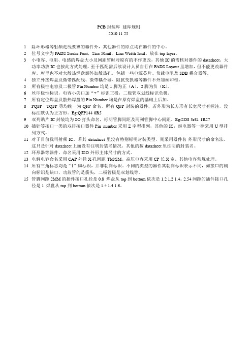
PCB封装库建库规则2010 11 251除环形器等射频走线要求的器件外,其他器件的原点均在器件的中心。
2位号文字为PADS Stroke Font,Size 50mil,Line Width 5mil。
放在top layer。
3小电容、电阻、电感的焊盘大小及间距暂时对原有的不作更改,其他IC的需核对器件的datasheet。
大功率功放IC也按此方式处理,至于匹配需后续设计人员自行在PADS Layout里增加,但不能更改器件库。
库里也不对大散热焊盘额外加散热孔,包括一些电源芯片、负载电阻及3DB耦合器等。
4独立外接焊盘及微带匹配线、微带耦合器、阻抗变换器等器件不外加丝印框。
5所有极性电容及二极管Pin Number均是1脚为正(A),2脚为负(K)。
6丝印极性标识,电容小尖口加“+”标识正极,二极管双划线标识负极。
7所有定位焊盘及散热焊盘的Pin Number均是在原有焊盘的基础上后加。
8PQFP TQFP等均统一为QFP命名,所有QFP封装的器件,若外形为长方形有长宽尺寸有标注,没标注默认为正方形。
Eg:QFP144-0R59双列贴片IC封装均为SO打头命名,标明管脚间距及两列管脚中心间距。
Eg:SO8-3r81-1R2710插针等接口一类的双排接口器件Pin number采用Z字型排列,其他的IC,继电器等一律采用U型排列方式。
11对于目前我司射频IC,若其datasheet里没有特别标明封装类型,则采用器件名-外形尺寸的命名法。
这只是针对datasheet上面没有注明封装名情况。
其他的按datasheet里注明的封装名。
12环形器等器件,命名采用ISO-外形主体尺寸的方式。
13电解电容命名采用CAP外径X孔间距-TM/SM。
高压电容采用CP长X宽。
其他电容常规处理。
14所有三角标志均是“1”脚标识,并非朝向标识。
不同的类型的器件其朝向标识表示不同,如接口的朝向标识是缺口,功放管的是箭头,二极管极是双划线等。
n45磁铁参数
n45磁铁参数N45磁铁是一种高性能永磁材料,它也被称为钕铁硼磁铁。
它是由稀土元素钕(Nd)、铁(Fe)和硼(B)混合制成的。
N45磁铁的磁化能力非常强,可以在室温下保持高达1.4特斯拉的磁场强度。
这种高磁场强度意味着N45磁铁可以产生很大的吸力,并且在许多应用中非常有用。
N45磁铁的其他重要参数包括磁滞回线、矫顽力、矫顽力温度系数和热稳定性等,这些参数对于应用中的性能至关重要。
磁滞回线是磁化过程中的一个重要参数,它表示材料磁化程度的变化。
在常规应用中,磁滞回线不应该太大,因为这会导致磁场强度不够均匀,影响磁铁的性能。
对于N45磁铁,其磁滞回线小于1.1 kG。
矫顽力是另一个重要的磁铁参数,它表示对磁铁进行磁场矫正所需的场强大小。
通常,矫顽力越大,磁铁的磁化能力越强。
N45磁铁的矫顽力为50 kOe。
矫顽力温度系数是一个体现磁铁性能稳定性的参数,它表示磁铁的磁化能力在不同温度下的变化。
对于N45磁铁,其矫顽力温度系数约为-0.11%/℃。
热稳定性是另一个与磁铁性能相关的参数。
对于N45磁铁,在高温下仍然能够保持很高的磁场强度和磁性能,在室温下的磁场几乎不会衰减。
这种热稳定性使得N45磁铁非常适合在高温环境下使用。
N45磁铁是一种高性能永磁材料,具有非常强的磁化能力和热稳定性。
了解其相关参数对于选择合适的磁铁应用非常重要。
除了上述参数,N45磁铁的外观形状和尺寸也是应用中需要考虑的因素。
N45磁铁可以制成各种形状,包括圆柱形、方形、圆盘形、环形等等。
N45磁铁的尺寸也可以根据具体应用需求定制,以满足不同场合的要求。
在各种应用中,N45磁铁都能够发挥出其优异的磁性能与吸力。
最常见的应用包括:电机、发电机、传感器、医疗设备、航空航天、汽车、电子设备等。
在电机、发电机等领域中,N45磁铁被广泛用于永磁同步电机、直流电机等方面。
在传感器方面,N45磁铁可以作为位移传感器、角位移传感器、速度传感器、磁场传感器和探测器等等。
AS9025资料

Cooper-WheelockAS/AH SeriesSingle & Multi-Candela AS Series Audible Strobe & AH Series Audible AppliancesGAMEWELL-FCIDescriptionThe 2-wire Cooper-Wheelock AS Series audible/visual and AH Series audible notification appliances offer many features with low current draws.Strobe options for wall-mounted models include 15/75 cd or field-selectable Multi-Candela strobes that may be set to 15, 30, 75, or 110 cd.Ceiling mounted models incorporate field-selected strobe settings of 15, 30, 75 or 95 cd.The audible notification appliances provide a field-selectable choice of either a continuous horn tone or temporal pattern (per ANSI S3.41) when constant voltage is supplied by the notification appliance cir-cuit. Each tone has three dBA settings to choose from. Additionally, the audible tone may be silenced while maintaining strobe activation.All models may be synchronized when the models are used in conjunction with the Cooper-Wheelock SM and DSM Sync Modules.The synchronization of the continuous horn tone provides the temporal pattern mandated by NFPA 72 for fire evacuation signaling. This ensures a clearly distinguishable temporal pattern when two or more audible devices are within hearing distance. If the horn tones are not synchronized, the temporal patterns may overlap. At the same time, the strobes will also be synchronized. This process is in compli-ance with ADA recommendations regarding photo-sensitive epilepsy and NFPA and UFC standards required when installing two or more visual appli-ances within a common field of view.Only two wires are required to achieve these se-quences of operation. Separate circuits for audible and visual devices are not necessary.An ISO 9000-2000 CompanyFeatures• Approvals include:- UL Standard 1971 - UL Standard 464 - New York City (MEA)- California State Fire Marshall (CSFM)• ADA/NFPA/UFC/ANSI compliant• Wall-mounted models are available with field multi-candela settings of 15, 30, 75, or 110 cd• Ceiling mounted models are available with field select-able multi-candela settings of 15, 30, 75, or 95 cd • Single candela models are available in 15/75 cd • Weatherproof models are available for outdoor use (ASWP)• Selected continuous horn or temporal pattern (ANSI 3.41)• Three (3) field dBA settings adjusted to 90, 95, or 99 dBA for both tones• Silenceable horns and non-silenceable strobes installed over the same wires• Strobes flash once per second over the regulated volt-age range• 12 & 24 VDC models with wide UL “regulated voltage range” using filtered DC or unfiltered FWR input voltage • Synchronize with SM or DSM synchronization modules• Fast installation with In/Out screw terminals using 12 to 18 AWG wiresSeries AHSeries AS# SM Sync Module is rated for 3.0 amps @ 24 VDC ## DSM Sync Module is rated for 3.0 amps per circuit.The maximum number of interconnectedDSM Modules is 20.SYNC MODULESMODEL ORDER CODE INPUTVOLTAGE (VDC)AVERAGE MEAN CURRENT@ 24VDCSM-12/24-R #636924VDC 0.028A SM-12/24-R ##637424VDC0.035AArchitects and Engineers SpecificationsThe notification appliances shall be Cooper-Wheelock Series AS audible/strobe appliances and Series AH audible appliances or approved equals. The Series AS appliance shall be listed under UL Standard 1971 (Emergency Devices for the Hearing Impaired) for indoor Fire Protection Service. The Series AH Audible shall be UL Listed under Standard 464 (Fire Protective Signaling). Both shall meet the requirements of FCC Part 15 Class B. All inputs shall be compatible with standard reverse polarity supervision of circuit wiring by a fire alarm control panel (FACP).The audible portion of the appliance shall have a minimum of three (3) field selectable settings for dBA levels and shall have a choice of continuous or temporal pattern audible output.The strobe portion of the appliance shall produce a flash rate of one (1) flash per second over the Regulated Voltage Range and shall incorporate a Xenon flashtube enclosed in a rugged Lexan ® lens. The series AS shall be of low current design. Where Multi-Candela appliances are specified, the strobe intensity shall have a minimum of four (4) field selectable settings and shall be rated per UL Standard 1971 at: 15, 30, 75, and 110 candela for wall mount, or 15, 30, 75, and 95 candela for ceiling mount. The selector switch for selecting the candela shall be tamper resistant and not accessible from the front of the appliance. The 15/75 candela strobe shall be specified when 15 cd UL Standard 1971 Listing with 75 cd on-axis is required (e.g. ADA compliance).When synchronization is required, the appliance shall be compatible with Cooper-Wheelock’s SM and DSM Sync Modules. The strobes shall not drift out of synchronization at any time during operation. If the sync module fails to operate, i.e. contacts remain closed), the strobe shall revert to a non-synchronized flash-rate. The appliance shall also be designed so that the audible signal may be silenced while maintaining strobe activation.The Series AS audible/strobe and Series AH audible shall incorporate a patented universal mounting plate that shall allow mount-ing on a single-gang, double-gang, 4-inch square, 100 mm European type backbox, or the SHBB surface backbox. If required, an NATP (Notification Appliance Trimplate) shall be provided.All notification appliances shall be backward compatible.SpecificationsModel Strobe CandelaNon-Sync Sync w SM/ or DSM 24 VDC 12 VDC Wall Mount Ceiling Mount UL MEA CSFM FM BFPAS-24MCW-FR 15/30/75/110 X X X - X - X X X X X AS-24M CW –FW 15/30/75/110 X X X - X - X X X X X AS-241575W - FR 15 (75 on Axis) X X X - X - X X X X X AS-121575W –FR 15 (75 on Axis) X X X - X - X X X X X AS-24MCC –FW 15/30/75/95 X X X - - X X * * * * ASW-P-2475W –FR 75 @ -31° F X X X - X - X X X X * AH –24-R - X X X - X X X X X X X AH –24W P-R - X X X - X X X X AH –12W P-R - X X - X X X X XOrdering InformationPart NumberDescription9024 AS-24MCW-FR 9025 AS-24M CW –FW 7405 AS-241575W - FR 3162 AS-24MCC –FW 7410 AS-121575W –FR 9012 ASW-P-2475W –FR 7892 AH –24-R 7416 AH –24W P-R 7415 AH –12W P-R7891 AH –12-R。
Gazelle RM904-PE1(C) 用户手册

格式
屏幕输出信息中夹杂的用户从终端输入的信息采用加粗
字体表示。
修订记录
修订记录累积了每次文档更新的说明。最新版本的文档包含以前所有文档版本的更新 内容。
文档版本 01 (2012-11-01)
第一次正式发布。
ii
瑞斯康达科技发展股份有限公司
瑞斯康达 Gazelle RM904-PE1 用户手册
目录
公司总部地址: 北京市海淀区上地六街 28 号院 2 号楼
邮政编码:
100085
―――――――――――――――――――――――――――――――――――――――――――――
声明
Copyright ©2012 瑞斯康达科技发展股份有限公司 版权所有,保留一切权利。 非经本公司书面许可,任何单位和个人不得擅自摘抄、复制本书内容的部分或全部,并不得以任何形式 传播。
4.1 开关设置说明................................................................................................................................................. 8 4.1.1 开关说明 ............................................................................................................................................... 8 4.1.2 默认设置 ............................................................................................................................................. 11
CFMR中文资料
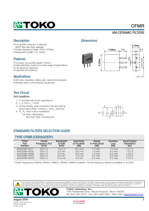
* Center frequencies 450kHz, 455kHz, 459kHz, 460kHz, 468kHz available. Center frequency tolerance available to ±0.5kHz.
The information furnished by TOKO, Inc. is believed to be accurate and reliable. However, TOKO reserves the right to make changes or improvements in the design, specification or manufacture of its products without further notice. TOKO does not assume any liability arising from the application or use of any product or circuit described herein, nor for any infringements of patents or other rights of third parties which may result from the use of its products. No license is granted by implication or otherwise under any patent or patent rights of TOKO, Inc.
© 2005 TOKO America, Inc. All Rights Reserved Printed in USA
CF-314-CFMR R SELECTION GUIDE TYPE CFMR (CERASIZER®)
MBR4045

MBR4035PT THRU MBR4060PTSCHOTTKY RECTIFIERReverse Voltage -35 to 60 Volts Forward Current - 40.0 AmperesFEATURES♦ Plastic package has Underwriters Laboratory Flammability Classifications 94V-0♦ Dual rectifier construction, positive center-tap ♦ Metal silicon rectifier,majority carrier conduction ♦ Low power loss,high efficiency♦ High current capability, low forward voltage drop ♦ High surge capability♦ For use in low voltage, high frequency inverters, free wheeling, and polarity protection applications ♦ Guardring for overvoltage protection ♦ High temperature soldering guaranteed:250°C/10 seconds, 0.17" (4.3mm) from caseMECHANICAL DATACase:JEDEC TO-247AD molded plastic body Terminals:Lead solderable per MIL-STD-750,Method 2026Polarity:As marked Mounting Position:AnyMounting Torque:10 in.- lbs.max.Weight:0.2 ounce, 5.6 gramsMAXIMUM RATINGS AND ELECTRICAL CHARACTERISTICSRatings at 25°C ambient temperature unless otherwise specified.SYMBOLS MBR4035PT MBR4045PT MBR4050PT MBR4060PT UNITSMaximum repetitive peak reverse voltage V RRM 35455060Volts Maximum working peak reverse voltage V RMS 35455060Volts Maximum DC blocking voltageV DC 35455060Volts Maximum average forward rectified current at T C =125°CI (AV)40.0Amps Peak repetitive forward current per leg at T C =120°C (rated V R square wave, 20 KH Z )I FRM 40.0Amps Peak forward surge current, 8.3ms single half sine-wave superimposed on rated load (JEDEC Method)I FSM 400.0AmpsPeak repetitive reverse surge current (NOTE1)I RRM2.01.0AmpsMaximum instantaneous forward voltage per leg at I F =20A, T C =25°C0.700.72(NOTE 2)I F =20A, T C =125°C V F 0.600.62VoltsI F =40A, T C =25°C 0.80_I F =40A, T C =125°C 0.75_Maximum instantaneous reverse current at T C =25°C 1.0rated DC blocking voltage per leg (NOTE 2) T C =125°C I R 100.0mA Typical thermal resistance per leg (NOTE 3)R ΘJC 1.2°C/W Voltage rate of change (rated V R )dv/dt 10,000V/µs Operating junction temperature range T J -65 to +150°C Storage temperature rangeT STG-65 to +175°CNOTES:(1) 2.0µs pulse width, f=1.0 KH Z(2) Pulse test: 300µs pulse width, 1% duty cycle (3) Thermal resistance from junction to case per leg4/981o REF.Dimensions in inches and (millimeters)TO-247AD0.010.11101000.111010050100150010********11010010020030040000.10.20.30.40.50.60.70.80.91.01.11.20.010.1110500.11101001001,0005,000204060801000.0010.010.111050RATINGS AND CHARACTERISTIC CURVES MBR4035PT THRU MBR4060PTT J =150°CFIG. 1 - FORWARD CURRENT DERATING CURVECASE TEMPERATURE, °CA V E R A G E F O R W A R D C U R R E N T ,A M P E R E SFIG. 2 - MAXIMUM NON-REPETITIVE PEAK FORWARDSURGE CURRENT PER LEGNUMBER OF CYCLES AT 60 H ZP E A K F O R W A R D S U R G E C U R R E N T ,A M P E R E SFIG. 3 - TYPICAL REVERSE CHARACTERISTICSPER LEGFIG. 4 - TYPICAL REVERSE CHARACTERISTICSPER LEGI N S T A N T A N E O U S F O R W A R D C U R R E N T , A M P E R E SI N S T A N T A N E O U S R E V E R S E C U R R E N T , M I L L I A M P E R E SINSTANTANEOUS FORWARD VOLTAGE,VOLTSPERCENT OF RATED PEAK REVERSE VOLTAGE, %FIG. 5 - TYPICAL JUNCTION CAPACITANCE PER LEGJ U N C T I O N C A P A C I T A N C E , p FREVERSE VOLTAGE, VOLTST J =T J max.8.3ms SINGLE HALF SINE-WAVE (JEDEC Method)RESISTIVE OR INDUCTIVE LOADT J =75°CT J =25°CT J =25°CPULSE WIDTH=300µs 1%DUTY CYCLET J =125°CFIG . 6 - TYPICAL TRANSIENT THERMAL IMPEDANCEPER LEGt, PULSE DURATION, sec.T R A N S I E N T T H E R M A L I M P E D A N C E , °C /WMBR4035PT - MBR4045PT MBR4050PT & MBR4060PTMBR4035PT - MBR4045PT MBR4050PT & MBR4060PTMBR4035PT - MBR4045PT MBR4050PT & MBR4060PTT J =25°C f=1.0 MHz Vsig=50mVp-p。
MRFE6VP8600HSR5;MRFE6VP8600HR5;MRFE6VP8600HR6;MRFE6VP8600HSR6;中文规格书,Datasheet资料
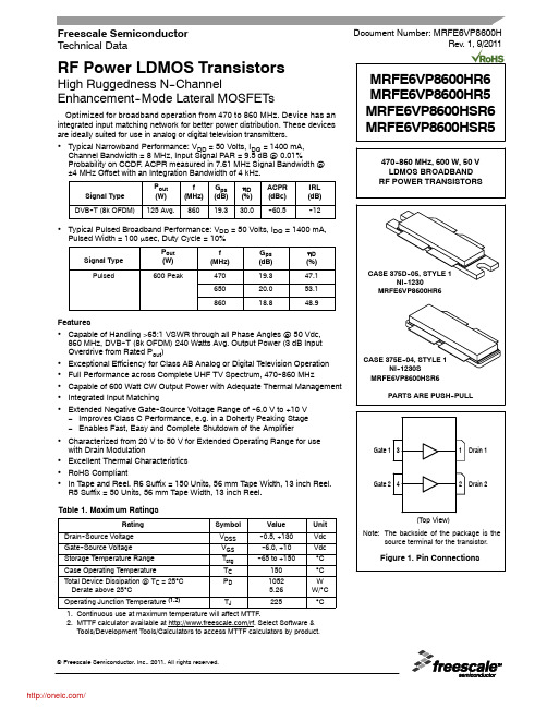
RF POWER TRANSISTORS
CASE 375D--05, STYLE 1 NI--1230
MRFE6VP8600HR6
Features
• Capable of Handling >65:1 VSWR through all Phase Angles @ 50 Vdc, 860 MHz, DVB--T (8k OFDM) 240 Watts Avg. Output Power (3 dB Input Overdrive from Rated Pout)
RF Device Data
Freescale Semiconductor
1
/
Table 2. Thermal Characteristics
Characteristic
Thermal Resistance, Junction to Case Case Temperature 74°C, 125 W CW, 50 V, 1400 mA, 860 MHz
• Typical Narrowband Performance: VDD = 50 Volts, IDQ = 1400 mA, Channel Bandwidth = 8 MHz, Input Signal PAR = 9.5 dB @ 0.01% Probability on CCDF. ACPR measured in 7.61 MHz Signal Bandwidth @ ±4 MHz Offset with an Integration Bandwidth of 4 kHz.
• Excellent Thermal Characteristics • RoHS Compliant • In Tape and Reel. R6 Suffix = 150 Units, 56 mm Tape Width, 13 inch Reel.
mt9045中文资料_数据手册_IC数据表

FS1
FS2
Figure 1 - Functional Block Diagram
Zarlink Semiconductor US Patent No. 5,602,884, UK Patent No. 0772912, France Brevete S.G.D.G. 0772912; Germany DBP No. 69502724.7-08
1
Zarlink Semiconductor Inc. Zarlink, ZL and the Zarlink Semiconductor logo are trademarks of Zarlink Semiconductor Inc.
Copyright 2003, Zarlink Semiconductor Inc. All Rights Reserved.
VSS
1
48 TMS
RST 2
47 TCK
TCLR 3
46 TRST
SECOOR 4
45 TDI
SEC 5
44 TDO
PRI 6
43 PRIOOR
Vdd 7
42 IC
OSCo 8
41 FS1
OSCi 9
40 FS2
Vss 10
39 IC
F16o 11 F0o 12
SSOP
38 37
RSEL MS1
RSP 13 TSP 14
TIE Corrector
Circuit
Virtual Reference
DPLL
Selected
Reference
Reference
Select
MUX
TIE
Corrector
- 1、下载文档前请自行甄别文档内容的完整性,平台不提供额外的编辑、内容补充、找答案等附加服务。
- 2、"仅部分预览"的文档,不可在线预览部分如存在完整性等问题,可反馈申请退款(可完整预览的文档不适用该条件!)。
- 3、如文档侵犯您的权益,请联系客服反馈,我们会尽快为您处理(人工客服工作时间:9:00-18:30)。
RF Power Field Effect TransistorsN-Channel Enhancement-Mode Lateral MOSFETsDesigned for broadband commercial and industrial applications withfrequencies up to 1000 MHz. The high gain and broadband performance ofthese devices make them ideal for large-signal, common-source amplifierapplications in 28 volt base station equipment.•Typical Single-Carrier N-CDMA Performance @ 880 MHz, V DD = 28 Volts,I DQ = 350 mA, P out = 10 Watts Avg., IS-95 CDMA (Pilot, Sync, Paging,Traffic Codes 8 Through 13) Channel Bandwidth = 1.2288 MHz. PAR =9.8 dB @ 0.01% Probability on CCDF.Power Gain — 22.7 dBDrain Efficiency — 32%ACPR @ 750 kHz Offset — -47 dBc @ 30 kHz BandwidthGSM EDGE Application•Typical GSM EDGE Performance: V DD = 28 Volts, I DQ = 350 mA,P out = 16 Watts Avg., Full Frequency Band (921-960 MHz)Power Gain — 20 dBDrain Efficiency — 46%Spectral Regrowth @ 400 kHz Offset = -62 dBcSpectral Regrowth @ 600 kHz Offset = -78 dBcEVM — 1.5% rmsGSM Application•Typical GSM Performance: V DD = 28 Volts, I DQ = 350 mA, P out = 45 Watts,Full Frequency Band (921-960 MHz)Power Gain — 20 dBDrain Efficiency — 68%•Capable of Handling 5:1 VSWR, @ 28 Vdc, 880 MHz, 45 Watts CWOutput Power•Characterized with Series Equivalent Large-Signal Impedance Parameters•Integrated ESD Protection•N Suffix Indicates Lead-Free Terminations•200°C Capable Plastic Package•TO-270-2 in Tape and Reel. R1 Suffix = 500 Units per 24 mm,13 inch Reel.•TO-272-2 in Tape and Reel. R1 Suffix = 500 Units per 44 mm,13 inch Reel.Table 1. Maximum RatingsRating Symbol Value Unit Drain-Source Voltage V DSS -0.5, +68Vdc Gate-Source Voltage V GS -0.5, +12Vdc Total Device Dissipation @ T C = 25°CDerate above 25°CP D1751.0WW/°C Storage Temperature Range T stg-65 to +150°C Operating Junction Temperature T J200°CDocument Number: MRF6S9045Rev. 1, 6/2005 Freescale SemiconductorTechnical DataMRF6S9045NR1MRF6S9045NBR1MRF6S9045MR1MRF6S9045MBR12RF Device DataFreescale SemiconductorMRF6S9045NR1 MRF6S9045NBR1 MRF6S9045MR1 MRF6S9045MBR1Table 2. Thermal CharacteristicsCharacteristicSymbol Value (1,2)Unit Thermal Resistance, Junction to Case Case Temperature 81°C, 45 W CW Case Temperature 79°C, 10 W CWR θJC1.01.1°C/WTable 3. ESD Protection CharacteristicsTest MethodologyClass Human Body Model (per JESD22-A114)1A (Minimum)Machine Model (per EIA/JESD22-A115) A (Minimum)Charge Device Model (per JESD22-C101)IV (Minimum)Table 4. Moisture Sensitivity LevelTest MethodologyRating Package Peak TemperatureUnit Per JESD 22-A113, IPC/JEDEC J-STD-0203260°CTable 5. Electrical Characteristics (T C = 25°C unless otherwise noted)CharacteristicSymbolMinTypMaxUnitOff CharacteristicsZero Gate Voltage Drain Leakage Current (V DS = 68 Vdc, V GS = 0 Vdc)I DSS ——10µAdc Zero Gate Voltage Drain Leakage Current (V DS = 28 Vdc, V GS = 0 Vdc)I DSS ——1µAdc Gate-Source Leakage Current (V GS = 5 Vdc, V DS = 0 Vdc)I GSS——1µAdcOn CharacteristicsGate Threshold Voltage(V DS = 10 Vdc, I D = 200 µA)V GS(th)123Vdc Gate Quiescent Voltage(V DS = 28 Vdc, I D = 350 mAdc)V GS(Q)2 2.94Vdc Drain-Source On-Voltage(V GS = 10 Vdc, I D = 1.0 Adc)V DS(on)—0.220.3Vdc Forward Transconductance (V DS = 10 Vdc, I D = 3 Adc)g fs—4—SDynamic CharacteristicsInput Capacitance(V DS = 28 Vdc ± 30 mV(rms)ac @ 1 MHz, V GS = 0 Vdc)C iss —77—pF Output Capacitance(V DS = 28 Vdc ± 30 mV(rms)ac @ 1 MHz, V GS = 0 Vdc)C oss —27—pF Reverse Transfer Capacitance(V DS = 28 Vdc ± 30 mV(rms)ac @ 1 MHz, V GS = 0 Vdc)C rss—0.78—pFFunctional Tests (In Freescale Test Fixture, 50 ohm system) V DD = 28 Vdc, I DQ = 350 mA, P out = 10 W Avg., f = 880 MHz, Single-Carrier N-CDMA, 1.2288 MHz Channel Bandwidth Carrier. ACPR measured in 30 kHz Channel Bandwidth @ ±750 kHz Offset. PAR = 9.8 dB @ 0.01% Probability on CCDF Power Gain G ps 2122.725dB Drain EfficiencyηD 30.532—%Adjacent Channel Power Ratio ACPR —-47-45dBc Input Return LossMRF6S9045NR1(MR1)MRF6S9045NBR1(MBR1)IRL—-20-20-9-7dB1.MTTF calculator available at /rf. Select Tools/Software/Application Software/Calculators to access the MTTF calculators by product.2.Refer to AN1955, Thermal Measurement Methodology of RF Power Amplifiers. Go to /rf. Select Documentation/Application Notes - AN1955.MRF6S9045NR1 MRF6S9045NBR1 MRF6S9045MR1 MRF6S9045MBR13RF Device DataFreescale SemiconductorTable 5. Electrical Characteristics (T C = 25°C unless otherwise noted) (continued)CharacteristicSymbolMinTypMaxUnitTypical GSM EDGE Performances (In Freescale GSM EDGE Test Fixture Optimized for 921-960 MHz, 50 οhm system) V DD = 28 Vdc, I DQ = 350 mA, P out = 16 W Avg., f = 921-960 MHz, GSM EDGE Signal Power Gain G ps —20—dB Drain Efficiency ηD —46—%Error Vector MagnitudeEVM — 1.5—%Spectral Regrowth at 400 kHz Offset SR1—-62—dBc Spectral Regrowth at 600 kHz OffsetSR2—-78—dBcTypical CW Performances (In Freescale GSM Test Fixture Optimized for 921-960 MHz, 50 οhm system) V DD = 28 Vdc, I DQ = 350 mA, P out = 45 W, f = 921-960 MHz Power Gain G ps —20—dB Drain Efficiency ηD —68—%Input Return LossIRL —-12—dB P out @ 1 dB Compression Point (f = 940 MHz)P1dB—52—W4RF Device DataFreescale SemiconductorMRF6S9045NR1 MRF6S9045NBR1 MRF6S9045MR1 MRF6S9045MBR1Figure 1. MRF6S9045NR1(MR1)/NBR1(MBR1) Test Circuit SchematicZ100.360″ x 0.270″ Microstrip Z110.063″ x 0.270″ Microstrip Z120.360″ x 0.065″ Microstrip Z130.095″ x 0.065″ Microstrip Z140.800″ x 0.065″ Microstrip Z150.260″ x 0.065″ Microstrip Z160.325″ x 0.065″ MicrostripPCBTaconic RF-35 0.030″, εr = 3.5Z10.215″ x 0.065″ MicrostripZ20.221″ x 0.065″ Microstrip Z30.500″ x 0.100″ Microstrip Z40.460″ x 0.270″ Microstrip Z50.040″ x 0.270″ MicrostripZ60.280″ x 0.270″ x 0.530″Taper Z70.087″ x 0.525″ Microstrip Z80.435″ x 0.525″ Microstrip Z90.057″ x 0.525″ MicrostripTable 6. MRF6S9045NR1(MR1)/NBR1(MBR1) Test Circuit Component Designations and ValuesPartDescriptionPart NumberManufacturer B1Ferrite Bead 2743019447Fair Rite B2Ferrite Bead2743021447Fair Rite C1, C7, C10, C1447 pF Chip Capacitors100B470JP500X ATC C2, C4, C120.8-8.0 pF Variable Capacitors, Gigatrim 27291SL Johanson C315 pF Chip Capacitor 100B150JP500X ATC C5, C612 pF Chip Capacitors 100B120JP500X ATC C8, C913 pF Chip Capacitors 100B130JP500X ATC C117.5 pF Chip Capacitor100B7R5JP500X ATC C130.6-4.5 pF Variable Capacitor, Gigatrim 27271SLJohanson C15, C16, C1710 µF, 35 V Tantalum Capacitors T491D106K035AS Kemet C18220 µF, 50 V Electrolytic Capacitor 678D227M025CG3D Vishay L1, L212.5 nH Inductor A04T-5Coilcraft R1 1 k Ω Chip Resistor CRCW12061001F100Vishay Dale R2560 k Ω Chip Resistor CRCW12065603F100Vishay Dale R312 Ω Chip ResistorCRC120612R0F100Vishay DaleMRF6S9045NR1 MRF6S9045NBR1 MRF6S9045MR1 MRF6S9045MBR15RF Device DataFreescale SemiconductorFigure 2. MRF6S9045NR1(MR1)/NBR1(MBR1) Test Circuit Component Layout6RF Device DataFreescale SemiconductorMRF6S9045NR1 MRF6S9045NBR1 MRF6S9045MR1 MRF6S9045MBR1TYPICAL CHARACTERISTICSFigure 5. Two-Tone Power Gain versusOutput Power 1001924P out , OUTPUT POWER (WATTS) PEP222010G p s , P O W E R G A I N (d B )23211300Figure 6. Third Order Intermodulation Distortionversus Output Power1P out , OUTPUT POWER (WATTS) PEP101000.5MRF6S9045NR1 MRF6S9045NBR1 MRF6S9045MR1 MRF6S9045MBR17RF Device DataFreescale SemiconductorTYPICAL CHARACTERISTICSFigure 7. Intermodulation Distortion Productsversus Output Power10−80−10P out , OUTPUT POWER (WATTS) PEP−20−30−401100I M D , I N T E R M O D U L A T I O N D I S T O R T I O N (d B c )−50−60−70Figure 8. Intermodulation Distortion Productsversus Tone Spacing10−7000.05TWO−TONE SPACING (MHz)−10−20−30−40−50−601100I M D , I N T E R M O D U L A T I O N D I S T O R T I O N (d B c )0.1Figure 9. Pulse CW Output Power versusInput Power3354P in , INPUT POWER (dBm)525048442426252827312953495147303223P o u t , O U T P U T P O W E R (d B m )4645Figure 10. Single-Carrier N-CDMA ACPR, ALT1, PowerGain and Drain Efficiency versus Output Power0−85P out , OUTPUT POWER (WATTS) AVG.60−2550−3540−4530−5510−75110−6520ηD , D R A I N E F F I C I E N C Y (%), G p s , P O W E R G A I N (d B )A L T 1, C H A N N E L P O W E R (dB c )A C P R , A D J A C E N T C H A N N E L P O W E R R A T I O (dB c )508RF Device DataFreescale SemiconductorMRF6S9045NR1 MRF6S9045NBR1 MRF6S9045MR1 MRF6S9045MBR1TYPICAL CHARACTERISTICS2423222018ηD , D R A I N E F F I C I E N C Y (%)G p s , P O W E R G A I N (d B )G p s , P O W E R G A I N (d B )2119171621010T J , JUNCTION TEMPERATURE (°C)This above graph displays calculated MTTF in hours x ampere 2drain current. Life tests at elevated temperatures have correlated to better than ±10% of the theoretical prediction for metal failure. Divide MTTF factor by I D 2 for MTTF in a particular application.101010M T T F F A C T O R (H O U R S X A M P S 2)90110130150170190Figure 13. MTTF Factor versus Junction Temperature100120140160180200MRF6S9045NR1 MRF6S9045NBR1 MRF6S9045MR1 MRF6S9045MBR19RF Device DataFreescale SemiconductorN-CDMA TEST SIGNAL100.00011000PEAK −TO−AVERAGE (dB)Figure 14. Single-Carrier CCDF N-CDMA1010.10.010.0012468P R O B A B I L I T Y (%)−60−110−10(d B )−20−30−40−50−70−80−90−1002.90.7 2.21.50−0.7−1.5−2.2−2.9−3.6 3.6f, FREQUENCY (MHz)Figure 15. Single-Carrier N-CDMA Spectrum10RF Device DataFreescale SemiconductorMRF6S9045NR1 MRF6S9045NBR1 MRF6S9045MR1 MRF6S9045MBR1Figure 16. Series Equivalent Source and Load Impedancef MHz Z sourceΩZ load Ω850865880 3.05 + j1.273.31 + j1.333.16 + j1.330.42 + j0.300.42 + j0.440.45 + j0.60V DD = 28 Vdc, I DQ = 350 mA, P out = 10 W Avg.8959103.35 + j1.053.43 + j1.200.48 + j0.740.50 + j0.85Z source =Test circuit impedance as measured fromgate to ground.Zload=Test circuit impedance as measured from drain to ground.ZsourceZloadOutput Matching NetworkZ o = 5 ΩZ sourcef = 850 MHzf = 910 MHzZ loadf = 910 MHzf = 850 MHzMRF6S9045NR1 MRF6S9045NBR1 MRF6S9045MR1 MRF6S9045MBR111RF Device DataFreescale SemiconductorNOTES12RF Device Data Freescale SemiconductorMRF6S9045NR1 MRF6S9045NBR1 MRF6S9045MR1 MRF6S9045MBR1NOTESMRF6S9045NR1 MRF6S9045NBR1 MRF6S9045MR1 MRF6S9045MBR113RF Device DataFreescale SemiconductorNOTES14RF Device DataFreescale SemiconductorMRF6S9045NR1 MRF6S9045NBR1 MRF6S9045MR1 MRF6S9045MBR1PACKAGE DIMENSIONSTO-270-2PLASTICCASE 1265-08ISSUE HMRF6S9045NR1(MR1)MRF6S9045NR1 MRF6S9045NBR1 MRF6S9045MR1 MRF6S9045MBR115RF Device DataFreescale SemiconductorCASE 1337-03ISSUE C AREA OF THE HEAT SLUG.DIM A MIN MAX MIN MAX MILLIMETERS .100.104 2.54 2.64INCHES A1.039.0430.99 1.09A2.040.042 1.02 1.07D .928.93223.5723.67D1E .438.44211.1211.23E1.248.252 6.30 6.40F b1.193c1.007.011.18r1.063.0681.60aaa1.810 BSC .00420.57 BSC .10STYLE 1:PIN 1.DRAIN2.GATE3.SOURCE.025 BSC .281.73.199 4.900.64 BSC5.05E2.241.2456.12 6.22TO-272-2PLASTICMRF6S9045NBR1(MBR1)Information in this document is provided solely to enable system and softwareimplementers to use Freescale Semiconductor products. There are no express orimplied copyright licenses granted hereunder to design or fabricate any integratedcircuits or integrated circuits based on the information in this document.Freescale Semiconductor reserves the right to make changes without further notice toany products herein. Freescale Semiconductor makes no warranty, representation orguarantee regarding the suitability of its products for any particular purpose, nor doesFreescale Semiconductor assume any liability arising out of the application or use ofany product or circuit, and specifically disclaims any and all liability, including withoutlimitation consequential or incidental damages. “Typical” parameters that may beprovided in Freescale Semiconductor data sheets and/or specifications can and dovary in different applications and actual performance may vary over time. All operatingparameters, including “Typicals”, must be validated for each customer application bycustomer’s technical experts. Freescale Semiconductor does not convey any licenseunder its patent rights nor the rights of others. Freescale Semiconductor products arenot designed, intended, or authorized for use as components in systems intended forsurgical implant into the body, or other applications intended to support or sustain life,or for any other application in which the failure of the Freescale Semiconductor productcould create a situation where personal injury or death may occur. Should Buyerpurchase or use Freescale Semiconductor products for any such unintended orunauthorized application, Buyer shall indemnify and hold Freescale Semiconductorand its officers, employees, subsidiaries, affiliates, and distributors harmless against allclaims, costs, damages, and expenses, and reasonable attorney fees arising out of,directly or indirectly, any claim of personal injury or death associated with suchunintended or unauthorized use, even if such claim alleges that FreescaleSemiconductor was negligent regarding the design or manufacture of the part.Freescale t and the Freescale logo are trademarks of Freescale Semiconductor, Inc.All other product or service names are the property of their respective owners.Freescale Semiconductor, Inc. 2005. All rights reserved.How to Reach Us:Home Page:E-mail:support@USA/Europe or Locations Not Listed:Freescale SemiconductorTechnical Information Center, CH3701300 N. Alma School RoadChandler, Arizona 85224+1-800-521-6274 or +1-480-768-2130support@Europe, Middle East, and Africa:Freescale Halbleiter Deutschland GmbHTechnical Information CenterSchatzbogen 781829 Muenchen, Germany+44 1296 380 456 (English)+46 8 52200080 (English)+49 89 92103 559 (German)+33 1 69 35 48 48 (French)support@Japan:Freescale Semiconductor Japan Ltd.HeadquartersARCO Tower 15F1-8-1, Shimo-Meguro, Meguro-ku,Tokyo 153-0064Japan0120 191014 or +81 3 5437 9125support.japan@Asia/Pacific:Freescale Semiconductor Hong Kong Ltd.Technical Information Center2 Dai King StreetTai Po Industrial EstateTai Po, N.T., Hong Kong+800 2666 8080@For Literature Requests Only:Freescale Semiconductor Literature Distribution CenterP.O. Box 5405Denver, Colorado 802171-800-441-2447 or 303-675-2140Fax: 303-675-2150LDCForFreescaleSemiconductor@。