CAT5113SI-00MSOP中文资料
数冠SGPT5903C 5.0mm NPN 达林顿光敏三极管 用户手册说明书
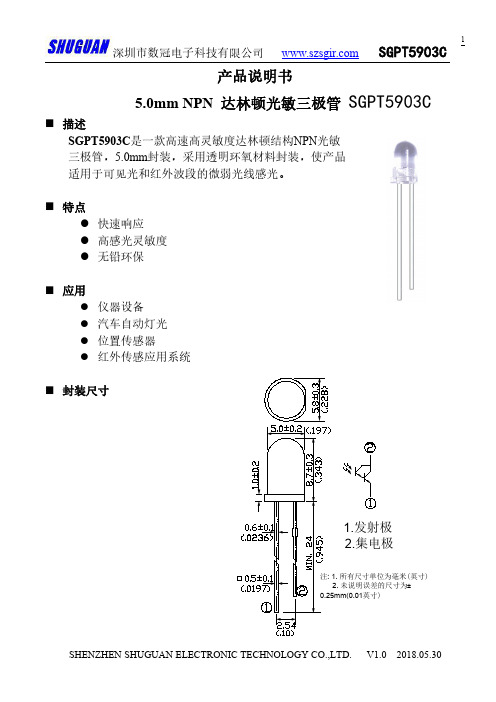
1.发射极2.集电极注: 1. 所有尺寸单位为毫米(英寸) 2. 未说明误差的尺寸为±0.25mm(0.01英寸)产品说明书5.0mm NPN 达林顿光敏三极管SGPT5903C⏹描述SGPT5903C 是一款高速高灵敏度达林顿结构NPN 光敏三极管,5.0mm 封装,采用透明环氧材料封装,使产品适用于可见光和红外波段的微弱光线感光。
⏹特点●快速响应●高感光灵敏度●无铅环保⏹应用●仪器设备●汽车自动灯光●位置传感器●红外传感应用系统⏹封装尺寸⏹极限参数(Ta=25℃)参数名称符号参考值单位集电极-发射极电压V CEO60V发射极-集电极电压V ECO7.0V集电极电流Ic50mA焊接温度*1Tsol260℃工作温度Topr-20~+85℃存储温度Tstg-40~+85℃说明:*1:焊接时间≦5seconds.⏹光电参数(Ta=25℃)参数名称符号最小典型最大单位测试条件频谱范围λ0.5600--1000nm感光峰值波长λP--800--nm集电极–发射极击穿电压BV CEO60----V Ic=100μA,Ee=0mW/cm2发射极-集电极击穿电压BV ECO7.0----V Ic=100μA,Ee=0mW/cm2集电极暗电流I CEO----1000nA V CE=10V,Ee=0mW/cm2集电极-发射极饱和电压V CE(S)--- 1.0V Ic=15mA,Ib=100uA基极-发射极饱和电压V BE(S)--- 1.45V Ic=15mA,Ib=100uA集电极电流I C(on) 2.5 2.8--mA Ev=100Lx,V CE=5V 直流电流放大倍数H FE30000--90000V CE=5V,IC=10mA 上升/下降时间t r/t f--60/60μS V CE=5V,I C=1mAR L=100ΩAmbient Temperature Ta(°C)C o l l e c t o r P o w e rD i s s i p a t i o n (m W )50125020406080100-20-4075100251008060200500Wavelength(nm)R e l a t i v e S p e c t r a l S e n s i t i v i t y (%)Ta=25°4060070080090010001100300Ambient Temperature Ta(°C)R e l a t i v e C o l l e c t o r C u r r e n t (%)40608060100160Vce=5V204080120140Ee=1mW/cm 21020507010Luminance E (Lx )C o l l e c t o r C u r r e n t I c (m A )100100011010101010210Vce=5VT =25 Ca ° 特性曲线图图.1集电极耗散功率与环境温度图.2相对频谱灵敏度图.3相对集电极电流与环境温度图.4集电极电流与辐照度25Ambient Temperature (°C)C o l l e c t o rD a r k C u r r e n t I CE O (n A )50751000Vce=10V 105101010100Collector-Emitter Voltage V CE (V)C o l l e c t o r C u r r e n t I c (m A )12341.02.03.04.05.06.07.0E=10 LxE=50 Lx E=15 LxE=100 LxE=150 Lx 图.5集电极暗电流与环境温度图.6集电极电流与集射电压注意事项:1.我公司保留更改产品材料和以上说明书的权利,更改以上产品说明书恕不另行通知。
Oki Data C310dn C330dn C530dn 多功能打印机说明书

C310dn、C330dn、C530dn维修手册[版本 1]相关图纸图纸编号名称44346007TL C310dn、C330dn、C530dn维修拆卸44346007TR C310dn、C330dn、C530dn RSPL材料表用于认证机构修订日期 DCO号目录设计审批————————————————审批:Naoki Sunaga ……………………………… 设计:Naoki Sunaga………………………………………..名称:C310dn、C330dn、C530dn维修手册审核:…………………………..…. ………………………………………...日期:2010年6月18日Oki公司图纸号:44346001TH 1/17344346001 TH Rev.1文档修订历史版本号日期修正项目负责人序号页码更改说明1 2010-06-18出版S.Ogashiwa 版本号日期修正项目负责人序号页码更改说明44346001 TH Rev.12/序言本手册对维修C310dn、C330dn、C530dn打印机方法进行了介绍。
本手册专为维修人员编制。
想要了解更多有关C310dn、C330dn、C530dn 打印机的使用信息,请参考相关用户手册。
在本手册中这类打印机的名称可能表示为:C310dn-C310C330dn-C330C530dn-C530注!本手册内容如进行修改,恕不另行通知。
z虽然在编写本手册时,为确保其准确性进行了不懈努力,但本手册仍可能会出现错误。
对于由用户根据此手册自行维修/调整/更换打印机而造成的损害,Oki公司不承担任何责任。
z用于C310dn、C330dn、C530dn打印机的零部件非常精细,如果处理不当,此类部件可能损坏。
Oki公司强烈建议由注册维修人员对此类打印机进行维修。
z请在去除静电后再进行操作。
44346001 TH Rev.13/1. 配置1.1 系统配置 (5)1.2 打印机配置 (8)1.3可选部件 (9)1.4说明 (10)44346001 TH Rev.11.1 系统配置图1-1-1和1-1-2表示C310dn、C330dn、C530dn打印机系统配置。
CAT5113P-00MSOP中文资料

CAT5111100-Tap Digitally Programmable Potentiometer (DPP™)with Buffered Wiper FEATURESs 100-position linear taper potentiometer s Non-volatile NVRAM wiper storage;buffered wipers Low power CMOS technology s Single supply operation: 2.5V-6.0V s Increment up/down serial interface s Resistance values: 10k Ω, 50k Ω and 100k Ωs Available in PDIP, SOIC, TSSOP and MSOP packagesAPPLICATIONSs Automated product calibration s Remote control adjustments s Offset, gain and zero control s Tamper-proof calibrationss Contrast, brightness and volume controls s Motor controls and feedback systems s Programmable analog functionssystem values without effecting the stored setting. Wiper-control of the CAT5111 is accomplished with three input control pins, CS , U/D ,and INC . The INC input increments the wiper in the direction which is determined by the logic state of the U/D input. The CS input is used to select the device and also store the wiper position prior to power down.The digitally programmable potentiometer can be used as a buffered voltage divider. For applications where the potentiometer is used as a 2-terminal variable resistor, please refer to the CAT5113. The buffered wiper of the CAT5111 is not compatible with that application. DPPs bring variability and programmability to a broad range of applications and are used primarily to control, regulate or adjust a characteristic or parameter of an analog circuit.FUNCTIONAL DIAGRAMDESCRIPTIONThe CAT5111 is a single digitally programmable potentiometer (DPP™) designed as a electronic replacement for mechanical potentiometers and trim pots. Ideal for automated adjustments on high volume production lines, they are also well suited for applications where equipment requiring periodic adjustment is either difficult to access or located in a hazardous or remote environment.The CAT5111 contains a 100-tap series resistor array connected between two terminals R H and R L . An up/down counter and decoder that are controlled by three input pins, determines which tap is connected to the wiper, R WB . The CAT5111 wiper is buffered by an op amp that operates rail to rail. The wiper setting, stored in non-volatile NVRAM memory, is not lost when the device is powered down and is automatically recalled when power is returned. The wiper can be adjusted to test new Electronic PotentiometerImplementationWBCSINC U /DV WBHLGND© 2004 by Catalyst Semiconductor, Inc.Characteristics subject to change without noticeDoc. No. 2008, Rev. O1HAL O G E N F R E ETML EA D F R E ECAT51112Doc. No. 2008, Rev. Oof the CAT5111 and is active low. When in a high state, activity on the INC and U/D inputs will not affect or change the position of the wiper.DEVICE OPERATIONThe CAT5111 operates like a digitally controlled potentiometer with R H and R L equivalent to the high and low terminals and R WB equivalent to the mechanical potentiometer's wiper. There are 100 available tap positions including the resistor end points, R H and R L .There are 99 resistor elements connected in series between the R H and R L terminals. The wiper terminal is connected to one of the 100 taps and controlled by three inputs, INC , U/D and CS . These inputs control a seven-bit up/down counter whose output is decoded to select the wiper position. The selected wiper position can be stored in nonvolatile memory using the INC and CS inputs.With CS set LOW the CAT5111 is selected and will respond to the U/D and INC inputs. HIGH to LOW transitions on INC wil increment or decrement the wiper (depending on the state of the U/D input and seven-bit counter). The wiper, when at either fixed terminal, acts like its mechanical equivalent and does not move beyond the last position. The value of the counter is stored in nonvolatile memory whenever CS transitions HIGH while the INC input is also HIGH. When the CAT5111 is powered-down, the last stored wiper counter position is maintained in the nonvolatile memory.When power is restored, the contents of the memory are recalled and the counter is set to the value stored.With INC set low, the CAT5111 may be de-selected and powered down without storing the current wiper position in nonvolatile memory. This allows the system to always power up to a preset value stored in nonvolatile memory.PIN DESCRIPTIONSINC : Increment Control InputThe INC input (on the falling edge) moves the wiper in the up or down direction determined by the condition of the U/D input.U/D : Up/Down Control InputThe U/D input controls the direction of the wiper movement. When in a high state and CS is low, any high-to-low transition on INC will cause the wiper to move one increment toward the R H terminal. When in a low state and CS is low, any high-to-low transition on INC will cause the wiper to move one increment towards the R L terminal.R H: High End Potentiometer TerminalR H is the high end terminal of the potentiometer. It is not required that this terminal be connected to a potential greater than the R L terminal. Voltage applied to the R H terminal cannot exceed the supply voltage, V CC or go below ground, GND.R WB : Wiper Potentiometer Terminal (Buffered)R WB is the buffered wiper terminal of the potentiometer. Its position on the resistor array is controlled by the control inputs, INC , U/D and CS .R L : Low End Potentiometer TerminalR L is the low end terminal of the potentiometer. It is not required that this terminal be connected to a potential less than the R H terminal. Voltage applied to the R L terminal cannot exceed the supply voltage, V CC or go below ground, GND. R L and R H are electrically interchangeable.CS : Chip SelectThe chip select input is used to activate the control inputPIN FUNCTIONSPin Name FunctionINC Increment Control U/D Up/Down ControlR H Potentiometer High Terminal GND GroundR WB Buffered Wiper Terminal R L Potentiometer Low Terminal CS Chip Select V CCSupply VoltagePIN CONFIGURATIONPDIP Package (P, L)TSSOP Package (U, Y)MSOP Package (R, Z)INC V CC CS R L R WB U /DR HGND 12348765CS INC V CC R L R WBU /D R H GND12348765V CC R L R WBGNDR H INC U/D CS 12348765CS INC V CC R L R WBU /D R H GND12348765SOIC Package (S, V)CAT51113Doc. No. 2008, Rev. OOPERATING MODESABSOLUTE MAXIMUM RATINGS Supply VoltageV CC to GND –0.5V to +7V InputsCS to GND –0.5V to V CC +0.5V INC to GND –0.5V to V CC +0.5V U/D to GND –0.5V to V CC +0.5V R H to GND –0.5V to V CC +0.5V R L to GND –0.5V to V CC +0.5V R WB to GND–0.5V to V CC +0.5VOperating Ambient TemperatureCommercial (‘C ’ or Blank suffix)0°C to +70°C Industrial (‘I ’ suffix)– 40°C to +85°C Junction Temperature +150°C Storage Temperature –65°C to +150°C Lead Soldering (10 sec max)+300°C* Stresses above those listed under Absolute Maximum Ratings may cause permanent damage to the device. Absolute Maximum Ratings are limited values applied individually while other parameters are within specified operating conditions, and functional operation at any of these conditions is NOT implied. Device performance and reliability may be impaired by exposure to absolute rating conditions for extended periods of time.NOTES:(1)This parameter is tested initially and after a design or process change that affects the parameter.(2)Latch-up protection is provided for stresses up to 100mA on address and data pins from –1V to V CC + 1V (3)I W =source or sink(4)These parameters are periodically sampled and are not 100% tested.C C WB Power SupplySymbol Parameter Conditions MinTypMaxUnitsV CC Operating Voltage Range2.5— 6.0V I CC1Supply Current (Increment) V CC = 6V, f = 1MHz, I W =0——200µA V CC = 6V, f = 250kHz, I W =0——100I CC2Supply Current (Write) Programming, V CC = 6V——1mA V CC = 3V ——500µA ISB 1 (2)Supply Current (Standby)CS=V CC -0.3V—75150µAU/D, INC=V CC -0.3V or GNDDC Electrical Characteristics: V CC = +2.5V to +6.0V unless otherwise specifiedINC CS U/D Operation High to Low Low High Wiper toward R H High to Low Low Low Wiper toward R L High Low to High X Store Wiper Position Low Low to High X No Store, Return to Standby XHighXStandbyRELIABILITY CHARACTERISTICS SymbolParameterTest MethodMinTyp Max UnitsV ZAP (1)ESD Susceptibility MIL-STD-883, Test Method 30152000Volts I LTH (1)(2)Latch-UpJEDEC Standard 17100mA T DR Data Retention MIL-STD-883, Test Method 1008100Years N ENDEnduranceMIL-STD-883, Test Method 10031,000,000StoresCAT51114Doc. No. 2008, Rev. OSymbol ParameterConditions Min Typ Max Units R POTPotentiometer Resistance-10 Device 10-50 Device 50 k Ω-00 Device100Pot Resistance Tolerance±20% V RH Voltage on R H pin 0 V CC VV RL Voltage on R L pin 0V CCVResolution1% INL Integral Linearity Error I W ≤ 2µA 0.5 1 LSB DNL Differential Linearity Error I W ≤ 2µA0.250.5 LSB R OUT Buffer Output Resistance .05V CC ≤ V WB ≤ .95V CC , V CC =5V 1 Ω I OUT Buffer Output Current .05V CC ≤ V WB ≤ .95V CC , V CC =5V3mA TC RPOT TC of Pot Resistance 300ppm/o C TC RATIO Ratiometric TC TBD ppm/o C R ISOIsolation Resistance TBDΩ C RH /C RL /C RWPotentiometer Capacitances 8/8/25pF fc Frequency Response Passive Attenuator, 10k Ω 1.7MHzV WB(SWING)Output Voltage RangeI OUT ≤100µA, V CC =5V0.01V CC.99V CCPotentiometer ParametersCAT51115Doc. No. 2008, Rev. OV CC Range 2.5V ≤ V CC ≤ 6V Input Pulse Levels 0.2V CC to 0.7V CC Input Rise and Fall Times 10ns Input Reference Levels0.5V CCAC CONDITIONS OF TEST A. C. TIMING(1)Typical values are for T A =25˚C and nominal supply voltage.(2)This parameter is periodically sampled and not 100% tested.(3)MI in the A.C. Timing diagram refers to the minimum incremental change in the W output due to a change in the wiper position.CSU R WBSymbolParameterMinTyp (1)MaxUnitst CI CS to INC Setup 100——ns t DI U/D to INC Setup 50——ns t ID U/D to INC Hold 100——ns t IL INC LOW Period 250——ns t IH INC HIGH Period250——ns t IC INC Inactive to CS Inactive1——µs t CPH CS Deselect Time (NO STORE)100——ns t CPH CS Deselect Time (STORE)10——ms t IW INC to V OUT Change —15µs t CYC INC Cycle Time1——µs t R, t F (2)INC Input Rise and Fall Time ——500µs t PU (2)Power-up to Wiper Stable ——1msec t WRStore Cycle—510msAC OPERATING CHARACTERISTICS:V CC = +2.5V to +6.0V, V H = V CC , V L = 0V , unless otherwise specifiedCAT51116Doc. No. 2008, Rev. OORDERING INFORMATIONNotes:(1) The device used in the above example is a CAT5111 SI-10TE13 (SOIC, 10K Ohms, Industrial Temperature, Tape & Reel)CAT5111Catalyst Semiconductor, Inc.Corporate Headquarters 1250 Borregas AvenueSunnyvale, CA 94089Phone: 408.542.1000Fax: 408.542.1200Copyrights, Trademarks and PatentsTrademarks and registered trademarks of Catalyst Semiconductor include each of the following:DPP ™AE 2 ™Catalyst Semiconductor has been issued U.S. and foreign patents and has patent applications pending that protect its products. For a complete list of patents issued to Catalyst Semiconductor contact the Company’s corporate office at 408.542.1000.CATALYST SEMICONDUCTOR MAKES NO WARRANTY, REPRESENTATION OR GUARANTEE, EXPRESS OR IMPLIED, REGARDING THE SUITABILITY OF ITS PRODUCTS FOR ANY PARTICULAR PURPOSE, NOR THAT THE USE OF ITS PRODUCTS WILL NOT INFRINGE ITS INTELLECTUAL PROPERTY RIGHTS OR THE RIGHTS OF THIRD PARTIES WITH RESPECT TO ANY PARTICULAR USE OR APPLICATION AND SPECIFICALLY DISCLAIMS ANY AND ALL LIABILITY ARISING OUT OF ANY SUCH USE OR APPLICATION, INCLUDING BUT NOT LIMITED TO, CONSEQUENTIAL OR INCIDENTAL DAMAGES.Catalyst Semiconductor products are not designed, intended, or authorized for use as components in systems intended for surgical implant into the body, or other applications intended to support or sustain life, or for any other application in which the failure of the Catalyst Semiconductor product could create a situation where personal injury or death may occur.Catalyst Semiconductor reserves the right to make changes to or discontinue any product or service described herein without notice. Products with data sheets labeled "Advance Information" or "Preliminary" and other products described herein may not be in production or offered for sale.Catalyst Semiconductor advises customers to obtain the current version of the relevant product information before placing orders. Circuit diagrams illustrate typical semiconductor applications and may not be complete.Publication #:2002Revison:OIssue date:4/12/04REVISION HISTORY。
毛斯(Moxa)UC-8200系列双核ARM Cortex-A7 1GHz IIoT网关产品说明书
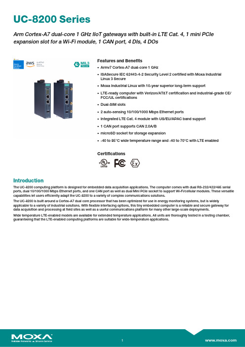
UC-8200SeriesArm Cortex-A7dual-core1GHz IIoT gateways with built-in LTE Cat.4,1mini PCIe expansion slot for a Wi-Fi module,1CAN port,4DIs,4DOsFeatures and Benefits•Armv7Cortex-A7dual-core1GHz•ISASecure IEC62443-4-2Security Level2certified with Moxa IndustrialLinux3Secure•Moxa Industrial Linux with10-year superior long-term support•LTE-ready computer with Verizon/AT&T certification and industrial-grade CE/FCC/UL certifications•Dual-SIM slots•2auto-sensing10/100/1000Mbps Ethernet ports•Integrated LTE Cat.4module with US/EU/APAC band support•1CAN port supports CAN2.0A/B•microSD socket for storage expansion•-40to85°C wide temperature range and-40to70°C with LTE enabledCertificationsIntroductionThe UC-8200computing platform is designed for embedded data acquisition applications.The computer comes with dual RS-232/422/485serial ports,dual10/100/1000Mbps Ethernet ports,and one CAN port as well as dual Mini PCIe socket to support Wi-Fi/cellular modules.These versatile capabilities let users efficiently adapt the UC-8200to a variety of complex communications solutions.The UC-8200is built around a Cortex-A7dual core processor that has been optimized for use in energy monitoring systems,but is widely applicable to a variety of industrial solutions.With flexible interfacing options,this tiny embedded computer is a reliable and secure gateway for data acquisition and processing at field sites as well as a useful communications platform for many other large-scale deployments.Wide temperature LTE-enabled models are available for extended temperature applications.All units are thoroughly tested in a testing chamber, guaranteeing that the LTE-enabled computing platforms are suitable for wide-temperature applications.AppearanceUC-8210UC-8220SpecificationsComputerCPU Armv7Cortex-A7dual-core1GHzDRAM2GB DDR3LSupported OS Moxa Industrial Linux1(Debian9,kernel4.4),2027EOLMoxa Industrial Linux31(Debian11,kernel5.10),2031EOLSee /MILStorage Pre-installed8GB eMMCExpansion Slots MicroSD(SD3.0)socket x13OS is selectable via Moxa Computer Configuration System(CCS)for CTO models.For the model names,see the Ordering Information section of thedatasheet PDF file.Computer InterfaceEthernet Ports Auto-sensing10/100/1000Mbps ports(RJ45connector)x2 Serial Ports RS-232/422/485ports x2,software selectable(DB9male) CAN Ports CAN2.0A/B x1(DB9male)Digital Input DIs x4Digital Output DOs x4USB2.0USB2.0hosts x1,type-A connectorsWi-Fi Antenna Connector UC-8220Models:RP-SMA x2Cellular Antenna Connector UC-8220Models:SMA x2GPS Antenna Connector UC-8220Models:SMA x1Expansion Slots UC-8220-T-LX:mPCIe slot x2UC-8220-T-LX US/EU/AP Models:mPCIe slot x1SIM Format UC-8220Models:NanoNumber of SIMs UC-8220Models:2Buttons Programmable buttonTPM TPM v2.0Ethernet InterfaceMagnetic Isolation Protection 1.5kV(built-in)Security FunctionsHardware-based Security TPM2.0Hardware Root of Trust Secure BootIntrusion Detection Host-based Intrusion DetectionSecurity Tools Security Diagnostic ToolSecurity Event AuditingSecure UpdateDisk Protection LUKS Disk EncryptionRecovery One-step recovery to the last known secure stateDual-system design with automatic failbackReliability Network Keep AliveNetwork Failover and FailbackSerial InterfaceBaudrate300bps to921.6kbpsData Bits7,8Stop Bits1,2Parity None,Even,Odd,Space,MarkFlow Control RTS/CTS,XON/XOFFADDC(automatic data direction control)for RS-485RTS Toggle(RS-232only)Console Port1x4-pin header to DB9console portRS-232TxD,RxD,RTS,CTS,DTR,DSR,DCD,GNDRS-422Tx+,Tx-,Rx+,Rx-,GNDRS-485-2w Data+,Data-,GNDCAN InterfaceNo.of Ports1Connector DB9maleBaudrate10to1000kbpsIndustrial Protocols CAN2.0ACAN2.0BIsolation2kV(built-in)Signals CAN_H,CAN_L,CAN_GND,CAN_SHLD,CAN_V+,GNDDigital InputsConnector Screw-fastened Euroblock terminalDry Contact Off:openOn:short to GNDIsolation3K VDCSensor Type Wet contact(NPN)Dry contactWet Contact(DI to COM)On:10to30VDCOff:0to3VDCDigital OutputsConnector Screw-fastened Euroblock terminalCurrent Rating200mA per channelI/O Type SinkVoltage24VDC nominal,open collector to30VDCCellular InterfaceCellular Standards LTE Cat.4Band Options US Models:LTE Band2(1900MHz)/LTE Band4(1700MHz)/LTE Band5(850MHz)/LTE Band13(700MHz)/LTE Band17(700MHz)UMTS/HSPA850MHz/1900MHzCarrier Approval:Verizon,AT&TEU Models:LTE Band1(2100MHz)/LTE Band3(1800MHz)/LTE Band5(850MHz)/LTE Band7(2600MHz)/LTE Band8(900MHz)/LTE Band20(800MHz)UMTS/HSPA850MHz/900MHz/1900MHz/2100MHzAP Models:LTE Band1(2100MHz)/LTE Band3(1800MHz)/LTE Band5(850MHz)/LTE Band7(2600MHz)/LTE Band8(900MHz)/LTE Band28(700MHz)UMTS/HSPA850MHz/900MHz/1900MHz/2100MHzReceiver Types GPS/GLONASS/GalileoState-of-the-art GNSS solutionAccuracy Position:2.0m@CEP50Acquisition Hot starts:1.1secCold starts:29.94secSensitivity Cold starts:-145dBmTracking:-160dBmTime Pulse0.25Hz to10MHzLED IndicatorsSystem Power x2Programmable x1SIM card indicator x1Wireless Signal Strength Cellular/Wi-Fi x6Power ParametersNo.of Power Inputs Redundant dual inputsInput Voltage12to48VDCPower Consumption10WInput Current0.8A@12VDCReliabilityAlert Tools External RTC(real-time clock)Automatic Reboot Trigger External WDT(watchdog timer)Physical CharacteristicsDimensions UC-8220Models:141.5x120x39mm(5.7x4.72x1.54in)UC-8210Models:141.5x120x27mm(5.7x4.72x1.06in)141.5x120x27mm(5.7x4.72x1.06in)Weight UC-8210Models:560g(1.23lb)UC-8220Models:750g(1.65lb)Housing SECCMetalIP Rating IP30Installation DIN-rail mountingWall mounting(with optional kit)Environmental LimitsOperating Temperature-40to70°C(-40to158°F)Storage Temperature(package included)-40to85°C(-40to185°F)Ambient Relative Humidity5to95%(non-condensing)Shock IEC60068-2-27Vibration2Grms@IEC60068-2-64,random wave,5-500Hz,1hr per axis(without USB devicesattached)Standards and CertificationsEMC EN55032/35EN61000-6-2/-6-4EMI CISPR32,FCC Part15B Class AEMS IEC61000-4-2ESD:Contact:4kV;Air:8kVIEC61000-4-3RS:80MHz to1GHz:10V/mIEC61000-4-4EFT:Power:2kV;Signal:1kVIEC61000-4-6CS:10VIEC61000-4-8PFMFIEC61000-4-5Surge:Power:0.5kV;Signal:1kV Industrial Cybersecurity IEC62443-4-1IEC62443-4-2Hazardous Locations Class I Division2ATEXIECExCarrier Approvals VerizonAT&TSafety UL62368-1EN62368-1Green Product RoHS,CRoHS,WEEEMTBFTime UC-8210-T-LX-S:708,581hrsUC-8220-T-LX:650,836hrsUC-8220-T-LX-US-S/EU-S/AP-S:528,574hrs Standards Telcordia(Bellcore)Standard TR/SRWarrantyWarranty Period5yearsDetails See /warrantyPackage ContentsDevice1x UC-8200Series computerDocumentation1x quick installation guide1x warranty cardInstallation Kit1x DIN-rail kit(preinstalled)1x power jack6x M2.5mounting screws for the cellular module Cable1x console cableDimensions UC-8210UC-8220Ordering Information12UC-8210-T-LX-SDefault:MIL1(-Debian9),2027EOLOrder WithModel UC-8210-T-LX-S(CTO):MIL3(Debian11)Secure/Standard,2031EOLWith MIL3Secure1GHzDual CoreBuilt in––-40to85°CUC-8220-T-LXDefault:MIL1(-Debian9),2027EOLOrder WithModel UC-8220-T-LX(CTO):MIL3(Debian11)Secure/Standard,2031EOLWith MIL3Secure1GHzDual CoreBuilt in Reserved Reserved-40to70°CUC-8220-T-LX-US-SDefault:MIL1(-Debian9),2027EOLOrder WithModel UC-8220-T-LX-US-S(CTO):MIL3(Debian11)Secure/Standard,2031EOLWith MIL3Secure1GHzDual CoreBuilt inUS region LTEmodulepreinstalledReserved-40to70°CUC-8220-T-LX-EU-SDefault:MIL1(-Debian9),2027EOLOrder WithModel UC-8220-T-LX-EU-S(CTO):MIL3(Debian11)Secure/Standard,2031EOLWith MIL3Secure1GHzDual CoreBuilt inEurope regionLTE modulepreinstalledReserved-40to70°CUC-8220-T-LX-AP-SDefault:MIL1(-Debian9),2027EOLOrder WithModel UC-8220-T-LX-AP-S(CTO):MIL3(Debian11)Secure/Standard,2031EOLWith MIL3Secure1GHzDual CoreBuilt inAPAC regionLTE modulepreinstalledReserved-40to70°CUC-8210-T-LX-S(CTO)MIL3(Debian11)Secure orStandard,2031EOLWith MIL3Secure1GHzDual CoreBuilt in––-40to85°CUC-8220-T-LX(CTO)MIL3(Debian11)Secure orStandard,2031EOLWith MIL3Secure1GHzDual Core–Reserved Reserved-40to70°CUC-8220-T-LX-US-S (CTO)MIL3(Debian11)Secure orStandard,2031EOLWith MIL3Secure1GHzDual CoreBuilt inUS region LTEmodulepreinstalledReserved-40to70°C12UC-8220-T-LX-EU-S (CTO)MIL3(Debian11)Secure orStandard,2031EOLWith MIL3Secure1GHzDual CoreBuilt inEurope regionLTE modulepreinstalledReserved-40to70°CUC-8220-T-LX-AP-S (CTO)MIL3(Debian11)Secure orStandard,2031EOLWith MIL3Secure1GHzDual CoreBuilt inAPAC regionLTE modulepreinstalledReserved-40to70°CAccessories(sold separately)Power AdaptersPWR-12150-EU-SA-T Locking barrel plug,12VDC,1.5A,100to240VAC,EU plug,-40to75°C operating temperature PWR-12150-UK-SA-T Locking barrel plug,12VDC,1.5A,100to240VAC,UK plug,-40to75°C operating temperature PWR-12150-USJP-SA-T Locking barrel plug,12VDC1.5A,100to240VAC,US/JP plug,-40to75°C operating temperature PWR-12150-AU-SA-T Locking barrel plug,12VDC,1.5A,100to240VAC,AU plug,-40to75°C operating temperature PWR-12150-CN-SA-T Locking barrel plug,12VDC,1.5A,100to240VAC,CN plug,-40to75°C operating temperature Power WiringCBL-PJTB-10Non-locking barrel plug to bare-wire cableCablesCBL-F9DPF1x4-BK-100Console cable with4-pin connector,1mWi-Fi Wireless ModulesUC-8200-WLAN22-AC Wireless package for UC-8200V2.0or later with Wi-Fi module,2screws,2spacers,1heat sink,1pad AntennasANT-LTEUS-ASM-01GSM/GPRS/EDGE/UMTS/HSPA/LTE,1dBi,omnidirectional rubber-duck antennaANT-LTE-ASM-04BK704to960/1710to2620MHz,LTE omnidirectional stick antenna,4.5dBiANT-LTE-OSM-03-3m BK700-2700MHz,multiband antenna,specifically designed for2G,3G,and4G applications,3m cable ANT-LTE-ASM-05BK704-960/1710-2620MHz,LTE stick antenna,5dBiANT-LTE-OSM-06-3m BK MIMO Multiband antenna with screw-fastened mounting option for700-2700/2400-2500/5150-5850MHzfrequenciesANT-WDB-ARM-02022dBi at2.4GHz or2dBi at5GHz,RP-SMA(male),dual-band,omnidirectional antennaDIN-Rail Mounting KitsUC-8210DIN-rail Mounting Kit DIN-rail mounting kit for UC-8210with4M3screwsUC-8220DIN-rail Mounting Kit DIN-rail mounting kit for UC-8220with4M3screwsWall-Mounting KitsUC-8200Wall-mounting Kit Wall-mounting kit for UC-8200with4M3screws©Moxa Inc.All rights reserved.Updated Jul18,2023.This document and any portion thereof may not be reproduced or used in any manner whatsoever without the express written permission of Moxa Inc.Product specifications subject to change without notice.Visit our website for the most up-to-date product information.。
2009年Cisco系统有限公司产品说明书:Cisco Aironet 1300系列接口

0231A438 0231A494 3CXFP95 3CXFP96
3COM GLOBAL SERVICES
3Com Network Health Check, Installation Services and
Express Maintenance
/services_quote
Extensive report provides blueprint for action
Network Installation and Implementation Services Experts set-up and configure equipment and integrate technologies to maximize functionality and minimize business disruption
product names may be trademarks of their respective companies. While every effort is made to ensure the information given is accurate, 3Com does not accept liability
Additional Service, Support and Training Offerings
3Com GuardianSM Maintenance Service This service provides comprehensive on-site support and includes advance hardware replacement, expedited telephone technical support and software upgrades
国美资料库-国美技术资料库-电子产品设计-NATIONAL INSTRUMENTS SCXI-130

National Instruments ™, ™, and SCXI ™ are trademarks of National Instruments Corporation. Product and company names mentioned herein are trademarks or trade names of their respective companies.370253B-01© Copyright 2000 National Instruments Corp. All rights reserved.November 2000SCXI -1303 T ERMINAL B LOCK IntroductionThis document contains information and step-by-step instructions forverifying the performance of the temperature sensor on theNational Instruments SCXI-1303 terminal block. This temperature sensor is for cold-junction compensation of thermocouples on the terminal block.What Is Calibration?Calibration consists of verifying the measurement accuracy of a device and correcting for any measurement error. For SCXI-1303 terminal blocks, calibration is simply verifying the measurement accuracy of thecomponents on the terminal block. Because these components are notuser-adjustable, calibration consists of verification only, without correcting for any error. Verification is measuring the performance of a device and comparing the results to the factory specifications of the device.Why Should You Verify?The accuracy of electronic components drifts with time and temperature, which can affect measurement accuracy as the device ages. Verification ensures that your SCXI-1303 terminal block still meetsNational Instruments standards. If the results of the procedure indicate that the temperature sensor on your terminal block is out of specification, return the sensor to National Instruments for repair or replacement.How Often Should You Verify?The measurement accuracy requirements of your application determine how often you should verify the performance of your SCXI-1303 terminal block. National Instruments recommends you verify your terminal block at least once every year. You can shorten this interval to six months or90days, based on the demands of your application.™Equipment and Other Test RequirementsThis section describes the equipment, software, documentation, and testconditions required for verifying the performance of your SCXI-1303terminal block.Test EquipmentVerification requires a high-precision voltage source with at least 50ppmaccuracy, a multiranging 5 1/2 digit digital multimeter (DMM) with15ppm accuracy, and a thermometer that is accurate to within 0.1 °C.National Instruments recommends you use the following instruments forverifying the performance of your SCXI-1303 terminal block:•Calibrator—Fluke 5700A•DMM—NI 4060 or HP 34401AIf these instruments are not available, use the accuracy requirements listedabove to select a substitute calibration standard.Software and DocumentationYou can find all the necessary information to verify the performanceof the SCXI-1303 in this verification procedure. No other software ordocumentation is required. If you would like more information on theSCXI-1303, refer to the SCXI-1303 Terminal Block Installation Guide,which you can download from the National Instruments Web site at/manualsTest ConditionsFollow these guidelines to optimize the connections and the environmentduring verification:•Keep connections to the SCXI-1303 terminal block short. Long cablesand wires act as antennae, picking up extra noise that can affectmeasurements.•Use shielded copper wire for all cable connections to the device.Use twisted-pair wire to eliminate noise and thermal offsets.•Keep relative humidity below 80%.•Maintain a temperature between 15 and 35 °C.SCXI-1303 Terminal Block Calibration Verification ProcedureThis section contains step-by-step instructions for verifying theperformance of the temperature sensor on your SCXI-1303 terminal block.Verifying Temperature Sensor PerformanceComplete the following steps to verify the performance of the temperaturesensor on your terminal block:1.Connect a +5 VDC power source to the terminal block.a.Hold the terminal block vertically upright and view it from therear. The terminals on the 96-pin DIN connector are designatedas follows:–Column A is on the right, Column B is in the middle, andColumn C is on the left.–Row 1 is at the bottom and Row 32 is at the top.Figure1 illustrates the connector pin assignments. Individual pinsare identified by their column and row. For example, A3 denotesthe terminal located in Column A and Row3. This conforms to thelabeling of the pins on the front connector of a mating SCXImodule. It does not necessarily correspond to the labeling of thepins on the rear of the terminal block connector itself, which youcan only view by opening the terminal block enclosure.b.Strip 0.5 inches of insulation from one end of a 22 AWG solidwire. Insert the stripped end of the wire into terminal A1 on the96-pin female DIN connector on the rear of the terminal block.Attach the other end of this wire to the positive terminal of the+5VDC power supply.c.Strip 0.5 inches of insulation from one end of a 22 AWG solidwire. Insert the stripped end of the wire into terminal A2 on the96-pin female DIN connector on the rear of the terminal block.Attach the other end of this wire to the negative terminal of the+5VDC power supply.© National Instruments Corporation3SCXI-1303 Terminal Block Calibration ProcedureSCXI-1303 Terminal Block Calibration Procedure 2.Connect a calibrated DMM to the temperature-sensor output of theterminal block.a.Refer to Figure 2 to locate jumper W1 on your terminal block and verify that MTEMP is jumpered.b.Strip 0.5 inches of insulation from one end of a 22 AWG solidwire. Insert the stripped end of the wire into terminal A3 on the 96-pin female DIN connector on the rear of the terminal block. Attach the other end of this wire to the positive input terminal of the calibrated DMM.c.Connect the negative input terminal of the calibrated DMM to the negative terminal of the +5 VDC power supply.3.Place the terminal block in a temperature-controlled environment where the temperature is between 15and 35°C.4.When the terminal block temperature equilibrates with itssurroundings, measure the temperature sensor output V meas using a calibrated DMM.5.Measure the actual temperature T act in the temperature-controlled environment using a calibrated thermometer.6.Convert V meas (in volts) to measured temperature T meas (in degrees Celsius) by performing the following calculations:a.Calculateb.Calculatec.Calculatewhere T meas is in °Ca = 1.295361 × 10⁻³b = 2.343159 × 10⁻⁴c = 1.018703 × 10–7x 2.5V meas –5000--------------------------=y V meas x ------------ln =T meas 1a y b cy 2+()+----------------------------------273.15–=pare T act to T meas.•If (T meas− 0.5 °C) ≤ T act≤ (T meas+ 0.5 °C), the performance ofthe terminal block temperature sensor has been verified.•If T act< (T meas− 0.5 °C),the terminal block temperature sensor isnonfunctional. Do not substitute parts or modify equipment.Return the terminal block to National Instruments to ensure thatthe safety features are not compromised.•If T act> (T meas+ 0.5 °C), the terminal block temperature sensor isnonfunctional. Do not substitute parts or modify equipment.Return the terminal block to National Instruments to ensure thatthe safety features are not compromised.8.Return jumper W1 to its original position.You have completed verifying the performance of the temperature sensorof your SCXI-1303 terminal block.© National Instruments Corporation5SCXI-1303 Terminal Block Calibration ProcedureFigure 1. SCXI-1303 Front Connector Pin AssignmentsSCXI-1303 Terminal Block Calibration Figure 2. Location of Jumper W1 on the SCXI-1303 Terminal Block© National Instruments Corporation7SCXI-1303 Terminal Block Calibration Procedure。
产品描述填写指南-项目部

➢例如一、完整的开关电器及开关数据内容的填写例如
序号 1
元件名称 万能断路器
型号规格 CW1-4000M 3P CW1-2000M 3P
1600A
数量 1
2
CM1-630M 3P
1
CM1-400M 3P
1
CM1-250M 3P
1
2
塑壳断路器
CM1-225M 3P
1
CM1-63M 3P
2
CM1-63M 3P 32A
STIEE
➢低压成套开关设备CCC申请 ➢产品描述填写指南
STIEE
成套产品描述的根本构成
➢一.送试样机的描述及结构特点 ➢二.送试样机的主要技术参数 ➢三.对于产品系列的描述 ➢四.特殊结构说明
STIEE
➢五.产品认证情况 ➢六.平安件一览表 ➢七.产品外形照片
STIEE
➢一.送试样机的描述及结构特点 ➢1.产品型号及名称需要和申请书、产品铭牌保持一致。
80mm×10mm
上海半径电力铜材有限公司
7
绝缘导线
JEFR-Z
4~2
上海南洋电材有限公司
9
STIEE
➢例如五、馈电柜和控制柜都有垂直母排的填写例如
序号 1 2 3 4 5 6
7
元件名称 主开关进出母线 母线(水平母线) 母线(控制柜垂直母
线) 母线(馈电柜垂直母
线) 母线(N) 母线(PE)
绝缘导线
7
壳体
钢板,厚度1.5mm
/
慈溪奇国电器有限公司
8
STIEE
➢b.填写母线与绝缘导线的描述时,如果馈电柜和控制柜都 有垂直母排时,需要分别列出
➢具体可以参见
GCU511-S使用手册
GCS系统G5系列GCU511-S使用手册浙江中控技术股份有限公司声明严禁转载本手册的部分或全部内容。
在不经预告和联系的情况下,本手册的内容有可能发生变更,请谅解。
本手册所记载的内容,不排除有误记或遗漏的可能性。
如对本手册内容有疑问,请与我公司联系。
文档标志符定义警告:标示有可能导致人身伤亡或设备损坏的信息。
WARNING: Indicates information that a potentially hazardous situation which, if not avoided,could result in serious injury or death.电击危险:标示有可能产生电击危险的信息。
Risk of electrical shock: Indicates information that Potential shock hazard where HAZARDOUSLIVE voltages greater than 30V RMS, 42.4V peak, or 60V DC may be accessible.防止静电:标示防止静电损坏设备的信息。
ESD HAZARD: Indicates information that Danger of an electro-static discharge to whichequipment may be sensitive. Observe precautions for handling electrostatic sensitive devices注意:提醒需要特别注意的信息。
ATTENTION: Identifies information that requires special consideration.提示:标记对用户的建议或提示。
TIP:Identifies advice or hints for the user.目录控制器模块GCU511-S (1)1 基本说明 (1)1.1 功能特点 (1)1.2 网络环境 (2)1.3 硬件环境 (3)2 技术特性 (3)EMC指标 (4)环境要求 (4)3 使用说明 (5)3.1 结构简图 (5)3.2 接插件说明 (6)3.3 面板指示灯说明 (7)3.4 模块维护 (7)3.5 钥匙开关模式切换使用说明 (12)3.6 SD卡使用说明 (13)3.7 控制网连接说明 (15)3.8 时钟同步功能说明 (15)3.9 MODBUS使用说明 (16)3.10 软件使用说明 (18)4 工程应用 (18)4.1 模块故障分析处理 (18)4.2 注意事项 (18)5 资料版本说明 (19)控制器模块GCU511-S1基本说明GCU511-S控制模块(以下简称控制器)是GCS-G5系统的核心单元,在系统中完成数据采集、信息处理、控制输出等功能。
- 1、下载文档前请自行甄别文档内容的完整性,平台不提供额外的编辑、内容补充、找答案等附加服务。
- 2、"仅部分预览"的文档,不可在线预览部分如存在完整性等问题,可反馈申请退款(可完整预览的文档不适用该条件!)。
- 3、如文档侵犯您的权益,请联系客服反馈,我们会尽快为您处理(人工客服工作时间:9:00-18:30)。
CAT5111100-Tap Digitally Programmable Potentiometer (DPP™)with Buffered Wiper FEATURESs 100-position linear taper potentiometer s Non-volatile NVRAM wiper storage;buffered wipers Low power CMOS technology s Single supply operation: 2.5V-6.0V s Increment up/down serial interface s Resistance values: 10k Ω, 50k Ω and 100k Ωs Available in PDIP, SOIC, TSSOP and MSOP packagesAPPLICATIONSs Automated product calibration s Remote control adjustments s Offset, gain and zero control s Tamper-proof calibrationss Contrast, brightness and volume controls s Motor controls and feedback systems s Programmable analog functionssystem values without effecting the stored setting. Wiper-control of the CAT5111 is accomplished with three input control pins, CS , U/D ,and INC . The INC input increments the wiper in the direction which is determined by the logic state of the U/D input. The CS input is used to select the device and also store the wiper position prior to power down.The digitally programmable potentiometer can be used as a buffered voltage divider. For applications where the potentiometer is used as a 2-terminal variable resistor, please refer to the CAT5113. The buffered wiper of the CAT5111 is not compatible with that application. DPPs bring variability and programmability to a broad range of applications and are used primarily to control, regulate or adjust a characteristic or parameter of an analog circuit.FUNCTIONAL DIAGRAMDESCRIPTIONThe CAT5111 is a single digitally programmable potentiometer (DPP™) designed as a electronic replacement for mechanical potentiometers and trim pots. Ideal for automated adjustments on high volume production lines, they are also well suited for applications where equipment requiring periodic adjustment is either difficult to access or located in a hazardous or remote environment.The CAT5111 contains a 100-tap series resistor array connected between two terminals R H and R L . An up/down counter and decoder that are controlled by three input pins, determines which tap is connected to the wiper, R WB . The CAT5111 wiper is buffered by an op amp that operates rail to rail. The wiper setting, stored in non-volatile NVRAM memory, is not lost when the device is powered down and is automatically recalled when power is returned. The wiper can be adjusted to test new Electronic PotentiometerImplementationWBCSINC U /DV WBHLGND© 2004 by Catalyst Semiconductor, Inc.Characteristics subject to change without noticeDoc. No. 2008, Rev. O1HAL O G E N F R E ETML EA D F R E ECAT51112Doc. No. 2008, Rev. Oof the CAT5111 and is active low. When in a high state, activity on the INC and U/D inputs will not affect or change the position of the wiper.DEVICE OPERATIONThe CAT5111 operates like a digitally controlled potentiometer with R H and R L equivalent to the high and low terminals and R WB equivalent to the mechanical potentiometer's wiper. There are 100 available tap positions including the resistor end points, R H and R L .There are 99 resistor elements connected in series between the R H and R L terminals. The wiper terminal is connected to one of the 100 taps and controlled by three inputs, INC , U/D and CS . These inputs control a seven-bit up/down counter whose output is decoded to select the wiper position. The selected wiper position can be stored in nonvolatile memory using the INC and CS inputs.With CS set LOW the CAT5111 is selected and will respond to the U/D and INC inputs. HIGH to LOW transitions on INC wil increment or decrement the wiper (depending on the state of the U/D input and seven-bit counter). The wiper, when at either fixed terminal, acts like its mechanical equivalent and does not move beyond the last position. The value of the counter is stored in nonvolatile memory whenever CS transitions HIGH while the INC input is also HIGH. When the CAT5111 is powered-down, the last stored wiper counter position is maintained in the nonvolatile memory.When power is restored, the contents of the memory are recalled and the counter is set to the value stored.With INC set low, the CAT5111 may be de-selected and powered down without storing the current wiper position in nonvolatile memory. This allows the system to always power up to a preset value stored in nonvolatile memory.PIN DESCRIPTIONSINC : Increment Control InputThe INC input (on the falling edge) moves the wiper in the up or down direction determined by the condition of the U/D input.U/D : Up/Down Control InputThe U/D input controls the direction of the wiper movement. When in a high state and CS is low, any high-to-low transition on INC will cause the wiper to move one increment toward the R H terminal. When in a low state and CS is low, any high-to-low transition on INC will cause the wiper to move one increment towards the R L terminal.R H: High End Potentiometer TerminalR H is the high end terminal of the potentiometer. It is not required that this terminal be connected to a potential greater than the R L terminal. Voltage applied to the R H terminal cannot exceed the supply voltage, V CC or go below ground, GND.R WB : Wiper Potentiometer Terminal (Buffered)R WB is the buffered wiper terminal of the potentiometer. Its position on the resistor array is controlled by the control inputs, INC , U/D and CS .R L : Low End Potentiometer TerminalR L is the low end terminal of the potentiometer. It is not required that this terminal be connected to a potential less than the R H terminal. Voltage applied to the R L terminal cannot exceed the supply voltage, V CC or go below ground, GND. R L and R H are electrically interchangeable.CS : Chip SelectThe chip select input is used to activate the control inputPIN FUNCTIONSPin Name FunctionINC Increment Control U/D Up/Down ControlR H Potentiometer High Terminal GND GroundR WB Buffered Wiper Terminal R L Potentiometer Low Terminal CS Chip Select V CCSupply VoltagePIN CONFIGURATIONPDIP Package (P, L)TSSOP Package (U, Y)MSOP Package (R, Z)INC V CC CS R L R WB U /DR HGND 12348765CS INC V CC R L R WBU /D R H GND12348765V CC R L R WBGNDR H INC U/D CS 12348765CS INC V CC R L R WBU /D R H GND12348765SOIC Package (S, V)CAT51113Doc. No. 2008, Rev. OOPERATING MODESABSOLUTE MAXIMUM RATINGS Supply VoltageV CC to GND –0.5V to +7V InputsCS to GND –0.5V to V CC +0.5V INC to GND –0.5V to V CC +0.5V U/D to GND –0.5V to V CC +0.5V R H to GND –0.5V to V CC +0.5V R L to GND –0.5V to V CC +0.5V R WB to GND–0.5V to V CC +0.5VOperating Ambient TemperatureCommercial (‘C ’ or Blank suffix)0°C to +70°C Industrial (‘I ’ suffix)– 40°C to +85°C Junction Temperature +150°C Storage Temperature –65°C to +150°C Lead Soldering (10 sec max)+300°C* Stresses above those listed under Absolute Maximum Ratings may cause permanent damage to the device. Absolute Maximum Ratings are limited values applied individually while other parameters are within specified operating conditions, and functional operation at any of these conditions is NOT implied. Device performance and reliability may be impaired by exposure to absolute rating conditions for extended periods of time.NOTES:(1)This parameter is tested initially and after a design or process change that affects the parameter.(2)Latch-up protection is provided for stresses up to 100mA on address and data pins from –1V to V CC + 1V (3)I W =source or sink(4)These parameters are periodically sampled and are not 100% tested.C C WB Power SupplySymbol Parameter Conditions MinTypMaxUnitsV CC Operating Voltage Range2.5— 6.0V I CC1Supply Current (Increment) V CC = 6V, f = 1MHz, I W =0——200µA V CC = 6V, f = 250kHz, I W =0——100I CC2Supply Current (Write) Programming, V CC = 6V——1mA V CC = 3V ——500µA ISB 1 (2)Supply Current (Standby)CS=V CC -0.3V—75150µAU/D, INC=V CC -0.3V or GNDDC Electrical Characteristics: V CC = +2.5V to +6.0V unless otherwise specifiedINC CS U/D Operation High to Low Low High Wiper toward R H High to Low Low Low Wiper toward R L High Low to High X Store Wiper Position Low Low to High X No Store, Return to Standby XHighXStandbyRELIABILITY CHARACTERISTICS SymbolParameterTest MethodMinTyp Max UnitsV ZAP (1)ESD Susceptibility MIL-STD-883, Test Method 30152000Volts I LTH (1)(2)Latch-UpJEDEC Standard 17100mA T DR Data Retention MIL-STD-883, Test Method 1008100Years N ENDEnduranceMIL-STD-883, Test Method 10031,000,000StoresCAT51114Doc. No. 2008, Rev. OSymbol ParameterConditions Min Typ Max Units R POTPotentiometer Resistance-10 Device 10-50 Device 50 k Ω-00 Device100Pot Resistance Tolerance±20% V RH Voltage on R H pin 0 V CC VV RL Voltage on R L pin 0V CCVResolution1% INL Integral Linearity Error I W ≤ 2µA 0.5 1 LSB DNL Differential Linearity Error I W ≤ 2µA0.250.5 LSB R OUT Buffer Output Resistance .05V CC ≤ V WB ≤ .95V CC , V CC =5V 1 Ω I OUT Buffer Output Current .05V CC ≤ V WB ≤ .95V CC , V CC =5V3mA TC RPOT TC of Pot Resistance 300ppm/o C TC RATIO Ratiometric TC TBD ppm/o C R ISOIsolation Resistance TBDΩ C RH /C RL /C RWPotentiometer Capacitances 8/8/25pF fc Frequency Response Passive Attenuator, 10k Ω 1.7MHzV WB(SWING)Output Voltage RangeI OUT ≤100µA, V CC =5V0.01V CC.99V CCPotentiometer ParametersCAT51115Doc. No. 2008, Rev. OV CC Range 2.5V ≤ V CC ≤ 6V Input Pulse Levels 0.2V CC to 0.7V CC Input Rise and Fall Times 10ns Input Reference Levels0.5V CCAC CONDITIONS OF TEST A. C. TIMING(1)Typical values are for T A =25˚C and nominal supply voltage.(2)This parameter is periodically sampled and not 100% tested.(3)MI in the A.C. Timing diagram refers to the minimum incremental change in the W output due to a change in the wiper position.CSU R WBSymbolParameterMinTyp (1)MaxUnitst CI CS to INC Setup 100——ns t DI U/D to INC Setup 50——ns t ID U/D to INC Hold 100——ns t IL INC LOW Period 250——ns t IH INC HIGH Period250——ns t IC INC Inactive to CS Inactive1——µs t CPH CS Deselect Time (NO STORE)100——ns t CPH CS Deselect Time (STORE)10——ms t IW INC to V OUT Change —15µs t CYC INC Cycle Time1——µs t R, t F (2)INC Input Rise and Fall Time ——500µs t PU (2)Power-up to Wiper Stable ——1msec t WRStore Cycle—510msAC OPERATING CHARACTERISTICS:V CC = +2.5V to +6.0V, V H = V CC , V L = 0V , unless otherwise specifiedCAT51116Doc. No. 2008, Rev. OORDERING INFORMATIONNotes:(1) The device used in the above example is a CAT5111 SI-10TE13 (SOIC, 10K Ohms, Industrial Temperature, Tape & Reel)CAT5111Catalyst Semiconductor, Inc.Corporate Headquarters 1250 Borregas AvenueSunnyvale, CA 94089Phone: 408.542.1000Fax: 408.542.1200Copyrights, Trademarks and PatentsTrademarks and registered trademarks of Catalyst Semiconductor include each of the following:DPP ™AE 2 ™Catalyst Semiconductor has been issued U.S. and foreign patents and has patent applications pending that protect its products. For a complete list of patents issued to Catalyst Semiconductor contact the Company’s corporate office at 408.542.1000.CATALYST SEMICONDUCTOR MAKES NO WARRANTY, REPRESENTATION OR GUARANTEE, EXPRESS OR IMPLIED, REGARDING THE SUITABILITY OF ITS PRODUCTS FOR ANY PARTICULAR PURPOSE, NOR THAT THE USE OF ITS PRODUCTS WILL NOT INFRINGE ITS INTELLECTUAL PROPERTY RIGHTS OR THE RIGHTS OF THIRD PARTIES WITH RESPECT TO ANY PARTICULAR USE OR APPLICATION AND SPECIFICALLY DISCLAIMS ANY AND ALL LIABILITY ARISING OUT OF ANY SUCH USE OR APPLICATION, INCLUDING BUT NOT LIMITED TO, CONSEQUENTIAL OR INCIDENTAL DAMAGES.Catalyst Semiconductor products are not designed, intended, or authorized for use as components in systems intended for surgical implant into the body, or other applications intended to support or sustain life, or for any other application in which the failure of the Catalyst Semiconductor product could create a situation where personal injury or death may occur.Catalyst Semiconductor reserves the right to make changes to or discontinue any product or service described herein without notice. Products with data sheets labeled "Advance Information" or "Preliminary" and other products described herein may not be in production or offered for sale.Catalyst Semiconductor advises customers to obtain the current version of the relevant product information before placing orders. Circuit diagrams illustrate typical semiconductor applications and may not be complete.Publication #:2002Revison:OIssue date:4/12/04REVISION HISTORY。