KS0108B
旋转编码器控制12864液晶多级菜单显示

(5)、工作电流:2.0mAmax
5、接口说明
管 管脚 电平 脚 号
1 VSS 0V
2 VDD 5.0V
3 V0
说明
逻辑电源地。 逻辑电源正。 LCD 驱动电压,应用时在 VEE 与 V0 之间加一 10K 可调电阻。
4 D/I H/L
5 R/W H/L
6
E H.H/L
7 DB0 H/L
8 DB1 H/L
Line 0 1/0 1/0 1/0 1/0 …………
1/0 1/0 1/0 DB0
Line 1 1/0 1/0 1/0 1/0 …………
1/0 1/0 1/0 DB1
Line 2 1/0 1/0 1/0 1/0 ………… X=0
1/0 1/0 1/0 DB2
Line 3 1/0 1/0 1/0 1/0 …………
(4)、输入电压:Vee~Vdd
(5)、工作温度
:0~55℃(常温) / -20~70℃(宽温)
(6)、保存温度
:-10~65℃
4、电气特性
(1)、输入高电平
:3.5Vmin
(2)、输入低电平(Vil):0.55Vmax
(3)、输出高电平( ):3.75Vmin
(4)、输出低电平(Vol):1.0Vmax
(1)、显示开/关设置
L
L
L
L
H
H
H
H
H H/L
功能:设置屏幕显示开/关。 DB0=H,开显示;DB0=L,关显示。不影响显示 RAM(DD RAM)中的内容。
(2)、设置显示起始行
L
L
H
H
行地址(0~63)
功能:执行该命令后,所设置的行将显示在屏幕的第一行。显示起始行是由 Z 地址计数 器控制的,该命令自动将 A0-A5 位地址送入 Z 地址计数器,起始地址可以是 0-63 范围 内任意一行。Z 地址计数器具有循环计数功能,用于显示行扫描同步,当扫描完一行后 自动加一。
ks0108中文资料

电子发烧友 电子技术论坛点阵图形液晶显示模块HD61202控制器使用手册目录注意事项----------------------------------------------------------------------------------------------------------------------------2第一章、关于HD61202 及其兼容控制驱动器的一般介绍----------------------------------4一、HD61202 及其兼容控制驱动器的特点-------------------------------------------------------------------------4二、HD61202 及其兼容控制驱动器的引脚功能-------------------------------------------------------------------4三、HD61202 及其兼容控制驱动器的时序-------------------------------------------------------------------------6四、HD61202 及其兼容控制驱动器显示RAM 的地址结构-----------------------------------------------------7五、HD61202 及其兼容控制驱动器的指令系统-------------------------------------------------------------------7第二章:内藏HD61202 及其兼容控制驱动器图形液晶显示模块的电路结构特点-------------------------------------------------------------------------------------9第三章:内藏HD61202 及其兼容控制驱动器图形液晶显示模块的应用用----------------------------------------------------------------11注意事项十分感谢您购买我公司的产品。
12864点阵型液晶显示屏的基本原理与使用方法(很详细)
12864点阵型液晶显示屏的基本原理与使用方法(很详细)点阵LCD的显示原理在数字电路中,所有的数据都是以0和1保存的,对LCD控制器进行不同的数据操作,可以得到不同的结果。
对于显示英文操作,由于英文字母种类很少,只需要8位(一字节)即可。
而对于中文,常用却有6000以上,于是我们的DOS前辈想了一个办法,就是将ASCII表的高128个很少用到的数值以两个为一组来表示汉字,即汉字的内码。
而剩下的低128位则留给英文字符使用,即英文的内码。
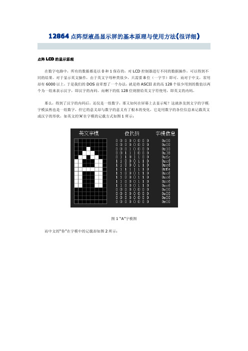
那么,得到了汉字的内码后,还仅是一组数字,那又如何在屏幕上去显示呢?这就涉及到文字的字模,字模虽然也是一组数字,但它的意义却与数字的意义有了根本的变化,它是用数字的各位信息来记载英文或汉字的形状,如英文的'A'在字模的记载方式如图1所示:图1“A”字模图而中文的“你”在字模中的记载却如图2所示:图2“你”字模图12864点阵型LCD简介12864是一种图形点阵液晶显示器,它主要由行驱动器/列驱动器及128×64全点阵液晶显示器组成。
可完成图形显示,也可以显示8×4个(16×16点阵)汉字。
管脚号管脚名称LEVER管脚功能描述1VSS0电源地2VDD+5.0V电源电压3V0-液晶显示器驱动电压4D/I(RS)H/L D/I=“H”,表示DB7∽DB0为显示数据D/I=“L”,表示DB7∽DB0为显示指令数据5R/W H/L R/W=“H”,E=“H”数据被读到DB7∽DB0R/W=“L”,E=“H→L”数据被写到IR或DR 6E H/L R/W=“L”,E信号下降沿锁存DB7∽DB0R/W=“H”,E=“H”DDRAM数据读到DB7∽DB0 7DB0H/L数据线8DB1H/L数据线9DB2H/L数据线10DB3H/L数据线11DB4H/L数据线12DB5H/L数据线13DB6H/L数据线14DB7H/L数据线15CS1H/L H:选择芯片(右半屏)信号16CS2H/L H:选择芯片(左半屏)信号17RET H/L复位信号,低电平复位18VOUT-10V LCD驱动负电压19LED+-LED背光板电源20LED--LED背光板电源表1:12864LCD的引脚说明在使用12864LCD前先必须了解以下功能器件才能进行编程。
大连东福彩色液晶显示器 EDM12832A 模块使用手册说明书

EDM12832A 模块使用手册1.使用范围-------------------------------------------------22.质量保证-------------------------------------------------23.性能特点-------------------------------------------------24.外形图----------------------------------------------------65.I/O接口特性--------------------------------------------66.质量等级-------------------------------------------------157.可靠性-------------------------------------------------178.生产注意事项-------------------------------------------189.使用注意事项-------------------------------------------19LCD 模块使用手册1.使用范围该检验标准适用于大连东福彩色液晶显示器有限公司设计提供的标准液晶显示模块。
如果在使用中出现了异常问题或没有列明的项目,建议同最近的供应商或本公司联系。
2.质量保证如在此手册列明的正常条件下使用、储存该产品,公司将提供12个月的质量保证。
3.性能特点3-1.性能:显示方式 : 反射、正显黄绿色 STN LCD显示颜色 : 显示点: 深蓝色背景: 黄绿色显示形式: 128(w)×32(h) 全点阵输入数据 : 来自MPU的8位并行数据接口Duty驱动路数: 1/32视角: 6 点控制器:KS0108B(Built-in)3-2.机械性能:项目规格单位外形尺寸 110.0(W)×65.0(H) ×10.0 Max.(T) mm显示点阵数 128(W) ×32(H) Dots —视域 76.0(W)×25.0(H) mm显示图形域73.0885(W)×18.2245(H) mm 点间距0.5715(W)×0.5715(H) mm点尺寸0.508(W)×0.508(H) mm78 g重量 Approx.LCD 模块使用手册3-3. 极限参数:项 目 符 号 最小值最大值单位 注 释逻辑 Vdd -0.3 7.0 V电源电压LCD 驱动 Vdd – Vee -0.3 7.0 V输入电压 Vi 0 Vdd V 操作温度 Top 0 50 ℃ 储存温度 Tstg -20 70 ℃ 湿度 — — 90 %RH3-4. 电气特性:3-4-1. 电气参数项 目 符 号 条 件 最小值典型值 最大值 单 位 逻辑 Vdd 4.7 5.0 5.3电源电压LCD 驱动 Vdd–Vee 4.7 — 5.3高电平 Vih Vdd=5V ±5% 0.7Vdd — Vdd输入电压低电平 Vil 0 — 0.3Vdd V高电平 Vih I OH =200UA2.4——输出电压低电平 Vil I 0L=1.6mA —— 0.4 频 率 Fflm Vdd=5V 65 70 75 Hz逻辑 Idd — 10.5 18.0功 耗 LCD 驱动 Iee Vdd=5V Vdd–Vee=5.0VFflm=70HzmA Ta= 0℃φ=0°,θ=0°— 5.2 5.4Ta= 25℃φ=0°,θ=0°4.755.0 5.25 LCD 驱动电压 (推荐电压) Vdd–Vee Ta= 50℃φ=0°,θ=0° 4.6 4.8 —VNote: <1> 驱动路数=1/32 <2> 所有点在静态条件下LCD 模块使用手册3 -5. 电光特性项 目 符号温度 条件 最小值典型值最大值 单位 注释 0℃ — 5.2 5.425℃ 4.75 5.0 5.25LCD 驱动电压(推荐电压)V op 50℃ φ=0°,θ=0° 4.6 4.8 — V 1,2,5 0℃ — 900 1200 上升时间 tr 25℃ — 150 2000℃ — 1200 2500响应 时间衰退时间 td 25℃ φ=0°,θ=0°— 200 250mS 1,3,5垂直 -35 — 35视 角 Δφ 25℃ 水平 -30 — 30deg. 1,4,5对比度 K 25℃ φ=0°,θ=0° 2.0 5.0 — — 1,5,6注意:<1> φ和θ的定义<2> 在此电压范围内能获得对比度大于2(k ≥2)LCD 模块使用手册注意:<4>视角定义注意:<5> 光学测量系统温度控制室(ΔΦ) ΔΦ=|Φ1-Φ2|选择点的亮度(B1)外形图 非选择点的亮度(B2)4.5. I/O 接口特性5-1. I/O 接口表:管脚号 符号 功 能 1 Vee LCD 驱动电压(可调) 2 Vdd 电源电压(+5V) 3 Vss 地(GND)4 E使能信号:当R/W=“L ”,E 下降沿锁存数据线上的数据;当R/W=“H ”,E=“H ”,读DDRAM 的数据到数据线上。
SG12864-01D液晶显示板

说明 液晶显示屏,背光灯箱,线路板,铁框,导电橡胶等 正像反射型,半透型,负像型 STN 型:黄绿模式,灰模式,蓝模式 FSTN 型:黑白模式
单位
6 O’clock
93.00(长)×70.00(宽)×13.00(厚)
mm
70.70(长)×38.80(宽)
(Version 1.0)
LCD 类型 (显示模式) STN 黄绿底色 STN 灰底色 FSTN 黑白正像 STN 黄绿底色 STN 蓝底色
背光类型 (LED) 黄绿底背光
白背光 白背光 黄绿侧背光 白背光
时序方 式
68 时序 68 时序 68 时序 68 时序 68 时序
逻辑电压 (VDD)
5.0V 5.0V 5.0V 5.0V 5.0V
Definition of Contrast Ratio(CR)
Brightness
Driving Voltage
Brightness In Non-Select Signal CR= Brightness In Select Signal
(Positive Type)
Driving Voltage
背光 电压 5.0V 5.0V 5.0V 5.0V 5.0V
接口方式 及其预留配置 单排插针焊位 单排插针焊位 单排插针焊位 单排插针焊位 单排插针焊位
注: 1、 以上列出 LCD 类型为我公司的标准产品,如果有其他需求,请致电我公司销售部
DOC.NO: SG12864-01D
REV: 1.0
-1-
BEIJING ELITE EEM CO..LTD
Address hold time
单片机控制LCD液晶显示器(含程序)
液晶显示器一.实验目的:1.了解全点阵图形LCD的结构和原理掌握在MSP430上如何使用外设。
2.了解LCD显示器的工作原理、种类(笔段型、点阵字符型、点阵图形)及主要性能指标。
3.掌握图形点阵LCD的编程使用方法;理解LCD显示模块命令的种类、功能及使用方法。
4.了解LCD字符生成软件的使用方法(见附录)。
二.实验内容:1.在LCD上显示Hello和中文字“南京工业大学”。
2.通过键盘控制Hello或者中文字符在LCD上左右、上下移动。
3.学会使用字符生成软件来实现任意字符代码的生成和显示。
4.其他另外可以实现的目标:使字符在按键没有松动的情况下连续移动;实现字符的循环移动,即当字符串移动到边界时仍可以移动,显示不完的部分从另一边显示出来。
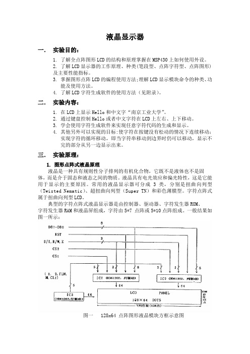
三.实验原理:1.图形点阵式液晶原理液晶是一种具有规则性分子排列的有机化合物,它既不是液体也不是固体,而是介于固态和液态之间的物质。
液晶具有电光效应和偏光特性,这是它能用于显示的主要原因。
常用的液晶显示器可分成3类,分别是扭曲向列型(Twisted Nematic)、超扭曲向列型(Super TN)和彩色薄膜型。
字符点阵式属于扭曲向列型LCD。
典型的字符点阵式液晶显示器是由控制器、驱动器、字符发生器ROM、字符发生器RAM和液晶屏组成,字符由5*7 点阵或5*10点阵组成。
一般结果如图一所示:图一 128x64 点阵图形液晶模块方框示意图此次实验所用的LCD型号是RT12864CT。
12864是一种图形点阵液晶显示器,它主要由行驱动器/列驱动器及128*64全点阵液晶显示器组成。
可完成图形显示,也可以显示8*4个(16*16)汉字。
管脚号管脚名称LEVER 管脚功能描述1 VSS 0 电源地2 VDD +5.0V 电源电压3 V0 - 液晶显示器驱动电压4 D/I(RS) H/L D/I=“H”,表示DB7∽DB0为显示数据D/I=“L”,表示DB7∽DB0为显示指令数据5 R/W H/L R/W=“H”,E=“H”数据被读到DB7∽DB0R/W=“L”,E=“H→L”数据被写到IR或DR6 E H/ R/W=“L”,E信号下降沿锁存DB7∽DB0R/W=“H”,E=“H”DDRAM数据读DB7∽DB07 DB0 H/L 数据线8 DB1 H/L 数据线9 DB2 H/L 数据线10 DB3 H/L 数据线11 DB4 H/L 数据线12 DB5 H/L 数据线13 DB6 H/L 数据线14 DB7 H/L 数据线15 CS1 H/L H:选择芯片(右半屏)信号16 CS2 H/L H:选择芯片(左半屏)信号17 RET H/L 复位信号,低电平复位18 VOUT -10V LCD驱动负电压19 LED+ - LED背光板电源20 LED- - LED背光板电源表1:12864LCD的引脚说明128x64 点阵图形液晶模块的内部结构可分为三个部分:LCD 控制器,LCD 驱动器,LCD 显示装置。
12864点阵型液晶显示屏的基本原理与使用方法(很详细)
0
0
1
1
1
0
0
1
1
X
X
X
0
0
1
0
1
1
1
0
0
0
1
X
X
X
1
0 BUSY 0 ON/OFF RST 0
0
1
写数据
1
1
读数据
DB2 1 X X X 0
DB1 1 X X X 0
DB0 1/0
X X X 0
表 2:12864LCD 指令表
各功能指令分别介绍如下。
显示开/关指令
R/WRS 00
DB7 DB6 DB5 DB4 DB3DB2DB1 DB0 00111111/0
设置了页地址和列地址,就唯一确定了显示 RAM 中的一个单元,这样 MPU 就可以
用读、写指令读出该单元中的内容或向该单元写进一个字节数据。
5、读状态指令
R/WRS 10
DB7 DB6 DB5 DB4 DB3DB2DB1 DB0 BUSY0ON/OFFREST0000
该指令用来查询液晶显示模块内部控制器的状态,各参量含义如下:
图 2 “你”字模图
12864 点阵型 LCD 简介
12864 是一种图形点阵液晶显示器,它主要由行驱动器/列驱动器及 128×64 全点阵液晶显示器组成。 可完成图形显示,也可以显示 8×4 个(16×16 点阵)汉字。
管脚号 1 2 3 4
管脚名称 VSS VDD V0
D/I(RS)
LEVER 0
12864LCD 的指令系统及时序
该类液晶显示模块(即 KS0108B 及其兼容控制驱动器)的指令系统比较简单,总共只有七种。其指 令表如表 2 所示:
基于proteus的模拟信号数字滤波及动态波形输出

智能仪器基础与设计设计报告学院(系):机电工程学院专业:测控技术与仪器学生:指导教师:完成日期 : 2015 年 1 月智能仪器基础与设计基于单片机C语言编程及LCD液晶显示器的数字滤波显示系统设计Design of Digital Filter and Display System Based on Clanguage Programming and Single-Chip Computers基于单片机C语言编程及LCD液晶显示器的数字滤波显示系统设计[摘要]本次实验设计的主要内容是在Proteus仿真环境下,借助单片机和c 语言编程,实现对模拟信号的采集、滤波以及对滤波后信号的LCD动态显示。
本次设计主要采用了三中滤波方式:平均值滤波、中位置滤波、递推平均滤波。
应用的主要器件有:MCS-51单片机,TLC549 8位串行AD,KS0108控制的12864 LCD。
通过对叠加了噪声信号的模拟信号的模数转换实现信号采集,在单片机内部采用函数滤波滤出信号上面叠加的高频噪声,最后通过单片机控制两个LCD分别输出采集到的叠有噪声的信号和滤波后的结果。
[关键字]数字滤波 LCD动态显示 MCS-51 TLC549 KS0108 12864[Abstract]This experiment design is mainly based on the environment of Proteus 8.0, single-chip computer and C language programming. This design managed to collect analog signal, filter signal and dynamic display signal on LCD. In this design, we used 3 diffident filter methods: mean filter; medium filter; recursive average filtering. The devices we used are: MCS-51 single-chip computer; 8-bit serial ADC TLC549; LCD 12864 with its driver KS0108.[Keyword]Digital filtering LCD dynamic display MCS-51 TLC549 KS0108 12864目录1 引言 (5)1.1课题背景介绍 (5)2 各部分器件简单介绍 (6)2.1 MCS-51单片机 (6)2.2 AD转换器TLC549 (7)2.3 LCD液晶显示器12864 (9)3 数字滤波器设计 (10)3.1 数字滤波原理介绍 (10)3.2 单片机电路 (18)3.3 数据采集电路 (19)3.4 显示电路 (19)3.5 总电路 (20)4 程序设计 (21)4.1程序流程图 (21)4.2 总程序关键点解析 (22)4.3 LCD12864驱动子程序 (23)4.4 画坐标子程序 (25)4.5 坐标图字模 (25)4.6 主程序 (27)参考文献 (31)附录 (31)1 引言1.1课题背景介绍1.1数字滤波器的研究背景与意义当今,数字信号处理技术正飞速发展,它不但自成一门学科,更是以不同形式影响和渗透到其他学科:它与国民经济息息相关,与国防建设紧密相连;它影响或改变着我们的生产、生活方式,因此受到人们普遍的关注。
- 1、下载文档前请自行甄别文档内容的完整性,平台不提供额外的编辑、内容补充、找答案等附加服务。
- 2、"仅部分预览"的文档,不可在线预览部分如存在完整性等问题,可反馈申请退款(可完整预览的文档不适用该条件!)。
- 3、如文档侵犯您的权益,请联系客服反馈,我们会尽快为您处理(人工客服工作时间:9:00-18:30)。
INTRODUCTION100 QFP The KS0108B is a LCD driver LSl with 64 channel outputfor dot matrix liquid crystal graphic display system. Thisdevice consists of the display RAM, 64 bit data latch 64 bitdrivers and decoder logics. It has the internal display RAMfor storing the display data transferred from a 8 bit microcontroller and generates the dot matrix Iiquid crystal driv-ing signals corresponding to stored data.The KS0108Bcomposed of the liquid crystal display system in combina-tion with the KS0107B (64 common driver)FEATURES• Dot matrix LCD segment driver with 64 channel output• Input and Output signal- Input: 8 bit parallel display dataControl signal from MPUSplitted bias voltage (V1R, V1L, V2R, V2L,V3R. V3L, V4R, V4L)- Output: 64 channel waveform for LCD driving.• Display data is stored in display data RAM from MPU.• Interface RAM- Capacity: 512 bytes (4096 bits)- RAM bit data: RAM bit data = 1:ONRAM bit data- = 0:OFF• Applicable LCD duty: 1/32~1/64• LCD driving voltage: 8V~17V(V DD-V EE)• Power supply voltage: + 5V±10%Driver ControllerCOMMON SEGMENTKS0107B Other KS0108B MPU• High voltage CMOS process.• 100QFP and bare chip available.Fig.2. 100QFP TopViewADCMV DDV3RV2RV5RV0RV EE2S64S63S62S61S60S59S58S57S56S55S54S53S52S51S50S49S48S47S46S45S44S43DB1DB0V SS V3L V2L V5L V0L V EE1S1S2S3S4S5S6S7S8S9S10S11S12S13S14S15S16S17S18S19S20S21S22S23S24S25S26S27S28S29S30S31S32S33S34S35S36S37S38S39S40S41S42DB2DB3DB4DB5DB6DB7NC NC NC CS3R/W RS CL E FRMPIN DESCIPTIONPIN (NO)SYMBOL INPUT/OUTPUT DESCRIPTION37873, 8V DD V SS V EE1.2Power For internal logic circuit (+5V ±10%)GND (0V)For LCD driver circuitV SS =0V, V DD =5V ¡¾10% V DD -V EE =8V~17VV EE1 and V EE2 is connected by the same voltage.74, 776, 577, 475, 6V0L, V0R V2L, V2R V3L, V3R V5L, V5R Power Bias supply voltage terminals to drive the LCD.929190CS1B CS2B CS3InputChip selectionIn order to interface data for input or outputThe terminals have to be CS1B=L, CS2B=L, and CS3=H.2M Input Alternating signal input for LCD driving.1ADCInputAddress control signal of Y address counter.ADC=H →DB<0:7>=0→Y0→S1 DB<0:7>=63→Y63→S64ADC=L →DB<0:7>=0→Y63→S64 DB<0:7>=63→Y0→S1100FRM InputSynchronous control signal.Presets the 6-bit Z counter and syncronizes the common signal with the frame signal when the frame signal becomes high.99E InputEnable signal.write mode (R/W=L) → data of DB<0:7> is latched at the falling edge of E.read mode (R/W=H) → DB<0:7> appears the reading data while E is at high level.9897CLK1CLK2Input2 phase clock signal for internal operation.Used to execute operations for input/output of display RAM data and others.96CLInputDisplay synchronous signal.Display data is latched at rising time of the CL signal and increments the Z-address counter at the CL falling time.95RS InputData or Instruction.RS=H →DB<0:7> : Display RAM Data RS=L →DB<0:7> : Instruction Data 94R/W InputRead or Write.R/W=H → Data appears at DB<0:7> and can be read by the CPU while E=H, CS1B=L, CS2B=L and CS3=H.R/W=L ¡æDisplay data DB<0:7> can be written at falling of E when CS1B=L, CS2B=L and CS3=H.79~86DB0~DB7Input/OutputData bus.There state I/O common terminal.Select LevelNon-Select Level V0L(R), V5L(R)V2L(R), V3L(R)PIN DESCRIPTION (continued)PIN (NO)NAME INPUT/OUTPUT DESCRIPTION72~9S1~S64Output LCD Segment driver output.Display RAM data 1:ONDisplay RAM data 0:OFF(Relation of display RAM data & M)M DATA Output LevelL L V2H V0H L V3H V593RSTB Input Reset signal.When RSTB=L,(1) ON/OFF register becomes set by 0. (display off)(2) Display start line register becomes set by 0(Z-address 0 set, display from line 0)After releasing reset, this condition can be changed only by instruction.87~89NC No connection.(open)MAXIMUM ABSOLUTE LIMITCharacteristic Symbol Value Unit Note Operating Voltage V DD-0.3~+7.0V*1 Supply Voltage V EE V DD-19.0~V DD+0.3V*4 Driver Supply Voltage V B-0.3~V DD+0.3V*1,3V LCD V EE-0.3~V DD+0.3V*2 Operating Temperature T OPR-30~+85°CStorage Temperature T STG-55~+125°C*1. Based on V SS=0V.*2. Applies the same supply voltage to V EE1 and V EE2. V LCD=V DD-V EE.*3. Applies to M, FRM, CL, RSTB, ADC, CLK1, CLK2, CS1B, CS2B, CS3, E, R/W, RS and DB0~DB7.*4. Applies V0L(R), V2L(R), V3L(R) and V5L(R).Voltage level: V DD≥V0L=VOR≥V2L=V2R≥V3L=V3R≥V5L=V5R≥V EE.ELECTRICAL CHARACTERISTICSDC Characteristics (V DD=4.5~5.5V, V SS=0V, V DD-V EE=8~17V, T a=-30~+85°C)Characteristic Symbol Condition Min Typ Max Unit Note Input High Voltage V IH1-0.7V DD-V DD V*1V IH2- 2.0-V DD V*2 Input Low Voltage V IL1-0-0.3V DD V*1V IL2-0-0.8V*2 Output High Voltage V OH I OH=-200µA 2.4--V*3 Output Low Voltage V OL I OL=1.6mA--0.4V*3 Input Leakage Current I LKG V IN=V SS~V DD-1.0- 1.0µA*4 Three-state(OFF) Input Current I TSL V IN=V SS~V DD-5.0- 5.0µA*5 Driver Input Leakage Current I DIL V IN=V EE~V DD-2.0- 2.0µA*6 Operating Current I DD1During Display--100µA*7--500µA*7I DD2During AccessAccess Cycle=1MHzOn Resistance R ON V DD-V EE=15V--7.5KΩ*8¡¾I LOAD=0.1mA*1. CL, FRM, M, RSTB, CLK1, CLK22. CS1B, CS2B, CS3, E, R/W, RS, DB0~DB73. DB0~DB74. Excepted DB0~DB75. DB0~DB7 at High lmpedance6. V0L(R), V2L(R), V3L(R), V5L(R)7. 1/64 duty, FCLK=250KHZ, Frame Frequency=70HZ, Output: No Load8. V DD~V EE=15.5VV0L(R)>V2L(R)=V DD-2/7 (V DD-V EE)>V3L(R)=V EE+2/7(V DD-V EE)>V5L(R)AC Characteristics (V=5V±10%, V SS=0V, T a=-30°C~+85°C)DD(1) Clock TimingCharacteristic Symbol Min Typ Max Unit CLK1, CLK2 Cycle Time t CY 2.5-20µS CLK1 ‘LOW’ Level Width t WL1625--CLK2 ‘LOW’ Level Width t WL2625--CLK1 ‘HIGH’ Level Width t WH11875--ns CLK2 ‘HIGH’ Level Width t WH21875--CLK1-CLK2 Phase Difference t D12625--CLK2-CLK1 Phase Difference t D21625--CLK1, CLK2 Rise Time t R--150CLK1, CLK2 Fall Time t F--150APPLICATION CIRCUIT1.1/64 duty common driver(KS0107B) interface circuitOPERATING PRINCIPLES & METHODS1. I/O BufferInput buffer controls the status between the enable and disable of chip. Unless the CS1B to CS3 is in active mode, Input or output of data and instruction does not execute. Therefore internal state is not change. But RSTB and ADC can operate regardless CS1B-CS3.2. Input registerInput register is provided to interface with MPU which is different operating frequency. Input register stores the data tempor-arily before writing it into display RAM.When CS1B to CS3 are in the active mode, R/W and RS select the input register. The data from MPU is written into input register. Then Writing it into display RAM. Data latched for falling of the E signal and write automatically into the display data RAM by internal operation.3. Output registerOutput register stores the data temporarily from display data RAM when CS1B, CS2B, CS3 is in active mode and R/W and RS=H, stored data in display data RAM is latched in output register. When CS1B to CS3 is in active mode and R/W=H, RS=L, status data (busy check) can read out.To read the contents of display data RAM, twice access of read instruction is needed. In first access, data in display data RAM is latched into output register. In second access, MPU can read data which is latched. That is, to read the data in display data RAM, it needs dummy read. But status read is not needed dummy read.RS R/W FunctionL L InstructionH Status read (busy check)H L Data write (from input register to display data RAM)H Data read (from display data RAM to output register)4. ResetReset can be initialized system by setting RSTB terminal at low level when turning power on, receiving instruction from MPU. When RSTB becomes low, following procedure is occured.1. Display off2. Display start line register become set by 0.(Z-address 0)While RSTB is low, any instruction except status read can be accepted. Reset status appers at DB4. After DB4 is low, any instruction can be accepted.The Conditions of power supply at initial power up are shown in table 1.5. Busy flagBusy flag indicates that KS0108B is operating or no operating. When busy flag is high, KS0108B is in internal operating. When busy flag is low, KS0108B can accept the data or instruction.DB7 indicates busy flag of the KS0108B.6. Display On/Off Flip-FlopThe display on/off flip-flop makes on/off the liquid crystal display. When flip-flop is reset (logical low), selective voltage or non selective voltage appears on segment output terminals. When flip-flop is set (logic high), non selective voltage appears on segment output terminals regardless of display RAM data.The display on/off flip-flop can changes status by instruction. The display data at all segment disappear while RSTB is low. The status of the flip-flop is output to DB5 by status read instruction.The display on/off flip-flop synchronized by CL signal.7. X Page RegisterX page register designates page of the internal display data RAM.It has not count function. An address is set by instruction.8. Y address counterY address counter designates address of the internal display data RAM. An address is set by instruction and is increasedby 1 automatically by read or write operations of display data.9. Display Data RAMDisplay data RAM stores a display data for liquid crystal display. To express on state dot matrix of liquid crystal display, write data 1. The other way, off state writes 0.Display data RAM address and segment output can be controlled by ADC signal.ADC=H¢¡ DB<0:7>=0 - Y-address 0 - A0 - S1DB<0:7>=63 - Y-address 63 - A63 - S64ADC=L¢¡ DB<0:7>=0 ~ Y-address 63 - A63 - S64DB<0:7>=63 ~ A0 - S1ADC terminal connect the V DD or V SS.10. Display Start Line RegisterThe display start line register indicates of display data RAM to display top line of liquid crystal display.Bit data (DB<0:5>) of the display start line set instruction is latched in display start line register. Latched data is transferredto the Z address counter while FRM is high, presetting the Z address counter.It is used for scrolling of the liquid crystal display screen.DISPLAY CONTROL INSTRUCTIONThe display control instructions control the internal state of the KS0108B. Instruction is received from MPU to KS0108B for the display control. The following table shows various instructions.Instruction RS R/W DB7DB6DB5DB4DB3DB2DB1DB0FunctionDisplay ON/OFF L L L L H H H H H L/H Controls the display onor off. Internal statusand display RAM data isnot affected.L:OFF, H:ONSet Address L L L H Sets the Y address inthe Y address counter.Set Page ( X address)L L H L H H H Sets the X address atthe X address register.Display Start Line L L H H Indicates the displaydata RAM displayed atthe top of the screen.Status Read L H BUSY L ON/OFFRESETL L L L Read status.BUSY L: ReadyH: In operationON/OFF L: Display ONH: Display OFFRESET L: NormalH: ResetWrite Display Data H L Writes data (DB0:7) intodisplay data RAM. Afterwriting intruction, Yaddress is increased by1 automatically.Read Display Data H H Reads data (DB0:7) fromdisplay data RAM to thedata bus.Y address (0~63)Page(0~7)Display start line(0~63)Write DataRead Data2. Timing diagram (1/64 duty)3. LCD Panel interface application circuitPAD DIAGRAMPAD LOCATION PAD NAME PAD NAME PAD NAME PAD NUMBER PAD NUMBER PAD NUMBER COORDINATE COORDINATE COORDINATE Y Y X X Y X 7919161041116613101435155916841809184518451845184518451845184518451845184518451845184518451845184518451845184518451882188218821882188218821882188218821412127711421007882757632507382NC NC NC 245120-5-130-255-380-505-630-755-880-1005S4S3S2S1VEE1V0L V5L V2L V3L VSS DB0DB1DB2DB3DB4DB5DB6DB7CS3CS2B CS1B RSTB R/W RS CL CLK2CLK1E FRM 6970717273747576777879808182838485868788899091929394959697989910035363738394041424344454647484950515253545556575859606162636465666768-1845-1845-1845-1845-1845-1845-1845-1845-1845-1845-1845-1845-1845-1845-1845-1845-1845-1379-1239-1099-959-834-709-584-459-334-209-8441166291416541666-687-562-437-312-187-626218731243756268781293710621187148718821882188218821882188218821882188218821882188218821882188218821882S38S37S36S35S34S33S32S31S30S29S28S27S26S25S24S23S22S21S20S19S18S17S16S15S14S13S12S11S10S9S8S7S6S5184518451845180916841559143413091165104091579066554041529016540-84-209-334-459-584-709-834-959-1099-1239-1379-1845-1845-1845-1845-1845-1140-1275-1410-1882-1882-1882-1882-1882-1882-1882-1882-1882-1882-1882-1882-1882-1882-1882-1882-1882-1882-1882-1882-1882-1882-1882-1882-1882-1882-1487-1187-1062-937-812ADC M VDD V3R V2R V5R V0R VEE2S64S63S62S61S60S59S58S57S56S55S54S53S52S51S50S49S48S47S46S45S44S43S42S41S40S3912345678910111213141516171819202122232425262728293031323334。