SN74ALS541DWG4,SN74ALS541-1DWG4,SN74ALS541-1DBRG4,SN74ALS541-1DWRG4, 规格书,Datasheet 资料
74hc541中文资料

74HC541 8路缓冲器/线路驱动器具备74HC240所有的功能,并且把输入引脚和输出引脚分布在封装的两边,这就极大方便了印刷电路板的布线。
1.74hc541中文资料
74HC541 8路缓冲器/线路驱动器具备74HC240所有的功能,并且把输入引脚和输出引脚分布在封装的两边,这就极大方便了印刷电路板的布线。
74HC541的三态输出由一个两输入或非门控制。
当任一个输出使能端(OE1或OE2)为高时,八个输出端将进入高阻态。
74HC541器件的输出为原码数据。
该7HC/HCT54是八进制非反相缓冲器/线路,具有三态输出的驱动器。
三态输出是由输出使能输入OE1和OE2控制。
OEN高导致输出呈现高电平。
阻抗呈关闭状态,“541”与“540”相同,但具有非反相输出。
2.74hc541引脚图及功能
SN74HC541能够完成两侧输入的封装和输引脚的排列与输出的功能,通俗的说,就是可以完成三态输出的八线路缓冲器和线路驱动器。
SN54HC541引脚配置和功能
OE1 :输出使能(低电平有效)两个OE必须为低电平才能使能输出
A1:通道1输入,A2 :通道2输入,A3:通道3输入,A4:通道4输入,A5:通道5输入,A6:通道6输入,A7:通道7输入,A8:通道8输入。
GND:【地】
Y8 :通道8输出,Y7 :通道7输出,Y6 :通道6输出,Y5 :通道5输出,Y4 :通道4输出,Y3 :通道3输出,Y2 :通道2输出,Y1 :通道1输出。
OE2 :输出使能(低电平有效)OE必须为低电平才能使能输出。
VCC :电源引脚。
单路反相器SN74LVC1G04

FUNCTION TABLE
INPUT A
OUTPUT Y
H
L
L
H
LOGIC DIAGRAM (POSITIVE LOGIC) (DBV, DCK, DRL, DRY, DSF, AND YZP PACKAGE)
2 A
4 Y
LOGIC DIAGRAM (POSITIVE LOGIC) (YZV PACKAGE)
SOT (SOT-553) – DRL
Reel of 4000 SN74LVC1G04DRLR
TOP-SIDE MARKING(3) _ _ _ CC_ _ _ _ CC_ CC CC C04_
CC_
(1) Package drawings, thermal data, and symbolization are available at /packaging. (2) For the most current package and ordering information, see the Package Option Addendum at the end of this document, or see the TI
116
DSF package
300
Tstg
Storage temperature range
–65
150 °C
(1) Stresses beyond those listed under "absolute maximum ratings" may cause permanent damage to the device. These are stress ratings only, and functional operation of the device at these or any other conditions beyond those indicated under "recommended operating conditions" is not implied. Exposure to absolute-maximum-rated conditions for extended periods may affect device reliability.
74hc541

74hc54174HC541是一种集成电路芯片,属于高速CMOS逻辑器件。
本文档将详细介绍74HC541的特点、工作原理及常见应用场景。
1. 74HC541 简介74HC541是一种具有8个非反相输入和8个非反相输出的八位三态缓冲器。
它具有高速操作、广泛的工作电压范围以及可靠性强等特点。
该器件可以通过输入引脚控制输出信号的使能与禁止,以实现数据的缓冲和传输。
2. 74HC541的工作原理74HC541的工作原理基于三态门的操作方式。
它包含八个相互独立的缓冲器,每个缓冲器都有一个输入引脚和一个输出引脚。
当输入引脚为高电平时,输出引脚会跟随输入引脚的电平。
当输入引脚为低电平时,输出引脚会保持高阻态,即输出信号不会受到影响。
这种使能与禁止输出的能力使得74HC541在数据传输中非常有用。
3. 74HC541的特点3.1 高速操作:74HC541具有快速响应的特点,适用于高速数据传输和缓冲操作。
3.2 宽工作电压范围:74HC541可以在2V至6V的工作电压范围内正常工作,因此非常适用于不同的电路设计和项目需求。
3.3 低功耗:74HC541的设计采用了低功耗CMOS技术,能够在保证高性能的同时降低功耗。
3.4 八位三态缓冲器:74HC541提供了八个独立的缓冲器,每个缓冲器具有使能功能,方便数据传输和控制。
3.5 耐电磁干扰性能:74HC541采用了抗电磁干扰设计,能够在电磁环境干扰下正常工作。
4. 74HC541的应用场景4.1 数据总线缓冲器:74HC541常用于处理数据总线缓冲,可以提供数据传输和缓冲功能,保证数据的稳定性和可靠性。
4.2 时序控制器:74HC541可以作为时序控制器的一部分,用于控制各个信号的传输和缓冲,确保正确的时序顺序。
4.3 电平转换器:74HC541还可以用作电平转换器,将不同电平的信号转换为兼容的电平,方便不同电路之间的连接和通信。
4.4 数据缓冲和传输:由于74HC541具有快速响应和三态缓冲功能,因此在需要进行数据缓冲和传输的应用中非常常见,例如数据存储器、寄存器等。
DM74ALS541WM资料
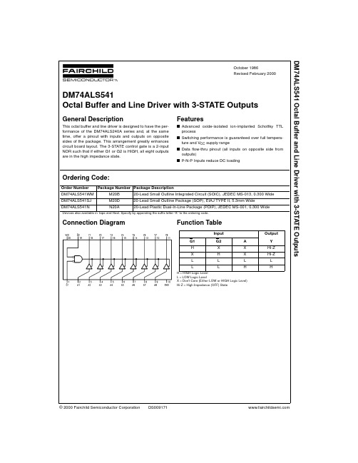
© 2000 Fairchild Semiconductor Corporation DS009171October 1986Revised February 2000DM74ALS541 Octal Buffer and Line Driver with 3-STATE OutputsDM74ALS541Octal Buffer and Line Driver with 3-STATE OutputsGeneral DescriptionThis octal buffer and line driver is designed to have the per-formance of the DM74ALS240A series and, at the same time, offer a pinout with inputs and outputs on opposite sides of the package. This arrangement greatly enhances circuit board layout. The 3-STATE control gate is a 2-input NOR such that if either G1 or G2 is HIGH, all eight outputs are in the high impedance state.Featuress Advanced oxide-isolated ion-implanted Schottky TTL process s Switching performance is guaranteed over full tempera-ture and V CC supply range s Data flow-thru pinout (all inputs on opposite side from outputs)s P-N-P Inputs reduce DC loadingOrdering Code:Devices also available in T ape and Reel. Specify by appending the suffix letter “X” to the ordering code.Connection Diagram Function TableH = HIGH Logic Level L = LOW Logic LevelX = Don't Care (Either LOW or HIGH Logic Level)Hi-Z = High Impedance (OFF) StateOrder Number Package Number Package DescriptionDM74ALS541WM M20B 20-Lead Small Outline Integrated Circuit (SOIC), JEDEC MS-013, 0.300 Wide DM74ALS541SJ M20D 20-Lead Small Outline Package (SOP), EIAJ TYPE II, 5.3mm Wide DM74ALS541NN20A20-Lead Plastic Dual-In-Line Package (PDIP), JEDEC MS-001, 0.300 WideInputOutput G1G2A Y H X X Hi-Z X H X Hi-Z L L L L LLHH 2D M 74A L S 541Absolute Maximum Ratings (Note 1)Note 1: The “Absolute Maximum Ratings” are those values beyond which the safety of the device cannot be guaranteed. The device should not be operated at these limits. The parametric values defined in the Electrical Characteristics tables are not guaranteed at the absolute maximum ratings.The “Recommended Operating Conditions” table will define the conditions for actual device operation.Recommended Operating ConditionsElectrical Characteristicsover recommended free air temperature range Supply Voltage7V Input Voltage: Control Inputs 7VVoltage Applied to a Disabled 3-STATE Output5.5VOperating Free-Air Temperature Range 0°C to +70°C Storage Temperature Range −65°C to +150°CTypical θJA N Package 58.5°C/W M Package77.5°C/WSymbol ParameterMin Nom Max Units V CC Supply Voltage4.555.5V V IH HIGH Level Input Voltage 2V V IL LOW Level Input Voltage 0.8V I OH HIGH Level Output Current −15mA I OL LOW Level Output Current 24mA T AFree Air Operating Temperature70°CSymbol ParameterTest ConditionsMinTypMax Units V IK Input Clamp Voltage V CC = Min, I I = −18 mA −1.2VV OHHIGH Level V CC = 4.5V to 5.5V I OH = −0.4 mA V CC − 2Output VoltageV CC = MinI OH = −3 mA 2.4 3.2VI OH = Max2V OL LOW Level V CC = Min I OL = 12 mA 0.250.4mA Output VoltageI OL = 24 mA0.350.5I I Input Current at Maximum V CC = Max, V I = 7V 100µA Input VoltageI IH HIGH Level Input Current V CC = Max, V I = 2.7V 20µA I IL LOW Level Input Current V CC = Max, V I = 0.4V −100µA I OZH HIGH Level 3-STATE V CC = Max, V O = 2.7V 20µA Output Current I OZL LOW Level 3-STATE V CC = Max, V O = 0.4V −20µA Output Current I O Output Drive Current V CC = Max, V O = 2.25V −30−112mAI CCSupply CurrentV CC = MaxOutputs HIGH 614Outputs LOW 1525mA Outputs Disabled13.522DM74ALS541Switching Characteristicsover recommended operating free air temperature range Symbol ParameterConditionsFrom (Input)Min Max Units To (Output)t PLH Propagation Delay Time V CC = 4.5V to 5.5V, A to Y 414ns LOW-to-HIGH Level Output R 1 = R 2 = 500Ω,t PHL Propagation Delay Time C L = 50 pFA to Y 210ns HIGH-to-LOW Level Output t PZH Output Enable Time G to Y 515ns to HIGH Level Output t PZL Output Enable Time G to Y 820ns to LOW Level Output t PHZ Output Disable Time G to Y 110ns from HIGH Level Output t PLZOutput Disable Time G to Y212nsfrom LOW Level Output 4D M 74A L S 541Physical Dimensionsinches (millimeters) unless otherwise noted20-Lead Small Outline Integrated Circuit (SOIC), JEDEC MS-013, 0.300 WidePackage Number M20B DM74ALS541Physical Dimensions inches (millimeters) unless otherwise noted (Continued)20-Lead Small Outline Package (SOP), EIAJ TYPE II, 5.3mm WidePackage Number M20D6D M 74A L S 541 O c t a l B u f f e r a n d L i n e D r i v e r w i t h 3-S T A TE O u t p u t sPhysical Dimensions inches (millimeters) unless otherwise noted (Continued)20-Lead Plastic Dual-In-Line Package (PDIP), JEDEC MS-001, 0.300 WidePackage Number N20AFairchild does not assume any responsibility for use of any circuitry described, no circuit patent licenses are implied and Fairchild reserves the right at any time without notice to change said circuitry and specifications.LIFE SUPPORT POLICYFAIRCHILD’S PRODUCTS ARE NOT AUTHORIZED FOR USE AS CRITICAL COMPONENTS IN LIFE SUPPORT DEVICES OR SYSTEMS WITHOUT THE EXPRESS WRITTEN APPROVAL OF THE PRESIDENT OF FAIRCHILD SEMICONDUCTOR CORPORATION. As used herein:1.Life support devices or systems are devices or systems which, (a) are intended for surgical implant into the body, or (b) support or sustain life, and (c) whose failure to perform when properly used in accordance with instructions for use provided in the labeling, can be rea-sonably expected to result in a significant injury to the user. 2. A critical component in any component of a life support device or system whose failure to perform can be rea-sonably expected to cause the failure of the life support device or system, or to affect its safety or effectiveness.。
74AHCT541BQ资料

74AHC_AHCT541_3
Product data sheet
Rev. 03 — 12 November 2007
© NXP B.V. 2007. All rights reserved.
4 of 16
元器件交易网
NXP Semiconductors
74AHC541; 74AHCT541
74AHC_AHCT541_3
Product data sheet
Rev. 03 — 12 November 2007
© NXP B.V. 2007. All rights reserved.
2 of 16
元器件交易网
NXP Semiconductors
74AHC541; 74AHCT541
V V V °C ns/V ns/V
Table 6. Static characteristics Voltages are referenced to GND (ground = 0 V).
Symbol Parameter Conditions
25 °C
−40 °C to +85 °C −40 °C to +125 °C Unit
6. Functional description
Table 3. Control OE0 L L X H
Functional table[1]
OE1 L L H X
[1] H = HIGH voltage level; L = LOW voltage level; X = don’t care; Z = high-impedance OFF-state.
Min Typ Max Min Max
Min
sn74 74

74LS属于TTL类型的集成电路,而74HC属于CMOS集成电路。
LS、HC 二者高电平低电平定义不同,HC高电平规定为0.7倍电源电压,低电平规定为0.3倍电源电压。
LS规定高电平为2.0V,低电平为0.8V。
带负载特性不同。
HC上拉下拉能力相同,LS 上拉弱而下拉强。
输入特性不同。
HC输入电阻很高,输入开路时电平不定。
LS输入内部有上拉,输入开路时为高电平。
(1)74LS系列是“低功耗肖特基TTL”,统称74LS系列。
其改进型为“先进低功耗肖特基TTL”,既74ALS系列,它的性能比74LS更好。
(2)74HC系列,它具有CMOS的低功耗和相当于74LS高速度的性能,属于一种高速低功耗产品。
(3)上述两者的工作频率都在30mHz以下,74ALS略高,可达50mHz。
(4)但它们的工作电压却大不相同:74LS系列为5V,74HC系列为2~6V。
(5)扇出能力:74LS系列为20,而74HC系列在直流时则高达1000以上,但在交流时很低,由工作频率决定74HC属于CMOS系列,输入阻抗高,输出电压高(4.9V为逻辑1),驱动能力差;74LS属于TTL系列,输出电压较低(3.5V为逻辑1),驱动能力较强;与单片机匹配,关系不大,但尽量用同一类型的芯片,即74HC 系列74系列芯片功能大全7400 TTL 2输入端四与非门7401 TTL 集电极开路2输入端四与非门7402 TTL 2输入端四或非门7403 TTL 集电极开路2输入端四与非门7404 TTL 六反相器7405 TTL 集电极开路六反相器7406 TTL 集电极开路六反相高压驱动器7407 TTL 集电极开路六正相高压驱动器7408 TTL 2输入端四与门7409 TTL 集电极开路2输入端四与门7410 TTL 3输入端3与非门74107 TTL 带清除主从双J-K触发器74109 TTL 带预置清除正触发双J-K触发器7411 TTL 3输入端3与门74112 TTL 带预置清除负触发双J-K触发器7412 TTL 开路输出3输入端三与非门74121 TTL 单稳态多谐振荡器74122 TTL 可再触发单稳态多谐振荡器74123 TTL 双可再触发单稳态多谐振荡器74125 TTL 三态输出高有效四总线缓冲门74126 TTL 三态输出低有效四总线缓冲门7413 TTL 4输入端双与非施密特触发器74132 TTL 2输入端四与非施密特触发器74133 TTL 13输入端与非门74136 TTL 四异或门74138 TTL 3-8线译码器/复工器74139 TTL 双2-4线译码器/复工器7414 TTL 六反相施密特触发器74145 TTL BCD—十进制译码/驱动器7415 TTL 开路输出3输入端三与门74150 TTL 16选1数据选择/多路开关74151 TTL 8选1数据选择器74153 TTL 双4选1数据选择器74154 TTL 4线—16线译码器74155 TTL 图腾柱输出译码器/分配器74156 TTL 开路输出译码器/分配器74157 TTL 同相输出四2选1数据选择器74158 TTL 反相输出四2选1数据选择器7416 TTL 开路输出六反相缓冲/驱动器74160 TTL 可预置BCD异步清除计数器74161 TTL 可予制四位二进制异步清除计数器74162 TTL 可预置BCD同步清除计数器74163 TTL 可予制四位二进制同步清除计数器74164 TTL 八位串行入/并行输出移位寄存器74165 TTL 八位并行入/串行输出移位寄存器74166 TTL 八位并入/串出移位寄存器74169 TTL 二进制四位加/减同步计数器7417 TTL 开路输出六同相缓冲/驱动器74170 TTL 开路输出4×4寄存器堆74173 TTL 三态输出四位D型寄存器74174 TTL 带公共时钟和复位六D触发器74175 TTL 带公共时钟和复位四D触发器74180 TTL 9位奇数/偶数发生器/校验器74181 TTL 算术逻辑单元/函数发生器74185 TTL 二进制—BCD代码转换器74190 TTL BCD同步加/减计数器74191 TTL 二进制同步可逆计数器74192 TTL 可预置BCD双时钟可逆计数器74193 TTL 可预置四位二进制双时钟可逆计数器74194 TTL 四位双向通用移位寄存器74195 TTL 四位并行通道移位寄存器74196 TTL 十进制/二-十进制可预置计数锁存器74197 TTL 二进制可预置锁存器/计数器7420 TTL 4输入端双与非门7421 TTL 4输入端双与门7422 TTL 开路输出4输入端双与非门74221 TTL 双/单稳态多谐振荡器74240 TTL 八反相三态缓冲器/线驱动器74241 TTL 八同相三态缓冲器/线驱动器74243 TTL 四同相三态总线收发器74244 TTL 八同相三态缓冲器/线驱动器74245 TTL 八同相三态总线收发器74247 TTL BCD—7段15V输出译码/驱动器74248 TTL BCD—7段译码/升压输出驱动器74249 TTL BCD—7段译码/开路输出驱动器74251 TTL 三态输出8选1数据选择器/复工器74253 TTL 三态输出双4选1数据选择器/复工器74256 TTL 双四位可寻址锁存器74257 TTL 三态原码四2选1数据选择器/复工器74258 TTL 三态反码四2选1数据选择器/复工器74259 TTL 八位可寻址锁存器/3-8线译码器7426 TTL 2输入端高压接口四与非门74260 TTL 5输入端双或非门74266 TTL 2输入端四异或非门7427 TTL 3输入端三或非门74273 TTL 带公共时钟复位八D驱动器74279 TTL 四图腾柱输出S-R锁存器7428 TTL 2输入端四或非门缓冲器74283 TTL 4位二进制全加器74290 TTL 二/五分频十进制计数器74293 TTL 二/八分频四位二进制计数器74295 TTL 四位双向通用移位寄存器74298 TTL 四2输入多路带存贮开关74299 TTL 三态输出八位通用移位寄存器7430 TTL 8输入端与非门7432 TTL 2输入端四或门74322 TTL 带符号扩展端八位移位寄存器74323 TTL 三态输出八位双向移位/存贮寄存器7433 TTL 开路输出2输入端四或非缓冲器74347 TTL BCD—7段译码器/驱动器74352 TTL 双4选1数据选择器/复工器74353 TTL 三态输出双4选1数据选择器/复工器74365 TTL 门使能输入三态输出六同相线驱动器74365 TTL 门使能输入三态输出六同相线驱动器74366 TTL 门使能输入三态输出六反相线驱动器74367 TTL 4/2线使能输入三态六同相线驱动器74368 TTL 4/2线使能输入三态六反相线驱动器7437 TTL 开路输出2输入端四与非缓冲器74373 TTL 三态同相八D锁存器74374 TTL 三态反相八D锁存器74375 TTL 4位双稳态锁存器74377 TTL 单边输出公共使能八D锁存器74378 TTL 单边输出公共使能六D锁存器74379 TTL 双边输出公共使能四D锁存器7438 TTL 开路输出2输入端四与非缓冲器74380 TTL 多功能八进制寄存器7439 TTL 开路输出2输入端四与非缓冲器74390 TTL 双十进制计数器74393 TTL 双四位二进制计数器7440 TTL 4输入端双与非缓冲器7442 TTL BCD—十进制代码转换器74352 TTL 双4选1数据选择器/复工器74353 TTL 三态输出双4选1数据选择器/复工器74365 TTL 门使能输入三态输出六同相线驱动器74366 TTL 门使能输入三态输出六反相线驱动器74367 TTL 4/2线使能输入三态六同相线驱动器74368 TTL 4/2线使能输入三态六反相线驱动器7437 TTL 开路输出2输入端四与非缓冲器74373 TTL 三态同相八D锁存器74374 TTL 三态反相八D锁存器74375 TTL 4位双稳态锁存器74377 TTL 单边输出公共使能八D锁存器74378 TTL 单边输出公共使能六D锁存器74379 TTL 双边输出公共使能四D锁存器7438 TTL 开路输出2输入端四与非缓冲器74380 TTL 多功能八进制寄存器7439 TTL 开路输出2输入端四与非缓冲器74390 TTL 双十进制计数器74393 TTL 双四位二进制计数器7440 TTL 4输入端双与非缓冲器7442 TTL BCD—十进制代码转换器74447 TTL BCD—7段译码器/驱动器7445 TTL BCD—十进制代码转换/驱动器74450 TTL 16:1多路转接复用器多工器74451 TTL 双8:1多路转接复用器多工器74453 TTL 四4:1多路转接复用器多工器7446 TTL BCD—7段低有效译码/驱动器74460 TTL 十位比较器74461 TTL 八进制计数器74465 TTL 三态同相2与使能端八总线缓冲器74466 TTL 三态反相2与使能八总线缓冲器74467 TTL 三态同相2使能端八总线缓冲器74468 TTL 三态反相2使能端八总线缓冲器74469 TTL 八位双向计数器7447 TTL BCD—7段高有效译码/驱动器7448 TTL BCD—7段译码器/内部上拉输出驱动74490 TTL 双十进制计数器74491 TTL 十位计数器74498 TTL 八进制移位寄存器7450 TTL 2-3/2-2输入端双与或非门74502 TTL 八位逐次逼近寄存器74503 TTL 八位逐次逼近寄存器7451 TTL 2-3/2-2输入端双与或非门74533 TTL 三态反相八D锁存器74534 TTL 三态反相八D锁存器7454 TTL 四路输入与或非门74540 TTL 八位三态反相输出总线缓冲器7455 TTL 4输入端二路输入与或非门74563 TTL 八位三态反相输出触发器74564 TTL 八位三态反相输出D触发器74573 TTL 八位三态输出触发器74574 TTL 八位三态输出D触发器74645 TTL 三态输出八同相总线传送接收器74670 TTL 三态输出4×4寄存器堆7473 TTL 带清除负触发双J-K触发器7474 TTL 带置位复位正触发双D触发器7476 TTL 带预置清除双J-K触发器7483 TTL 四位二进制快速进位全加器7485 TTL 四位数字比较器7486 TTL 2输入端四异或门7490 TTL 可二/五分频十进制计数器7493 TTL 可二/八分频二进制计数器7495 TTL 四位并行输入\输出移位寄存器7497 TTL 6位同步二进制乘法器SN74LSOOSN74LSOO 四2输入与非门SN74LSO2 四2输入与非门SN74LS04 六反相器SN74LS06 六反相缓冲器/驱动器SN74LS08 四2输入与非门SN74LS10 三3输入与非门SN74LS12 三3输入与非门SN74LS14 六反相器.斯密特触发SN74LS16 六反相缓冲器/触发器SN74LS20 双4输入与门SN74LS22 双4输入与门SN74LS26 四2输入与非门SN74LS28 四输入端或非缓冲器SN74LS32 四2输入或门SN74LS37 四输入端与非缓冲器SN74LS40 四输入端与非缓冲器SN74LS47 BCD-七段译码驱动器SN74LS49 BCD-七段译码驱动器SN74LS54 四输入与或非门SN74LS63 六电流读出接口门SN74LS74 双D触发器SN74LS76 双J-K触发器SN74LS83 双J-K触发器SN74LS86 四2输入异或门SN74LS90 4位十进制波动计数器SN74LS92 12分频计数器SN74LS96 5位移位寄存器SN74LS109 正沿触发双J-K触发器SN74LS113 双J-K负沿触发器SN74LS121 单稳态多谐振荡器SN74LS123 双稳态多谐振荡器SN74LS125 三态缓冲器SN74LS131 3-8线译码器SN74LS133 13输入与非门SN74LS137 地址锁存3-8线译码器SN74LS139 双2-4线译码-转换器SN74LS147 10-4线优先编码器SN74LS153 双4选1数据选择器SN74LS155 双2-4线多路分配器SN74LS157 四2选1数据选择器SN74LS160 同步BDC十进制计数器SN74LS162 同步BDC十进制计数器SN74LS164 8位串入并出移位寄存SN74LS166 8位移位寄存器SN74LS169 4位可逆同步计数器SN74LS172 16位多通道寄存器堆SN74LS174 6D型触发器SN74LS176 可预置十进制计数器SN74LS182 超前进位发生器SN74LS189 64位随机存储器SN74LS191 二进制同步可逆计数器SN74LS193 二进制可逆计数器SN74LS195 并行存取移位寄存器SN74LS197 可预置二进制计数器SN74LS238 3-8线译码/多路转换器SN74LS241 八缓冲/驱动/接收器SN74LS243 四总线收发器SN74LS245 八总线收发器SN74LS248 BCD-七段译码驱动器SN74LS251 三态8-1数据选择器SN74LS256 双四位选址锁存器SN74LS258 四2选1数据选择器SN74LS260 双5输入或非门SN74LS266 四2输入异或非门SN74LS275 七位树型乘法器SN74LS279 四R-S触发器SN74LS283 4位二进制全加器SN74LS293 4位二进制计数器SN74LS365 六缓冲器带公用启动器SN74LS367 六总线三态输出缓冲器SN74LS373 8D锁存器SN74LS375 4位双稳锁存器SN74LS386 四2输入异或门SN74LS393 双4位二进制计数器SN74LS574 8位D型触发器SN74LS684 8位数字比较器SN74LSO1 四2输入与非门SN74LS03 四2输入与非门SN74LS05 六反相器SN74LS07 六缓冲器/驱动器SN74LS09 四2输入与非门SN74LS11 三3输入与非门SN74LS13 三3输入与非门SN74LS15 三3输入与非门SN74LS17 六反相缓冲器/驱动器SN74LS21 双4输入与门SN74LS25 双4输入与门SN74LS27 三3输入与非门SN74LS30 八输入端与非门SN74LS33 四2输入或门SN74LS38 双2输入与非缓冲器SN74LS42 BCD-十进制译码器SN74LS48 BCD-七段译码驱动器SN74LS51 三3输入双与或非门SN74LS55 四4输入与或非门SN74LS73 双J-K触发器SN74LS75 4位双稳锁存器SN74LS78 双J-K触发器SN74LS85 4位幅度比较器SN74LS88 4位全加器SN74LS91 8位移位寄存器SN74LS93 二进制计数器SN74LS95 4位并入并出寄存器SN74LS107 双J-K触发器SN74LS112 双J-K负沿触发器SN74LS114 双J-K负沿触发器SN74LS122 单稳态多谐振荡器SN74LS124 双压控振荡器SN74LS126 四3态总线缓冲器SN74LS132 二输入与非触发器SN74LS136 四异或门SN74LS138 3-8线译码/转换器SN74LS145 BCD十进制译码/驱动器SN74LS148 8-3线优先编码器SN74LS151 8选1数据选择器SN74LS154 4-16线多路分配器SN74LS156 双2-4线多路分配器SN74LS158 四2选1数据选择器SN74LS161 4位二进制计数器SN74LS163 4位二进制计数器SN74LS165 8位移位寄存器SN74LS168 4位可逆同步计数器SN74LS170 4x4位寄存器堆SN74LS173 4D型寄存器SN74LS175 4D烯触发器SN74LS181 运算器/函数发生器SN74LS183 双进位保存全价器SN74LS190 同步BCD十进制计数器SN74LS192 BCD-同步可逆计数器SN74LS194 双向通用移位寄存器SN74LS196 可预置十进制计数器SN74LS221 双单稳态多谐振荡器SN74LS240 八缓冲/驱动/接收器SN74LS242 四总线收发器SN74LS244 八缓冲/驱动/接收器SN74LS247 BCD-七段译码驱动器SN74LS249 BCD-七段译码驱动器SN74LS253 双三态4-1数据选择器SN74LS257 四3态2-1数据选择器SN74LS259 8位可寻址锁存器SN74LS261 2x4位二进制乘发器SN74LS273 八进制D型触发器SN74LS276 四J-K触发器SN74LS280 9位奇偶数发生校检器SN74LS290 十进制计数器SN74LS295 4位双向通用移位寄存器SN74LS366 六缓冲器带公用启动器SN74LS368 六总线三态输出反相器SN74LS374 8D触发器SN74LS377 8位单输出D型触发器SN74LS390 双十进制计数器SN74LS573 8位三态输出D型锁存器SN74LS670 8位数字比较器SN74HC00 四2输入与非门SN74HC02 四2输入或非门SN74HC03 四2输入或非门SN74HC04 六反相器SN74HC05 六反相器SN74HC08 四2输入与门SN74HC10 三3输入与非门SN74HC11 三3输入与门SN74HC14 六反相器/斯密特触发器SN74HC20 双四输入与门SN74HC21 双四输入与非门SN74HC27 三3输入与非门SN74HC30 八输入端与非门SN74HC32 四2输入或门SN74HC42 BCD十进制译码器SN74HC73 双J-K触发器SN74HC74 双D型触发器SN74HC76 双J-K触发器SN74HC86 四2输入异或门SN74HC107 双J-K触发器SN74HC113 双J-K负沿触发器SN74HC123 双稳态多谐振荡器SN74HC125 三态缓冲器SN74HC126 四三态总线缓冲器SN74HC132 二输入与非缓冲器SN74HC137 二输入与非缓冲器SN74HC138 3-8线译码/解调器SN74HC139 双2-4线译码/解调器SN74HC148 8选1数据选择器SN74HC151 双4选1数据选择器SN74HC154 4-16线多路分配器SN74HC157 四2选1数据选择器SN74HC161 4位二进制计数器SN74HC163 4位二进制计数器SN74HC164 8位串入并出移位寄存器SN74HC165 8位移位寄存器SN74HC173 4D型触发器SN74HC174 6D触发器SN74HC175 4D型触发器SN74HC191 二进制同步可逆计数器SN74HC221 双单稳态多谐振荡器SN74HC238 3-8线译码器SN74HC240 八缓冲器SN74HC244 八总线3态输出缓冲器SN74HC245 八总线收发器SN74HC251 三态8-1数据选择器SN74HC259 8位可寻址锁存器SN74HC266 四2输入异或非门SN74HC273 8D型触发器SN74HC367 六缓冲器/总线驱动器SN74HC368 六缓冲器/总线驱动器SN74HC373 8D锁存器SN74HC374 8D触发器SN74HC393 双4位二进制计数器SN74HC541 8位三态输出缓冲器SN74HC573 8位三态输出D型锁存器SN74HC574 8D型触发器SN74HC595 8位移位寄存器/锁存器SN74HC4028 7级二进制串行加数器SN74HC4046 锁相环SN74HC4050 六同相缓冲器SN74HC4051 8选1模拟开关SN74HC4053 三2选1模拟开关SN74HC4060 14位计数/分频/振荡器SN74HC4066 四双相模拟开关SN74HC4078 3输入端三或门SN74HC4511 7段锁存/译码驱动器SN74HC4520 双二进制加法计数器74F00 高速四2输入与非门74F02 高速四2输入或非门74F04 高速六反相器74F08 高速四2输入与门74F10 高速三3输入与门74F14 高速六反相斯密特触发74F32 高速四2输入或门74F38 高速四2输入或门74F74 高速双D型触发器74F86 高速四2输入异或门74F139 高速双2-4线译码/驱动器74F151 高速双2-4线译码/驱动器74F153 高速双4选1数据选择器74F157 高速双4选1数据选择器74F161 高速6D型触发器74F174 高速6D型触发器74F175 高速4D型触发器74F244 高速八总线3态缓冲器74F245 高速八总线收发器74F373 高速8D锁存器SN74HCT04 六反相器常用74系列标准数字电路的中文名称资料器件代号器件名称74 74LS74HC00 四2输入端与非门√ √ √01 四2输入端与非门(OC) √√02 四2输入端或非门√ √ √03 四2输入端与非门(OC) √√04 六反相器√ √ √05 六反相器(OC) √ √06 六高压输出反相器(OC,30V) √ √07 六高压输出缓冲,驱动器(OC,30V) √ √ √08 四2输入端与门√ √ √09 四2输入端与门(OC) √ √√10 三3输入端与非门√ √ √11 三3输入端与门√ √12 三3输入端与非门(OC) √√ √13 双4输入端与非门√ √ √14 六反相器√ √ √15 三3输入端与门(OC) √ √16 六高压输出反相器(OC,15V) √17 六高压输出缓冲,驱动器(OC,15V) √20 双4输入端与非门√ √ √21 双4输入端与门√ √ √22 双4输入端与非门(OC) √√25 双4输入端或非门(有选通端) √ √ √26 四2输入端高压输出与非缓冲器√ √ √27 三3输入端或非门√ √ √28 四2输入端或非缓冲器√ √ √30 8输入端与非门√ √ √32 四2输入端或门√ √ √33 四2输入端或非缓冲器(OC) √ √37 四2输入端与非缓冲器√ √38 四2输入端与非缓冲器(OC) √ √40 双4输入端与非缓冲器√ √ √42 4线-10线译码器(BCD输入) √ √43 4线-10线译码器(余3码输入) √44 4线-10线译码器(余3葛莱码输入) √48 4线-7段译码器√49 4线-7段译码器√50 双2路2-2输入与或非门√ √ √51 2路3-3输入,2路2-2输入与或非门√ √ √52 4路2-3-2-2输入与或门√53 4路2-2-2-2输入与或非门√54 4路2-3-3-2输入与或非门√ √55 2路4-4输入与或非门√60 双4输入与扩展器√ √61 三3输入与扩展器√62 4路2-3-3-2输入与或扩展器√64 4路4-2-3-2输入与或非门√65 4路4-2-3-2输入与或非门(OC) √70 与门输入J-K触发器√71 与或门输入J-K触发器√72 与门输入J-K触发器√74 双上升沿D型触发器√ √78 双D型触发器√ √85 四位数值比较器√86 四2输入端异或门√ √ √87 4位二进制原码/反码√95 4位移位寄存器√101 与或门输入J-K触发器√102 与门输入J-K触发器√107 双主-从J-K触发器√108 双主-从J-K触发器√109 双主-从J-K触发器√110 与门输入J-K触发器√111 双主-从J-K触发器√ √112 双下降沿J-K触发器√113 双下降沿J-K触发器√114 双下降沿J-K触发器√116 双4位锁存器√120 双脉冲同步驱动器√121 单稳态触发器√ √ √122 可重触发单稳态触发器√ √ √123 可重触发双稳态触发器√ √ √125 四总线缓冲器√ √ √126 四总线缓冲器√ √ √128 四2输入端或非线驱动器√ √ √132 四2输入端与非门√ √ √。
SN74AHCT541中文资料

PACKAGING INFORMATIONOrderable Device Status(1)PackageType PackageDrawingPins PackageQtyEco Plan(2)Lead/Ball Finish MSL Peak Temp(3)5962-9685801Q2A ACTIVE LCCC FK201TBD Call TI Level-NC-NC-NC 5962-9685801QRA ACTIVE CDIP J201TBD Call TI Level-NC-NC-NC 5962-9685801QSA ACTIVE CFP W201TBD Call TI Level-NC-NC-NC SN74AHCT541DBLE OBSOLETE SSOP DB20TBD Call TI Call TISN74AHCT541DBR ACTIVE SSOP DB202000Green(RoHS&no Sb/Br)CU NIPDAU Level-1-260C-UNLIMSN74AHCT541DBRE4ACTIVE SSOP DB202000Green(RoHS&no Sb/Br)CU NIPDAU Level-1-260C-UNLIMSN74AHCT541DW ACTIVE SOIC DW2025Green(RoHS&no Sb/Br)CU NIPDAU Level-1-260C-UNLIMSN74AHCT541DWE4ACTIVE SOIC DW2025Green(RoHS&no Sb/Br)CU NIPDAU Level-1-260C-UNLIMSN74AHCT541DWR ACTIVE SOIC DW202000Green(RoHS&no Sb/Br)CU NIPDAU Level-1-260C-UNLIMSN74AHCT541DWRE4ACTIVE SOIC DW202000Green(RoHS&no Sb/Br)CU NIPDAU Level-1-260C-UNLIMSN74AHCT541N ACTIVE PDIP N2020Pb-Free(RoHS)CU NIPDAU Level-NC-NC-NCSN74AHCT541NE4ACTIVE PDIP N2020Pb-Free(RoHS)CU NIPDAU Level-NC-NC-NCSN74AHCT541NSR ACTIVE SO NS202000Green(RoHS&no Sb/Br)CU NIPDAU Level-1-260C-UNLIMSN74AHCT541NSRE4ACTIVE SO NS202000Green(RoHS&no Sb/Br)CU NIPDAU Level-1-260C-UNLIMSN74AHCT541PW ACTIVE TSSOP PW2070Green(RoHS&no Sb/Br)CU NIPDAU Level-1-260C-UNLIMSN74AHCT541PWE4ACTIVE TSSOP PW2070Green(RoHS&no Sb/Br)CU NIPDAU Level-1-260C-UNLIM SN74AHCT541PWLE OBSOLETE TSSOP PW20TBD Call TI Call TISN74AHCT541PWR ACTIVE TSSOP PW202000Green(RoHS&no Sb/Br)CU NIPDAU Level-1-260C-UNLIMSN74AHCT541PWRE4ACTIVE TSSOP PW202000Green(RoHS&no Sb/Br)CU NIPDAU Level-1-260C-UNLIMSN74AHCT541PWRG4ACTIVE TSSOP PW202000Green(RoHS&no Sb/Br)CU NIPDAU Level-1-260C-UNLIM SNJ54AHCT541FK ACTIVE LCCC FK201TBD Call TI Level-NC-NC-NC SNJ54AHCT541J ACTIVE CDIP J201TBD Call TI Level-NC-NC-NC SNJ54AHCT541W ACTIVE CFP W201TBD Call TI Level-NC-NC-NC (1)The marketing status values are defined as follows:ACTIVE:Product device recommended for new designs.LIFEBUY:TI has announced that the device will be discontinued,and a lifetime-buy period is in effect.NRND:Not recommended for new designs.Device is in production to support existing customers,but TI does not recommend using this part in a new design.PREVIEW:Device has been announced but is not in production.Samples may or may not be available.OBSOLETE:TI has discontinued the production of the device.(2)Eco Plan-The planned eco-friendly classification:Pb-Free(RoHS)or Green(RoHS&no Sb/Br)-please check /productcontent for the latest availability information and additional product content details.TBD:The Pb-Free/Green conversion plan has not been defined.Pb-Free(RoHS):TI's terms"Lead-Free"or"Pb-Free"mean semiconductor products that are compatible with the current RoHS requirements for all6substances,including the requirement that lead not exceed0.1%by weight in homogeneous materials.Where designed to be soldered at high temperatures,TI Pb-Free products are suitable for use in specified lead-free processes.Green(RoHS&no Sb/Br):TI defines"Green"to mean Pb-Free(RoHS compatible),and free of Bromine(Br)and Antimony(Sb)based flame retardants(Br or Sb do not exceed0.1%by weight in homogeneous material)(3)MSL,Peak Temp.--The Moisture Sensitivity Level rating according to the JEDEC industry standard classifications,and peak solder temperature.Important Information and Disclaimer:The information provided on this page represents TI's knowledge and belief as of the date that it is provided.TI bases its knowledge and belief on information provided by third parties,and makes no representation or warranty as to the accuracy of such information.Efforts are underway to better integrate information from third parties.TI has taken and continues to take reasonable steps to provide representative and accurate information but may not have conducted destructive testing or chemical analysis on incoming materials and chemicals.TI and TI suppliers consider certain information to be proprietary,and thus CAS numbers and other limited information may not be available for release.In no event shall TI's liability arising out of such information exceed the total purchase price of the TI part(s)at issue in this document sold by TI to Customer on an annual basis.元器件交易网IMPORTANT NOTICETexas Instruments Incorporated and its subsidiaries (TI) reserve the right to make corrections, modifications,enhancements, improvements, and other changes to its products and services at any time and to discontinueany product or service without notice. Customers should obtain the latest relevant information before placingorders and should verify that such information is current and complete. All products are sold subject to TI’s termsand conditions of sale supplied at the time of order acknowledgment.TI warrants performance of its hardware products to the specifications applicable at the time of sale inaccordance with TI’s standard warranty. T esting and other quality control techniques are used to the extent TIdeems necessary to support this warranty. Except where mandated by government requirements, testing of allparameters of each product is not necessarily performed.TI assumes no liability for applications assistance or customer product design. Customers are responsible fortheir products and applications using TI components. T o minimize the risks associated with customer productsand applications, customers should provide adequate design and operating safeguards.TI does not warrant or represent that any license, either express or implied, is granted under any TI patent right,copyright, mask work right, or other TI intellectual property right relating to any combination, machine, or processin which TI products or services are used. Information published by TI regarding third-party products or servicesdoes not constitute a license from TI to use such products or services or a warranty or endorsement thereof.Use of such information may require a license from a third party under the patents or other intellectual propertyof the third party, or a license from TI under the patents or other intellectual property of TI.Reproduction of information in TI data books or data sheets is permissible only if reproduction is withoutalteration and is accompanied by all associated warranties, conditions, limitations, and notices. Reproductionof this information with alteration is an unfair and deceptive business practice. TI is not responsible or liable forsuch altered documentation.Resale of TI products or services with statements different from or beyond the parameters stated by TI for thatproduct or service voids all express and any implied warranties for the associated TI product or service andis an unfair and deceptive business practice. TI is not responsible or liable for any such statements.Following are URLs where you can obtain information on other Texas Instruments products and applicationsolutions:Products ApplicationsAmplifiers Audio /audioData Converters Automotive /automotiveDSP Broadband /broadbandInterface Digital Control /digitalcontrolLogic Military /militaryPower Mgmt Optical Networking /opticalnetworkMicrocontrollers Security /securityTelephony /telephonyVideo & Imaging /videoWireless /wirelessMailing Address:Texas InstrumentsPost Office Box 655303 Dallas, Texas 75265Copyright 2005, Texas Instruments Incorporated。
SN74LS系列芯片名称

SN74LS95B 4位移位寄存器
SN74LS96 四2输入端与非门
SN74LS107A 双J-K触发器
SN74LS109A 4位移位寄存器
SN74LS112A 双下降沿J-K触发器
SN74LS170 4-BY-4 REGISTER FILES
SN74LS171 QUADRUPLE D-TYPE FLIP-FLOPS WITH CLEAR
SN74LS173A 4位D型寄存器
SN74LS174 六上升沿D型发器
SN74LS175 四上升沿D型触发器
SN74LS49 BCD-TO-SEVEN-SEGMENT DECODERS/DRIVERS
SN74LS51 2路3-3输入,2路2-2输入与或非门
SN74LS54 4路2-3-3-2输入与或非门
SN74LS55 2路4-4输入与或非门
SN74LS240 八反相缓冲/线驱动/线接收器
SN74LS241 八缓冲/线驱动/线接收器
SN74LS242 四总线收发器
SN74LS243 四总线收发器
SN74LS244 八缓冲/线驱动/线接收器
SN74LS245 八双向总线发送/接发器
SN74LS221 双单稳态触器
SN74LS222A 16 X 4 同步先入,先出存储器
SN74LS224A 16X4 SYNCHRONOUS FIFO MEMORY
SN74LS227
SN74LS228 16 X 4 同步先入,先出存储器(OC)
SN74LS155A 双2线-4线译码器
SN74LS156 双2线-4线译码器OC
- 1、下载文档前请自行甄别文档内容的完整性,平台不提供额外的编辑、内容补充、找答案等附加服务。
- 2、"仅部分预览"的文档,不可在线预览部分如存在完整性等问题,可反馈申请退款(可完整预览的文档不适用该条件!)。
- 3、如文档侵犯您的权益,请联系客服反馈,我们会尽快为您处理(人工客服工作时间:9:00-18:30)。
Addendum-Page 1PACKAGING INFORMATIONOrderable Device Status(1)Package Type PackageDrawingPins Package QtyEco Plan(2)Lead/Ball Finish MSL Peak Temp (3)Samples (Requires Login)5962-89602012A ACTIVE LCCC FK 201TBD Call TI Call TI 5962-8960201RA ACTIVE CDIP J 201TBD Call TI Call TI 5962-8960201SA OBSOLETE CFP W 20TBD Call TI Call TISN54ALS541J ACTIVE CDIP J 201TBD A42N / A for Pkg Type SN74ALS540-1DWR OBSOLETE SOIC DW 20TBDCall TICall TISN74ALS540-1N ACTIVE PDIP N 2020Pb-Free (RoHS)CU NIPDAU N / A for Pkg Type SN74ALS540-1NE4ACTIVE PDIP N 2020Pb-Free (RoHS)CU NIPDAU N / A for Pkg Type SN74ALS540-1NSR ACTIVE SO NS 202000Green (RoHS & no Sb/Br)CU NIPDAU Level-1-260C-UNLIM SN74ALS540-1NSRE4ACTIVE SO NS 202000Green (RoHS & no Sb/Br)CU NIPDAU Level-1-260C-UNLIM SN74ALS540-1NSRG4ACTIVE SO NS 202000Green (RoHS & no Sb/Br)CU NIPDAU Level-1-260C-UNLIM SN74ALS540DW ACTIVE SOIC DW 2025Green (RoHS & no Sb/Br)CU NIPDAU Level-1-260C-UNLIM SN74ALS540DWG4ACTIVE SOIC DW 2025Green (RoHS & no Sb/Br)CU NIPDAU Level-1-260C-UNLIM SN74ALS540DWR ACTIVE SOIC DW 202000Green (RoHS & no Sb/Br)CU NIPDAU Level-1-260C-UNLIM SN74ALS540DWRG4ACTIVE SOIC DW 202000Green (RoHS & no Sb/Br)CU NIPDAU Level-1-260C-UNLIM SN74ALS540N ACTIVE PDIP N 2020Pb-Free (RoHS)CU NIPDAU N / A for Pkg Type SN74ALS540N3OBSOLETE PDIP N 20TBD Call TICall TISN74ALS540NE4ACTIVE PDIP N 2020Pb-Free (RoHS)CU NIPDAU N / A for Pkg Type SN74ALS540NSR ACTIVE SO NS 202000Green (RoHS & no Sb/Br)CU NIPDAU Level-1-260C-UNLIM SN74ALS540NSRE4ACTIVE SO NS 202000Green (RoHS & no Sb/Br)CU NIPDAU Level-1-260C-UNLIM SN74ALS540NSRG4ACTIVE SO NS 202000Green (RoHS & no Sb/Br)CU NIPDAU Level-1-260C-UNLIM SN74ALS541-1DWACTIVESOICDW2025Green (RoHS & no Sb/Br)CU NIPDAU Level-1-260C-UNLIM芯天下--/Addendum-Page 2Orderable Device Status(1)Package Type PackageDrawingPins Package QtyEco Plan(2)Lead/Ball FinishMSL Peak Temp(3)Samples (Requires Login)SN74ALS541-1DWE4ACTIVE SOIC DW 2025Green (RoHS & no Sb/Br)CU NIPDAU Level-1-260C-UNLIM SN74ALS541-1DWG4ACTIVE SOIC DW 2025Green (RoHS & no Sb/Br)CU NIPDAU Level-1-260C-UNLIM SN74ALS541-1N ACTIVE PDIP N 2020Pb-Free (RoHS)CU NIPDAU N / A for Pkg Type SN74ALS541-1NE4ACTIVE PDIP N 2020Pb-Free (RoHS)CU NIPDAU N / A for Pkg Type SN74ALS541-1NSR ACTIVE SO NS 202000Green (RoHS & no Sb/Br)CU NIPDAU Level-1-260C-UNLIM SN74ALS541-1NSRE4ACTIVE SO NS 202000Green (RoHS & no Sb/Br)CU NIPDAU Level-1-260C-UNLIM SN74ALS541-1NSRG4ACTIVE SO NS 202000Green (RoHS & no Sb/Br)CU NIPDAU Level-1-260C-UNLIM SN74ALS541DBR ACTIVE SSOP DB 202000Green (RoHS & no Sb/Br)CU NIPDAU Level-1-260C-UNLIM SN74ALS541DBRE4ACTIVE SSOP DB 202000Green (RoHS & no Sb/Br)CU NIPDAU Level-1-260C-UNLIM SN74ALS541DBRG4ACTIVE SSOP DB 202000Green (RoHS & no Sb/Br)CU NIPDAU Level-1-260C-UNLIM SN74ALS541DW ACTIVE SOIC DW 2025Green (RoHS & no Sb/Br)CU NIPDAU Level-1-260C-UNLIM SN74ALS541DWG4ACTIVE SOIC DW 2025Green (RoHS & no Sb/Br)CU NIPDAU Level-1-260C-UNLIM SN74ALS541DWR ACTIVE SOIC DW 202000Green (RoHS & no Sb/Br)CU NIPDAU Level-1-260C-UNLIM SN74ALS541DWRE4ACTIVE SOIC DW 202000Green (RoHS & no Sb/Br)CU NIPDAU Level-1-260C-UNLIM SN74ALS541DWRG4ACTIVE SOIC DW 202000Green (RoHS & no Sb/Br)CU NIPDAU Level-1-260C-UNLIM SN74ALS541N ACTIVE PDIP N 2020Pb-Free (RoHS)CU NIPDAU N / A for Pkg Type SN74ALS541N3OBSOLETE PDIP N 20TBD Call TICall TISN74ALS541NE4ACTIVE PDIP N 2020Pb-Free (RoHS)CU NIPDAU N / A for Pkg Type SN74ALS541NSR ACTIVE SO NS 202000Green (RoHS & no Sb/Br)CU NIPDAU Level-1-260C-UNLIM SN74ALS541NSRE4ACTIVESONS202000Green (RoHS & no Sb/Br)CU NIPDAU Level-1-260C-UNLIM芯天下--/Addendum-Page 3Orderable Device Status(1)Package Type PackageDrawingPins Package QtyEco Plan(2)Lead/Ball FinishMSL Peak Temp(3)Samples (Requires Login)SN74ALS541NSRG4ACTIVE SO NS 202000Green (RoHS & no Sb/Br)CU NIPDAU Level-1-260C-UNLIM SNJ54ALS541FK ACTIVE LCCC FK 201TBD POST-PLATE N / A for Pkg TypeSNJ54ALS541JACTIVECDIPJ201TBDA42N / A for Pkg Type(1)The marketing status values are defined as follows:ACTIVE: Product device recommended for new designs.LIFEBUY: TI has announced that the device will be discontinued, and a lifetime-buy period is in effect.NRND: Not recommended for new designs. Device is in production to support existing customers, but TI does not recommend using this part in a new design.PREVIEW: Device has been announced but is not in production. Samples may or may not be available.OBSOLETE: TI has discontinued the production of the device.(2)Eco Plan - The planned eco-friendly classification: Pb-Free (RoHS), Pb-Free (RoHS Exempt), or Green (RoHS & no Sb/Br) - please check /productcontent for the latest availability information and additional product content details.TBD: The Pb-Free/Green conversion plan has not been defined.Pb-Free (RoHS): TI's terms "Lead-Free" or "Pb-Free" mean semiconductor products that are compatible with the current RoHS requirements for all 6 substances, including the requirement that lead not exceed 0.1% by weight in homogeneous materials. Where designed to be soldered at high temperatures, TI Pb-Free products are suitable for use in specified lead-free processes.Pb-Free (RoHS Exempt): This component has a RoHS exemption for either 1) lead-based flip-chip solder bumps used between the die and package, or 2) lead-based die adhesive used between the die and leadframe. The component is otherwise considered Pb-Free (RoHS compatible) as defined above.Green (RoHS & no Sb/Br): TI defines "Green" to mean Pb-Free (RoHS compatible), and free of Bromine (Br) and Antimony (Sb) based flame retardants (Br or Sb do not exceed 0.1% by weight in homogeneous material)(3)MSL, Peak Temp. -- The Moisture Sensitivity Level rating according to the JEDEC industry standard classifications, and peak solder temperature.Important Information and Disclaimer:The information provided on this page represents TI's knowledge and belief as of the date that it is provided. TI bases its knowledge and belief on information provided by third parties, and makes no representation or warranty as to the accuracy of such information. Efforts are underway to better integrate information from third parties. TI has taken and continues to take reasonable steps to provide representative and accurate information but may not have conducted destructive testing or chemical analysis on incoming materials and chemicals.TI and TI suppliers consider certain information to be proprietary, and thus CAS numbers and other limited information may not be available for release.In no event shall TI's liability arising out of such information exceed the total purchase price of the TI part(s) at issue in this document sold by TI to Customer on an annual basis.OTHER QUALIFIED VERSIONS OF SN54ALS541, SN74ALS541 :•Catalog: SN74ALS541•Military: SN54ALS541芯天下--/NOTE: Qualified Version Definitions:•Catalog - TI's standard catalog product•Military - QML certified for Military and Defense ApplicationsAddendum-Page 4芯天下--/TAPE AND REELINFORMATION*Alldimensions are nominalDevicePackage Type Package Drawing Pins SPQReel Diameter (mm)Reel Width W1(mm)A0(mm)B0(mm)K0(mm)P1(mm)W (mm)Pin1Quadrant SN74ALS540-1NSR SO NS 202000330.024.48.213.0 2.512.024.0Q1SN74ALS540DWR SOIC DW 202000330.024.410.813.0 2.712.024.0Q1SN74ALS540NSR SO NS 202000330.024.48.213.0 2.512.024.0Q1SN74ALS541-1NSR SO NS 202000330.024.48.213.0 2.512.024.0Q1SN74ALS541DBR SSOP DB 202000330.016.48.27.5 2.512.016.0Q1SN74ALS541DWR SOIC DW 202000330.024.410.813.0 2.712.024.0Q1SN74ALS541NSRSONS202000330.024.48.213.02.512.024.0Q1PACKAGE MATERIALS INFORMATION14-Jul-2012Pack Materials-Page 1*Alldimensions are nominalDevice Package TypePackage DrawingPins SPQ Length (mm)Width (mm)Height (mm)SN74ALS540-1NSR SO NS 202000367.0367.045.0SN74ALS540DWR SOIC DW 202000367.0367.045.0SN74ALS540NSR SO NS 202000367.0367.045.0SN74ALS541-1NSR SO NS 202000367.0367.045.0SN74ALS541DBR SSOP DB 202000367.0367.038.0SN74ALS541DWR SOIC DW 202000367.0367.045.0SN74ALS541NSRSONS202000367.0367.045.0PACKAGE MATERIALS INFORMATION14-Jul-2012Pack Materials-Page 2IMPORTANT NOTICETexas Instruments Incorporated and its subsidiaries(TI)reserve the right to make corrections,enhancements,improvements and other changes to its semiconductor products and services per JESD46C and to discontinue any product or service per JESD48B.Buyers should obtain the latest relevant information before placing orders and should verify that such information is current and complete.All semiconductor products(also referred to herein as“components”)are sold subject to TI’s terms and conditions of sale supplied at the time of order acknowledgment.TI warrants performance of its components to the specifications applicable at the time of sale,in accordance with the warranty in TI’s terms and conditions of sale of semiconductor products.Testing and other quality control techniques are used to the extent TI deems necessary to support this warranty.Except where mandated by applicable law,testing of all parameters of each component is not necessarily performed.TI assumes no liability for applications assistance or the design of Buyers’products.Buyers are responsible for their products and applications using TI components.To minimize the risks associated with Buyers’products and applications,Buyers should provide adequate design and operating safeguards.TI does not warrant or represent that any license,either express or implied,is granted under any patent right,copyright,mask work right,or other intellectual property right relating to any combination,machine,or process in which TI components or services are rmation published by TI regarding third-party products or services does not constitute a license to use such products or services or a warranty or endorsement e of such information may require a license from a third party under the patents or other intellectual property of the third party,or a license from TI under the patents or other intellectual property of TI.Reproduction of significant portions of TI information in TI data books or data sheets is permissible only if reproduction is without alteration and is accompanied by all associated warranties,conditions,limitations,and notices.TI is not responsible or liable for such altered rmation of third parties may be subject to additional restrictions.Resale of TI components or services with statements different from or beyond the parameters stated by TI for that component or service voids all express and any implied warranties for the associated TI component or service and is an unfair and deceptive business practice. TI is not responsible or liable for any such statements.Buyer acknowledges and agrees that it is solely responsible for compliance with all legal,regulatory and safety-related requirements concerning its products,and any use of TI components in its applications,notwithstanding any applications-related information or support that may be provided by TI.Buyer represents and agrees that it has all the necessary expertise to create and implement safeguards which anticipate dangerous consequences of failures,monitor failures and their consequences,lessen the likelihood of failures that might cause harm and take appropriate remedial actions.Buyer will fully indemnify TI and its representatives against any damages arising out of the use of any TI components in safety-critical applications.In some cases,TI components may be promoted specifically to facilitate safety-related applications.With such components,TI’s goal is to help enable customers to design and create their own end-product solutions that meet applicable functional safety standards and requirements.Nonetheless,such components are subject to these terms.No TI components are authorized for use in FDA Class III(or similar life-critical medical equipment)unless authorized officers of the parties have executed a special agreement specifically governing such use.Only those TI components which TI has specifically designated as military grade or“enhanced plastic”are designed and intended for use in military/aerospace applications or environments.Buyer acknowledges and agrees that any military or aerospace use of TI components which have not been so designated is solely at the Buyer's risk,and that Buyer is solely responsible for compliance with all legal and regulatory requirements in connection with such use.TI has specifically designated certain components which meet ISO/TS16949requirements,mainly for automotive ponents which have not been so designated are neither designed nor intended for automotive use;and TI will not be responsible for any failure of such components to meet such requirements.Products ApplicationsAudio /audio Automotive and Transportation /automotiveAmplifiers Communications and Telecom /communicationsData Converters Computers and Peripherals /computersDLP®Products Consumer Electronics /consumer-appsDSP Energy and Lighting /energyClocks and Timers /clocks Industrial /industrialInterface Medical /medicalLogic Security /securityPower Mgmt Space,Avionics and Defense /space-avionics-defense Microcontrollers Video and Imaging /videoRFID OMAP Mobile Processors /omap TI E2E Community Wireless Connectivity /wirelessconnectivityMailing Address:Texas Instruments,Post Office Box655303,Dallas,Texas75265Copyright©2012,Texas Instruments Incorporated。