4EE中文资料
MAX3444EESA+中文资料

General DescriptionThe MAX3440E–MAX3444E fault-protected RS-485 and J1708 transceivers feature ±60V protection from signal faults on communication bus lines. Each device contains one differential line driver with three-state output and one differential line receiver with three-state input. The 1/4-unit-load receiver input impedance allows up to 128 trans-ceivers on a single bus. The devices operate from a 5V supply at data rates of up to 10Mbps. True fail-safe inputs guarantee a logic-high receiver output when the receiver inputs are open, shorted, or connected to an idle data line.Hot-swap circuitry eliminates false transitions on the data bus during circuit initialization or connection to a live backplane. Short-circuit current-limiting and ther-mal shutdown circuitry protect the driver against exces-sive power dissipation, and on-chip ±15kV ESD protection eliminates costly external protection devices.The MAX3440E–MAX3444E are available in 8-pin SO and PDIP packages and are specified over industrial and automotive temperature ranges.ApplicationsRS-422/RS-485 Communications Truck and Trailer Applications Industrial NetworksTelecommunications Systems Automotive Applications Features♦±15kV ESD Protection ♦±60V Fault Protection♦Guaranteed 10Mbps Data Rate (MAX3441E/MAX3443E)♦Hot Swappable for Telecom Applications ♦True Fail-Safe Receiver Inputs♦Enhanced Slew-Rate-Limiting Facilitates Error-Free Data Transmission(MAX3440E/MAX3442E/MAX3444E)♦Allow Up to 128 Transceivers on the Bus ♦-7V to +12V Common-Mode Input Range♦Automotive Temperature Range (-40°C to +125°C)♦Industry-Standard PinoutMAX3440E–MAX3444E±15kV ESD-Protected, ±60V Fault-Protected,10Mbps, Fail-Safe RS-485/J1708 Transceivers________________________________________________________________Maxim Integrated Products 1Pin Configurations and Typical Operating CircuitsOrdering Information19-2666; Rev 1; 12/05For pricing, delivery, and ordering information, please contact Maxim Direct at 1-888-629-4642,or visit Maxim’s website at .Ordering Information continued at end of data sheet.M A X 3440E –M A X 3444E±15kV ESD-Protected, ±60V Fault-Protected,10Mbps, Fail-Safe RS-485/J1708 Transceivers 2_______________________________________________________________________________________ABSOLUTE MAXIMUM RATINGSStresses beyond those listed under “Absolute Maximum Ratings” may cause permanent damage to the device. These are stress ratings only, and functional operation of the device at these or any other conditions beyond those indicated in the operational sections of the specifications is not implied. Exposure to absolute maximum rating conditions for extended periods may affect device reliability.Voltages Referenced to GNDV CC ........................................................................................+7V FAULT, DE/RE, RE , DE, DE , DI, TXD..........-0.3V to (V CC + 0.3V)A, B (Note 1)........................................................................±60V RO..............................................................-0.3V to (V CC + 0.3V)Short-Circuit Duration (RO, A, B)...............................Continuous Continuous Power Dissipation (T A = +70°C)8-Pin SO (derate 5.9mW/°C above +70°C)..................471mW 8-Pin PDIP (derate 9.09mW/°C above +70°C).............727mWOperating Temperature RangesMAX344_EE_ _...............................................-40°C to +85°C MAX344_EA_ _.............................................-40°C to +125°C Storage Temperature Range.............................-65°C to +150°C Junction Temperature......................................................+150°C Lead Temperature (soldering, 10s).................................+300°CDC ELECTRICAL CHARACTERISTICSNote 1:A, B must be terminated with 54Ωor 100Ωto guarantee ±60V fault protection.MAX3440E–MAX3444E±15kV ESD-Protected, ±60V Fault-Protected,10Mbps, Fail-Safe RS-485/J1708 TransceiversDC ELECTRICAL CHARACTERISTICS (continued)(V = +4.75V to +5.25V, T = T to T , unless otherwise noted. Typical values are at V = +5V and T = +25°C.)M A X 3440E –M A X 3444E±15kV ESD-Protected, ±60V Fault-Protected,10Mbps, Fail-Safe RS-485/J1708 Transceivers 4_______________________________________________________________________________________SWITCHING CHARACTERISTICS (MAX3440E/MAX3442E/MAX3444E)MAX3440E–MAX3444E±15kV ESD-Protected, ±60V Fault-Protected,10Mbps, Fail-Safe RS-485/J1708 Transceivers_______________________________________________________________________________________5SWITCHING CHARACTERISTICS (MAX3441E/MAX3443E)(V CC = +4.75V to +5.25V, T A = T MIN to T MAX , unless otherwise noted. Typical values are at V CC = +5V and T A = +25°C.)Note 3:The short-circuit output current applies to peak current just before foldback current limiting; the short-circuit foldback outputcurrent applies during current limiting to allow a recovery from bus contention.M A X 3440E –M A X 3444E±15kV ESD-Protected, ±60V Fault-Protected,10Mbps, Fail-Safe RS-485/J1708 Transceivers 6_______________________________________________________________________________________RECEIVER OUTPUT CURRENT vs. OUTPUT LOW VOLTAGEM A X 3443E t o c 04OUTPUT LOW VOLTAGE (V)R E C E I V E R O U T P U T C U R R E N T (m A )5.04.50.5 1.0 1.5 2.5 3.0 3.52.0 4.051015202530354000RECEIVER OUTPUT CURRENT vs. OUTPUT HIGH VOLTAGEM A X 3443E t o c 05OUTPUT HIGH VOLTAGE (V)R E C E I V E R O U T P U T C U R R E N T (m A )5.04.50.5 1.0 1.5 2.5 3.0 3.52.0 4.051015202530354000RECEIVER OUTPUT VOLTAGEvs. TEMPERATURETEMPERATURE (°C)R E C E I V E R O U T P U T V O L T A G E (V )110956580-105203550-250.51.01.52.02.53.03.54.04.55.0-40125DRIVER OUTPUT CURRENTvs. DIFFERENTIAL OUTPUT VOLTAGEDIFFERENTIAL OUTPUT VOLTAGE (V A - V B ) (V)D R I VE R O U T P U T C U R R E N T (m A )0.51.0 1.52.53.0 3.52.010203040506070800DIFFERENTIAL OUTPUT VOLTAGEvs. TEMPERATURETEMPERATURE (°C)D I F FE R E N T I A L O U T P U T V O L T A G E (V )110956580-105203550-250.51.01.52.02.53.03.50-40125Typical Operating Characteristics(V CC = +5V, T A = +25°C, unless otherwise noted.)NO-LOAD SUPPLY CURRENTvs. TEMPERATURETEMPERATURE (°C)S U P P L Y C U R R E N T (m A )1109580655035205-10-251234560-40125NO-LOAD SUPPLY CURRENTvs. TEMPERATURETEMPERATURE (°C)S U P P L Y C U R R E N T (m A )1109580655035205-10-2548121620240-40125SHUTDOWN SUPPLY CURRENTvs. TEMPERATURETEMPERATURE (°C)S U P P L Y C U R R E N T (μA )1109580655035205-10-250.11100.01-40125A, B CURRENTvs. A, B VOLTAGE (TO GROUND)A, B VOLTAGE (V)A ,BC U R R E N T (μA )40306050-50-40-30-10010-2020-800-400-1600-2000-12000400800120016002000-60MAX3440E–MAX3444E±15kV ESD-Protected, ±60V Fault-Protected,10Mbps, Fail-Safe RS-485/J1708 TransceiversOD OCFigure 3. Driver Propagation TimesTest Circuits and WaveformsM A X 3440E –M A X 3444E±15kV ESD-Protected, ±60V Fault-Protected,10Mbps, Fail-Safe RS-485/J1708 Transceivers 8_______________________________________________________________________________________Figure 7. Receiver Propagation DelayFigure 5. Driver Enable and Disable TimesMAX3440E–MAX3444E±15kV ESD-Protected, ±60V Fault-Protected,10Mbps, Fail-Safe RS-485/J1708 Transceivers_______________________________________________________________________________________9Note 4:The input pulse is supplied by a generator with the following characteristics: f = 5MHz, 50% duty cycle; tr ≤6ns; Z 0= 50Ω.Note 5:C L includes probe and stray capacitance.M A X 3440E –M A X 3444E±15kV ESD-Protected, ±60V Fault-Protected,10Mbps, Fail-Safe RS-485/J1708 Transceivers 10______________________________________________________________________________________MAX3440E–MAX3444E±15kV ESD-Protected, ±60V Fault-Protected,10Mbps, Fail-Safe RS-485/J1708 Transceivers______________________________________________________________________________________11Table 5. MAX3440E/MAX3441E (RS-485/RS-422)Detailed DescriptionThe MAX3440E–MAX3444E fault-protected transceivers for RS-485/RS-422 and J1708 communication contain one driver and one receiver. These devices feature fail-safe circuitry, which guarantees a logic-high receiver output when the receiver inputs are open or shorted, or when they are connected to a terminated transmission line with all drivers disabled (see the True Fail-Safe section). All devices have a hot-swap input structure that prevents disturbances on the differential signal lines when a circuit board is plugged into a hot back-plane (see the Hot-Swap Capability section). The MAX3440E/MAX3442E/MAX3444E feature a reduced slew-rate driver that minimizes EMI and reduces reflec-tions caused by improperly terminated cables, allowing error-free data transmission up to 250kbps (see the Reduced EMI and Reflections section). The MAX3441E/MAX3443E drivers are not slew-rate limited, allowing transmit speeds up to 10Mbps.DriverThe driver accepts a single-ended, logic-level input (DI) and transfers it to a differential, RS-485/RS-422level output (A and B). Deasserting the driver enable places the driver outputs (A and B) into a high-imped-ance state.ReceiverThe receiver accepts a differential, RS-485/RS-422level input (A and B), and transfers it to a single-ended,logic-level output (RO). Deasserting the receiver enable places the receiver inputs (A and B) into a high-imped-ance state (see Tables 1–7).Low-Power Shutdown(MAX3442E/MAX3443E/MAX3444E)The MAX3442E/MAX3443E/MAX3444E offer a low-power shutdown mode. Force DE low and RE high to shut down the MAX3442E/MAX3443E. Force DE and RE high to shut down the MAX3444E. A time delay of 50ns prevents the device from accidentally entering shutdown due to logic skews when switching between transmit and receive modes. Holding DE low and RE high for at least 800ns guarantees that the MAX3442E/MAX3443E enter shutdown. In shutdown, the devices consume a maxi-mum 20µA supply current.±60V Fault ProtectionThe driver outputs/receiver inputs of RS-485 devices in industrial network applications often experience voltage faults resulting from shorts to the power grid that exceed the -7V to +12V range specified in the EIA/TIA-485 standard. In these applications, ordinary RS-485devices (typical absolute maximum -8V to +12.5V)require costly external protection devices. To reduce system complexity and eliminate this need for external protection, the driver outputs/receiver inputs of the MAX3440E–MAX3444E withstand voltage faults up to ±60V with respect to ground without damage.Protection is guaranteed regardless whether the device is active, shut down, or without power.True Fail-SafeThe MAX3440E–MAX3444E use a -50mV to -200mV differential input threshold to ensure true fail-safe receiver inputs. This threshold guarantees the receiver outputs a logic high for shorted, open, or idle data lines. The -50mV to -200mV threshold complies with the ±200mV threshold EIA/TIA-485 standard.M A X 3440E –M A X 3444E±15kV ESD-Protected, ±60V Fault-Protected,10Mbps, Fail-Safe RS-485/J1708 Transceivers 12______________________________________________________________________________________±15kV ESD ProtectionAs with all Maxim devices, ESD-protection structures are incorporated on all pins to protect against ESD encountered during handling and assembly. The MAX3440E–MAX3444E receiver inputs/driver outputs (A, B) have extra protection against static electricity found in normal operation. Maxim’s engineers have developed state-of-the-art structures to protect these pins against ±15kV ESD without damage. After an ESD event, the MAX3440E–MAX3444E continue working without latchup.ESD protection can be tested in several ways. The receiver inputs are characterized for protection to ±15kV using the Human Body Model.ESD Test ConditionsESD performance depends on a number of conditions.Contact Maxim for a reliability report that documents test setup, methodology, and results.Human Body ModelFigure 9a shows the Human Body Model, and Figure 9b shows the current waveform it generates when dis-charged into a low impedance. This model consists of a 100pF capacitor charged to the ESD voltage of inter-est, which is then discharged into the device through a 1.5k Ωresistor.Driver Output ProtectionTwo mechanisms prevent excessive output current and power dissipation caused by faults or bus contention.The first, a foldback current limit on the driver output stage, provides immediate protection against short cir-cuits over the whole common-mode voltage range. The second, a thermal shutdown circuit, forces the driver out-puts into a high-impedance state if the die temperature exceeds +160°C. Normal operation resumes when the die temperature cools to +140°C, resulting in a pulsed output during continuous short-circuit conditions.MAX3440E–MAX3444E±15kV ESD-Protected, ±60V Fault-Protected,10Mbps, Fail-Safe RS-485/J1708 Transceivers______________________________________________________________________________________13Figure 9a. Human Body ESD Test ModelM A X 3440E –M A X 3444E±15kV ESD-Protected, ±60V Fault-Protected,10Mbps, Fail-Safe RS-485/J1708 Transceivers 14______________________________________________________________________________________Hot-Swap CapabilityHot-Swap InputsInserting circuit boards into a hot, or powered, back-plane may cause voltage transients on DE, DE/RE, RE ,and receiver inputs A and B that can lead to data errors.For example, upon initial circuit board insertion, the processor undergoes a power-up sequence. During this period, the high-impedance state of the output drivers makes them unable to drive the MAX3440E–MAX3444E enable inputs to a defined logic level. Meanwhile, leak-age currents of up to 10µA from the high-impedance out-put, or capacitively coupled noise from V CC or G ND,could cause an input to drift to an incorrect logic state.To prevent such a condition from occurring, the MAX3440E–MAX3443E feature hot-swap input circuitry on DE, DE/RE, and RE to guard against unwanted dri-ver activation during hot-swap situations. The MAX3444E has hot-swap input circuitry only on RE .When V CC rises, an internal pulldown (or pullup for RE )circuit holds DE low for at least 10µs, and until the cur-rent into DE exceeds 200µA. After the initial power-up sequence, the pulldown circuit becomes transparent,resetting the hot-swap tolerable input.Hot-Swap Input CircuitryAt the driver-enable input (DE), there are two NMOS devices, M1 and M2 (Figure 10). When V CC ramps from zero, an internal 15µs timer turns on M2 and sets the SR latch, which also turns on M1. Transistors M2, a 2mA current sink, and M1, a 100µA current sink, pull DE to GND through a 5.6k Ωresistor. M2 pulls DE to the disabled state against an external parasitic capaci-tance up to 100pF that may drive DE high. After 15µs,the timer deactivates M2 while M1 remains on, holding DE low against three-state leakage currents that may drive DE high. M1 remains on until an external current source overcomes the required input current. At this time, the SR latch resets M1 and turns off. When M1turns off, DE reverts to a standard, high-impedance CMOS input. Whenever V CC drops below 1V, the input is reset.A complementary circuit for RE uses two PMOS devices to pull RE to V CC .__________Applications Information128 Transceivers on the BusThe MAX3440E–MAX3444E transceivers 1/4-unit-load receiver input impedance (48k Ω) allows up to 128transceivers connected in parallel on one communica-tion line. Connect any combination of these devices,and/or other RS-485 devices, for a maximum of 32-unit loads to the line.Reduced EMI and ReflectionsThe MAX3440E/MAX3442E/MAX3444E are slew-rate limited, minimizing EMI and reducing reflections caused by improperly terminated cables. Figure 11shows the driver output waveform and its Fourier analy-sis of a 125kHz signal transmitted by a MAX3443E.High-frequency harmonic components with large ampli-tudes are evident.Figure 12 shows the same signal displayed for a MAX3442E transmitting under the same conditions.Figure 12’s high-frequency harmonic components are much lower in amplitude, compared with Figure 11’s,and the potential for EMI is significantly reduced.Figure 10. Simplified Structure of the Driver Enable Pin (DE)In general, a transmitter’s rise time relates directly to the length of an unterminated stub, which can be dri-ven with only minor waveform reflections. The following equation expresses this relationship conservatively:Length = t RISE / (10 x 1.5ns/ft)where t RISE is the transmitter’s rise time.For example, the MAX3442E’s rise time is typically 800ns, which results in excellent waveforms with a stub length up to 53ft. A system can work well with longer unterminated stubs, even with severe reflections, if the waveform settles out before the UART samples them.RS-485 ApplicationsThe MAX3440E–MAX3443E transceivers provide bidi-rectional data communications on multipoint bus trans-mission lines. Figures 13 and 14show a typical network applications circuit. The RS-485 standard covers line lengths up to 4000ft. To minimize reflections and reduce data errors, terminate the signal line at both ends in its characteristic impedance, and keep stub lengths off the main line as short as possible.J1708 ApplicationsThe MAX3444E is designed for J1708 applications. To configure the MAX3444E, connect DE and RE to G ND.Connect the signal to be transmitted to TXD. Terminate the bus with the load circuit as shown in Figure 15. The drivers used by SAE J1708 are used in a dominant-mode application. DE is active low; a high input on DE places the outputs in high impedance. When the driver is disabled (TXD high or DE high), the bus is pulled high by external bias resistors R1 and R2. Therefore, a logic level high is encoded as recessive. When all transceivers are idle in this configuration, all receivers output logic high because of the pullup resistor on A and pulldown resistor on B. R1 and R2 provide the bias for the recessive state.C1 and C2 combine to form a 6MHz lowpass filter, effec-tive for reducing FM interference. R2, C1, R4, and C2combine to form a 1.6MHz lowpass filter, effective for reducing AM interference. Because the bus is untermi-nated, at high frequencies, R3 and R4 perform a pseudotermination. This makes the implementation more flexible, as no specific termination nodes are required at the ends of the bus.MAX3440E–MAX3444E±15kV ESD-Protected, ±60V Fault-Protected,10Mbps, Fail-Safe RS-485/J1708 Transceivers______________________________________________________________________________________155.00MHz 500kHz/div 020dB/div Figure 11. Driver Output Waveform and FFT Plot of MAX3443E Transmitting a 125kHz Signal 5.00MHz500kHz/div 020dB/divFigure 12. Driver Output Waveform and FFT Plot of MAX3442E Transmitting a 125kHz SignalM A X 3440E –M A X 3444E±15kV ESD-Protected, ±60V Fault-Protected,10Mbps, Fail-Safe RS-485/J1708 Transceivers 16______________________________________________________________________________________Figure 13. MAX3440E/MAX3441E Typical RS-485 NetworkFigure 14. MAX3442E/MAX3443E Typical RS-485 NetworkMAX3440E–MAX3444E±15kV ESD-Protected, ±60V Fault-Protected,10Mbps, Fail-Safe RS-485/J1708 TransceiversFigure 15. J1708 Application CircuitChip InformationTRANSISTOR COUNT: 310PROCESS: BiCMOSPin Configurations and Typical Operating Circuits (continued)M A X 3440E –M A X 3444E±15kV ESD-Protected, ±60V Fault-Protected,10Mbps, Fail-Safe RS-485/J1708 Transceivers 18______________________________________________________________________________________Ordering Information (continued)MAX3440E–MAX3444E±15kV ESD-Protected, ±60V Fault-Protected,10Mbps, Fail-Safe RS-485/J1708 Transceivers______________________________________________________________________________________19Package Information(The package drawing(s) in this data sheet may not reflect the most current specifications. For the latest package outline information,go to /packages .)M A X 3440E –M A X 3444E±15kV ESD-Protected, ±60V Fault-Protected,10Mbps, Fail-Safe RS-485/J1708 Transceivers Maxim cannot assume responsibility for use of any circuitry other than circuitry entirely embodied in a Maxim product. N o circuit patent licenses are implied. Maxim reserves the right to change the circuitry and specifications without notice at any time.20____________________Maxim Integrated Products, 120 San Gabriel Drive, Sunnyvale, CA 94086 408-737-7600©2005 Maxim Integrated ProductsPrinted USAis a registered trademark of Maxim Integrated Products.Package Information (continued)(The package drawing(s) in this data sheet may not reflect the most current specifications. For the latest package outline information,go to /packages .)____________________Revision HistoryPages changed at Rev 1: 1, 6, 11。
SG3525中文资料引脚功能应用电路
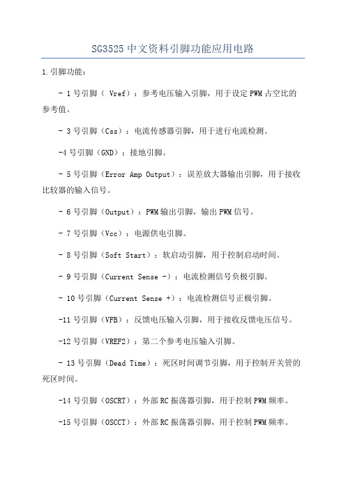
SG3525中文资料引脚功能应用电路1.引脚功能:- 1号引脚( Vref):参考电压输入引脚,用于设定PWM占空比的参考值。
- 3号引脚(Css):电流传感器引脚,用于进行电流检测。
-4号引脚(GND):接地引脚。
- 5号引脚(Error Amp Output):误差放大器输出引脚,用于接收比较器的输入信号。
- 6号引脚(Output):PWM输出引脚,输出PWM信号。
- 7号引脚(Vcc):电源供电引脚。
- 8号引脚(Soft Start):软启动引脚,用于控制启动时间。
- 9号引脚(Current Sense -):电流检测信号负极引脚。
- 10号引脚(Current Sense +):电流检测信号正极引脚。
-11号引脚(VFB):反馈电压输入引脚,用于接收反馈电压信号。
-12号引脚(VREF2):第二个参考电压输入引脚。
- 13号引脚(Dead Time):死区时间调节引脚,用于控制开关管的死区时间。
-14号引脚(OSCRT):外部RC振荡器引脚,用于控制PWM频率。
-15号引脚(OSCCT):外部RC振荡器引脚,用于控制PWM频率。
- 16号引脚(Vcc):电源供电引脚。
2.典型应用电路:2.1.单端输出开关电源2.2.双边输出开关电源2.3.应用于电动车充电器的开关电源总结:SG3525是一款功能强大的PWM控制芯片,拥有多个引脚用于输入电压、反馈电压、误差放大器输出等功能。
通过合理设计电路,可以应用于各种开关电源和逆变器的控制电路中,实现对输出电压和电流的精确调节和控制。
以上只是SG3525的一些典型应用,实际应用中还可以根据具体需求进行电路设计和优化。
IGBT FF300R17ME4中文数据手册中文数据资料
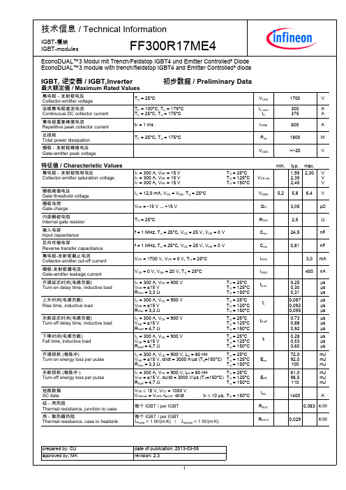
根据应用手册标定 Specificationaccordingtothevalidapplicationnote.
preparedby:CU approvedby:MK
dateofpublication:2013-03-05 revision:2.3 2
技术信息/TechnicalInformation
6,4 3,0 400
tr
td off
tf
IC = 300 A, VCE = 900 V, LS = 80 nH Tvj = 25°C VGE = ±15 V, di/dt = 3000 A/µs (Tvj=150°C) Tvj = 125°C RGon = 3,3 Ω Tvj = 150°C IC = 300 A, VCE = 900 V, LS = 80 nH Tvj = 25°C VGE = ±15 V, du/dt = 3000 V/µs (Tvj=150°C) Tvj = 125°C RGoff = 4,7 Ω Tvj = 150°C VGE ≤ 15 V, VCC = 1000 V VCEmax = VCES -LsCE ·di/dt 每个IGBT/perIGBT 每个IGBT/perIGBT λPaste=1W/(m·K)/λgrease=1W/(m·K) tP ≤ 10 µs, Tvj = 150°C
特征值/CharacteristicValues
正向电压 Forwardvoltage 反向恢复峰值电流 Peakreverserecoverycurrent 恢复电荷 Recoveredcharge 反向恢复损耗(每脉冲) Reverserecoveryenergy 结-壳热阻 Thermalresistance,junctiontocase 壳-散热器热阻 Thermalresistance,casetoheatsink
2SC3998中文资料(sanyo)中文数据手册「EasyDatasheet - 矽搜」
10 7
μs 5
3
2
SW时间 - IC
tstg
2SC3998
IC=5IB1 IB2= --2IB1 VCC=200V R称重
10
7
μs 5
3 2
SW时间 - IB2
tstg
VCC=200V IC=12A IB1=2.4A R称重
1.0 7
开关时间5 ,SW时间 -
3
tf
2
0.1 5
7 1.0
100
ICP=50A
5
基极电流IB2 - 一个
反向偏置一个S 0
100
5
3 2
10
5 3 2
集电极1.0电流,IC - 一个
5
3 2
7 10
2
ITR06231
IB2= --5A L=100μH
单脉冲
Tc=25°C
0.1
5
5 7 100
23
5 7 1000
集电极 - 发射极维持电压,VCEX(SUS) - V
PC - 锝
5
3 IC=25A
2
10
5 3 2
1.0
5
集电极3电流,IC - 一个
2
0.1
23
5 7 10
集电极电流,IC - 一个
正向偏置S 0
PC=250W
1m s
DCopera1tio0mns
23
5
ITR06230
300μs
5 3 2 0.01
3
4.0
5 7 10
2 3 5 7 100
集电极 - 发射极电压VCE - V
技术指标
绝对最大额定值
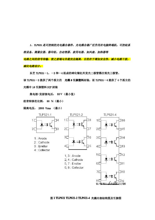
TLP521-4中文资料(光电耦合器 电流不大)
Rank GB 100
600
Blank, GR, BL, GB GR, BL, GB
*1: Ex. rank GB: TLP521−1 (GB)
(Note): Application type name for certification test, please use standard product type name,
2500vrms最小1tlp521tlp5212tlp52141tlp521tlp5212tlp5214图11ttllpp552211ttllpp55221122ttllpp55221144光藕内部结构图及引脚图2tlp52122tlp5212图22ttllpp55221122光电耦合器引脚排列图absolutemaximumratingsta25absolutemaximumratingsta25aabbssoolluutteemmaaxxiimmuummrraattiinnggss绝对最大额定值ttaa2255rating数值symbolunicharacteristic参数符号?t单位?tlp521??2??tlp521??1??tlp521??4forwardcurrent正向电流if7050ma????forwardcurrentif??093ta??05ta25maderating正向电流减率50ledpulseforwardcurrent瞬间ifp1100pulse100ppsa正向脉冲电流reversevoltage反向电压vr5vjunctiontemperature结温tj125??collector??emittervoltagevceo55v集电极发射极电压??emitter??collectorvoltageveco7v发射极集电极电压接收侧collectorcurrent集电极ic50ma电流collectorpowerdissipation1circuit集pc150100mw电极功耗collectorpowerdissipationcollectorpowerdissipationccoolllleeccttoorrppoowweerrddiissssiippaattiioonnderating1circuitta25pc?15?10mwderating1circuitta25pc?15?10mwddeerraattiinngg11cciirrccuuiittttaa2255ppcc??11
EEFUE0xxxxR中文资料

EE15
元器件交易网
Specialty Polymer Aluminum Electrolytic Capacitor
n
Standard Products
Rated W.V . (V.DC) 2 Case Size Specification Capacitance Ripple current (±20%) L W H ESR (A r.m.s./100kHz Ω (µF) (mm) (mm) (mm) +20 to +105 °C ) 330 150 150 180 180 220 220 270 120 120 150 150 180 100 100 120 120 150 68 100 270 270 330 330 390 390 470 470 220 220 270 270 330 330 390 180 180 220 220 270 150 150 180 180 220 100 150 7.3 7.3 7.3 7.3 7.3 7.3 7.3 7.3 7.3 7.3 7.3 7.3 7.3 7.3 7.3 7.3 7.3 7.3 7.3 7.3 7.3 7.3 7.3 7.3 7.3 7.3 7.3 7.3 7.3 7.3 7.3 7.3 7.3 7.3 7.3 7.3 7.3 7.3 7.3 7.3 7.3 7.3 7.3 7.3 7.3 7.3 7.3 4.3 4.3 4.3 4.3 4.3 4.3 4.3 4.3 4.3 4.3 4.3 4.3 4.3 4.3 4.3 4.3 4.3 4.3 4.3 4.3 4.3 4.3 4.3 4.3 4.3 4.3 4.3 4.3 4.3 4.3 4.3 4.3 4.3 4.3 4.3 4.3 4.3 4.3 4.3 4.3 4.3 4.3 4.3 4.3 4.3 4.3 4.3 2.8 2.8 2.8 2.8 2.8 2.8 2.8 2.8 2.8 2.8 2.8 2.8 2.8 2.8 2.8 2.8 2.8 2.8 2.8 2.8 4.2 4.2 4.2 4.2 4.2 4.2 4.2 4.2 4.2 4.2 4.2 4.2 4.2 4.2 4.2 4.2 4.2 4.2 4.2 4.2 4.2 4.2 4.2 4.2 4.2 4.2 4.2 3.3 3.0 3.3 3.0 3.3 3.0 3.3 3.0 3.0 3.3 3.0 3.3 2.5 3.0 3.3 3.0 3.3 2.5 3.0 2.5 3.3 3.5 3.3 3.5 3.3 3.5 3.3 3.5 3.3 3.5 3.3 3.5 3.3 3.5 3.3 3.3 3.5 3.3 3.5 3.0 3.3 3.5 3.3 3.5 3.0 3.3 3.0 Part number
电子器件中文资料

下边资料的次序是纳米盘上的自动排列,请需要者自己看着找吧。
最后还有07年全年的《读者》E书下载,及几个小游戏。
4000系列数字集成电路资料大全.4000.rar/d/7d8425c10a0ff161c3e0e00037737a69c5d3980411432404AD620中文资料.pdf/d/b1961b23b272d8531b9f390fa570ae2c71c2d45024a6050074系列数字集成电路手册大全.pdf/d/b4c283d67d1af4aacf7b7c19d3d5aa3b71a8c58d7692c801速查速用世界可控硅代换手册.pdf/d/be70c47f9fc76db61c62e1caf90d0f4a87d1a68459699901最新集成电路应用300例.rar/d/365971ce99cae66629dd2d76d45b0307e83a21d461b83900怎样使用运算放大器.pdf/d/8ca6ba96b0a2d9d8ed0023ecde54908c909fb5cc8c8e2900新型实用电路制作200例.rar/d/b9f585eb5512f27c380fc3e01ce465e105592c00548f7d00新型电子电路应用实例精选.rar/d/2cd40d687adff1a0031927956c3ae4b16bd41b6489d48e00电子线路设计应用手册.rar/d/86601a2c9c3d346da2b7582806c525fc91e3cf55109a6301新编电子电路大全.rar/d/0ed4b1cba5ad94a5bdfabd410aae1c058c2bbd65aa8f6e00电子电路及电子器件.rar/d/0856a0265ffdc5947a7a4fe93ea34fa53539165b851ea700数字电路.rar/d/00fca0f91805c0f137bcfdc966caba0297c0e6d7dd4c3b00实用双向可控硅应用500例.rar/d/3ebb740d73718fb3cda67b20cb2d50620430f264cc2d6a00实用电子线路集.rar/d/4873ecc0445c91c3d7b444d6b71056bd6b45dc89ef6b8100实用电子电路大全.rar/d/2ca46fb365cedaee9451b79c697e8ff474d22aa6c5ebaf00实用单元电路及其应用.rar/d/3c77fff6e45fddf87dee1bf7788a1c242b1d1c4ef9119600三极管资料大全.rar/d/00de8710ba6c1e8c289ecaf61208d6b6ea32504677a90000绝对精品的硬件设计方面资料.rar/d/c8d1606af74af0a6f7a7f414376c7137e200fb588e460600简易可控硅整流电源电路.pdf/d/28430231e150b19c1d91d1a52f0104a8fef4b07eee510000电子电路大全(合订本).rar/d/7c041e86b457278bc289756622eca10562b31d68f6ba7a01电子电路集.pdf/d/cc133c04fb2ebe2abc1ed4b2a363046e6bff0d2bf8c04100电子电路百科全书(第五卷).rar/d/18148ed5200f99e6176c888024eb8e72d323fcf3e2007900电子电路.pdf/d/f1836309214f28fd8227efa0969e0d39c5261f29c88d4400电子爱好者实用电子制作.rar/d/05edad0c1b9b9c98eabc2847ca8a5d4cfa4fea48d9331f00常用电子元气件手册.pdf/d/f42c221af44585fee096c2b2c3f5d5da87591f3a7a143600常用电子元器件图片.pdf/d/90f6611e31ac9f60a761abb7af0ba31f50fb5a2a781f1c00常用稳压芯片篇.txt/d/6224bdf4fe9e168d36f3ef223422b6add262a8ed810c0000常用电子元器件简明手册.rar/d/00b9d1eedddd798047798152c65d916e257ff4e277702300常用电子元气件命名.pdf/d/3c89dc7fbb8fd14f64b93d946f16583a5c0c3848ce720800P8xC591_cn.pdf/d/8e6c43250690dc6baee98e3865798ee4fc85f5724ba14d00MAX485中文资料.pdf/d/15b701ca1ffd126726fdf070ea1f018d8344aa8bf19c0d00MAX280中文资料.pdf/d/12a35473a7bb0afbb25d41f079b2cbd5af770460877b0100MAX194中文资料.pdf/d/c4a65303e4422f2b661ee713c44e3000ab1ec8baf34b0100T8变压器.pdf/d/86d97d9ca03ec16cb94e885a63912561864f0dfb384d0200NE555.pdf/d/6eeb2db556192e988d3f45d6fc6a976d3743a54695d40300LM7805中文资料.pdf/d/20ade1675d2aebb22a5b7e8596cf421ad74fb6e0bc680400NE555中文资料.pdf/d/4437cbafdb450d9803022a7f145806736178b2647d8e0000MC1413.pdf/d/a8b41856cce7d8c13e68d7be0f7eba717d00bcc2be460100MCP3202中文资料.pdf/d/e6652d4504073a352f4a6e628575bcb68cd4b7bac3ed0b00MC3423.PDF/d/1856c527d115fecf23c7cc792b2df521f434795f4ad80100LM358中文资料.pdf/d/01055a8e69fd7f39469037ab678f9ed4a2807672378c0100LM339.rar/d/8c8b06f70cccad70c338f9f8bb9bf85745f5340af9480000lm2596.pdf/d/67de0105031f80ad657a9558635c3a8b38140cc53ada0c00LM2576中文资料.pdf/d/fc5567b2fa37f7ce88b5272536b2d817eb231c50971e0400lm1117中文资料.pdf/d/f24586db9afc12e7f9bf32371f24b389452a1cc4a7bb0b00LM393中文资料.pdf/d/1961b1559934b7bf617ae57027e87ebb7d12aea50a9a0300LM363中文资料.pdf/d/7e83da8b44365c274829b181ecf725a2291407804cb40100LM7909中文资料.pdf/d/8ce4617cb1123fda1ad10ad38d4493a6480e86f5d4bf0000LMD18200.doc/d/a7e301b93175eb71345299272395fce9e06a30a8009c0100lm324中文资料.pdf/d/cc590a103a433200fdfb3a57f44f5f383d2ee0b4557d0a00LM317中文资料.pdf/d/686a9606b1dd1cca239d8a6bcc8e27d4b45c1f8c24d50d00lm211lm311中文资料.pdf/d/eb9f6ebac497c099445f95a4ad95a0a44730341a715d0b00LM140.pdf/d/3876aea02373e492cdb7da633c9ba26d5f250e06d8e10200LM358.pdf/d/7816ffab592a9e37d9c493dd238fc6b6e55397be8e5e0100LM109.pdf/d/a70eaf6138bb71be74d0431224cbd5d0c7f1136a55740100lm3s317_ds_cn.pdf/d/bd34bf2a2ab69f935911e60206bd5e1a67e6f06ca0215d00 LF398中文资料.pdf/d/bcd8edd55f76babe047e7e1e8e61045af8129ab1866e0100L290-L291-L292.pdf/d/2e0ab9638f84016c18a6ff0fc817b8dbf1043857e30b0400ICL7135中文资料.pdf/d/71e1b23dbc5dff6f6fef9c002be6420f5968745750710800ICL7104中文资料.pdf/d/e07abec1e557ad53c159d7156237bfa86e842cb549820100fm3135_ds.pdf/d/fc97032bc0142c568bdd39f8140d82c6ae4ee9b175260400cd40161中文资料pdf.pdf/d/40230b71ccbbc78b9355e8946d1e4391efecf2199da10200最新世界三极管特性代换手册.r/d/6605148cde3dddb2a4bb9123eb0dcdb6721a053f286c7601lm3s310_ds_cn.pdf/d/bb01eb82cbddbc6fabae95b5a3f631f1d32d3331750e5700cmos4000器件中文资料.pdf/d/bde8cef1903e5f776ddae591fe4b9fe4dd41fa2023074800cd40109中文资料pdf.pdf/d/202883c137a9443ae5aad82ac01c0c5d5b027bfceeb50100cd40105中文资料pdf.pdf/d/b56e06f4a9b172b10908429505b829f1b06b46934bca0100ds1302中文资料.pdf/d/8ffe86b97d76a8cc3fffe2b8b7d7d411ea84ad0bac730300cd40163中文资料pdf.pdf/d/305f9eca8225b8333aafa3a1bd0c4c3c1c3ac34338a10200cd40147中文资料pdf.pdf/d/e3380153eb1198bc857e579999fc3dddb55b460294f20100cd4076中文资料.pdf/d/d000f62e7c0c80c37332f73d5a9200afa8a7f4b572f30200cd4071中文资料.pdf/d/49f8cce83e6ab3e4d593fa45e1f0e685dcbb5186db3a0200cd4070中文资料.pdf/d/82edf36cc8617e3356612ac573e356ba89959470a3420200cd4068中文资料.pdf/d/18c87ad5f8690c9cd1a33121bfd1ba3040256c7d8f490200cd4067中文资料.pdf/d/e6966eea3a191a3186dd7bfb5f19f031b430ea7121530200cd4055中文资料.pdf/d/33d92d1285e92130dbb263df34bebe04f1418d98e29f0300cd4038中文资料.pdf/d/bebc590afbebe766436886d23fbc5205344cbe07d5690300cd4029中文资料pdf.pdf/d/0d4dc7d75ded5885fd3e475e8071f438921d796cbd750400cd4048中文资料.pdf/d/846d38f344ce9ef88598d6e69a542300fed3c3d7d33f0200cd4047中文资料.pdf/d/36a5eec356ffc0baf497d07e71f28081732d28bc145e0200cd4035中文资料.pdf/d/c7b4075b5bda2910cbfdc61bd13730a2d7ab41f161a10300cd4034中文资料.pdf/d/b6dadf2ee2883540208c0f0e06d930fbbf0812016faf0400cd4028中文资料pdf.pdf/d/557cd672fe94a58e1e0c7b508bd095c74c7851d7fb820300cd4024中文资料pdf.pdf/d/c2196481f081938dbb92ed67395098e681fac3206cf10300cd4027中文资料pdf.pdf/d/348e802290198d2503df1013653fd744b97ccdba31ef0200 AT89S51.pdf/d/dccdecb6e6192d5581e790a27bf787eb9a354e1335350900cd4053.pdf/d/404342f322a3a932c98775f207d3ebfd4086551dacb10200cd4034中文资料.pdf/d/49106b6ade07c448f2e9f0d4c232dd8f818961bf6faf0400cd4028中文资料pdf.pdf/d/21e60f5ad93242cad1720458dce6b23333765ec7fb820300cd4027中文资料pdf.pdf/d/60d154cb4a834783bdc59afd3385cd025*********ef0200cd4022中文资料pdf.pdf/d/1057c76c8deff8300c6a6db430ba3282d53d9dbfc70d0400att7021cn.pdf/d/0e5d65285c35682e713bddf0a405e0326a64aba2c6c20a00BA5101BA5201.pdf/d/5d16c3c4e4ac5e156c4241ea590dba00ef7246403acf0400AT89S51.pdf/d/237f01593ba5bddc8665e29116ff139e19c340d435350900AT89LV52.pdf/d/5879e4ac095f60ca5e2b92beb242eaac1c5665cedf300800ad9850中文资料.pdf/d/38a283d55c2c6ceb04694c7a5534c3ae16ab96a6dc6e1c00AT89C1051U.pdf/d/559f6cf5bc2aefa3bbaf4bc6d6f9dd17042dcba1f8d40400 AD673.pdf/d/559f6cf5bc2aefa3bbaf4bc6d6f9dd17042dcba1f8d40400AD620中文资料.pdf/d/145656a8efc258c014c5330ed03482a33a04ea6524a60500AD594_595.pdf/d/6028f9ccfdf02af289e312c94ef8cfc0d9275efdb6220200AD346中文资料.pdf/d/7bd0a4417a8213a7dc982986fbcdae8ce53d9e53fa4401009013.pdf/d/9057c57766e0d1fded4e6a49804e23949c2177bc6d9501008050.pdf/d/24e3b9655ebf0b2f019abd07baaa995fa98f45bf31a1020078xx.pdf/d/af10e44a0a8b804bdd6336b88e2188cf195375644b1c010074LS164中文资料.pdf/d/201383c7b23d7057d102cfc148946d045797b4a88914030074ls245中文资料.pdf/d/37f26e3d5349c02dc216bdc7a487060d1332e94f7501030074LS138中文资料.pdf/d/52f4c8c7b39181704008ceb6e89ea8095faaab98cbbe030074ls138.PDF/d/7aa7e214ce5dfe4c5dce8d9c78ab396289ca517377b9030074ls74.PDF/d/9e1051ab95e509fe3414830be349e6d7d6f56374297a060074ls04.PDF/d/e8a4bad83b00a61a514f295ef7d36aa064801b744472040074LS14中文资料.pdf/d/8938dbc43cdb1a232112a8f69e0b0f7e50357cb54389030074HC245中文资料.pdf/d/d045498e1b5a8b831fb554e3059f7c9c6a3ed92d1701030024c02中文官方资料手册pdf.pdf/d/5463179db3bbb8a494d38f0ab48c8cbb9cf6aece299c090074ALS245.pdf/d/b4c462102ac87887e8e5059e001f16647c213459b13f01004N25中文资料.pdf/d/c818ecf73638d05fb5489690e28b91c94c0976af7ccb0100USB DISK EJECT.EXE/d/4102ee837c5b11d7d7e3d40c759bd5b384154f33007c0d00TEA1062.pdf/d/569c7b2bf61ebf2e2c01d7fcb3bdb0a3f1b83a0d8b4e030078xx.pdf/d/dc3547b7951a28c30c447002adfc743b2cd8174a4b1c010074ls245中文资料.pdf/d/f0fd2d9a704cfc09571d7f694b8e5625ea2577f57501030074LS138中文资料.pdf/d/8df689b9e0e1157387ae34ffb186587654607dc5cbbe030074ls138.PDF/d/906f5068200722722dd009f2c0558d2ca954855d77b9030074ls74.PDF/d/d4ce35981359c38e4e10a143913dbc77ec41b17c297a060074LS14中文资料.pdf/d/500d0dd2c24ca57fdd5f81887ce014ee383cf15f4389030074ls04.PDF/d/00b330534fc4824625e3f5aadb970e2cb07c17204472040024c02中文官方资料手册pdf.pdf/d/0dfded751578a730e85acec4fecb3ff3ecb3e344299c090074HC245中文资料.pdf/d/ff5c91227f1bf663c1326fc19d5295f02035768b1701030074ALS245.pdf/d/0347de88ba42c7981ec9d8cb0829ed27dee125a8b13f01001N4148smd.pdf/d/885391bb8724b237c52840be7996214047193380cfa008002n4403.PDF/d/20bc155264d25b57a981c63afab4b0be6bb806f2b4f700002n4401.PDF/d/40c749e3a06284cca55f4964a1322308e344b26651f70000LMD18200.doc/d/58c3a544b3cc4481889d5c85b54087756849a92e009c0100。
31402-3110资料

FEATURES AND SPECIFICATIONSSPECIFICATIONSAPPLICATIONS2.54mm (.100”) Pitch MX64 Single Row Sealed Connectors 31402, 31403, 31404Small and compact, the MX64 single row female connectors set the standard for 2.54mm (.100”) pitch sealed connectors. Available sizes include the 1-by-2, 1-by-3, 1-by-4, 1-by-5, 1-by-6 and 1-by-8. These connectors also allow for the greatest level of flexibility by accommodating three different female terminal systems. These include the GET female terminal (Series 34230), commonly used at Ford Motor Company, the Kaizen female terminal, commonly used at General Motors and the MX64 female terminals (Series 33467 and 33468), commonly used at Daimlier Chrysler and the general market. In addition, by working with USCAR to optimize the overall size of these connectors, Molex tooled the 1-by-4, 1-by-5, 1-by-6 and 1-by-8 parts to the USCAR-defined Z02 footprint resulting in up to a 25% size reduction in the mating interfaces.For additional information on USCAR footprints and performance specifications, visit the USCAR website at .Reference InformationPackaging: BulkMates With: Sensors, other USCAR interfaces Designed In: MillimetersRecommended Automotive Applications:31402 (Ford Motor)31403 (Daimler Chrysler/General Market)31404 (General Motors)ElectricalVoltage: 250VCurrent: 0.64mm (.025”) Terminals – 7.0 to 10.0A (depending on manufacturer of female terminals)Dielectric Withstanding Voltage: DC500V Resistance: 100 M ȑmin.Isolation: 20 M ȑmin.MechanicalInsertion Force: Less than 75N (16.9 lb) per connector Unmate Efforts: Less than 75N (16.9 lb) per connector Connector Lock Strength: 110N (24.7 lb) min.Female Terminal Retention: Greater than 75N (16.9) with the TPA engagedPhysicalTerminal Pitch:Horizontal 2.54mm (.100”); Vertical 2.54mm (.100”)Housing: PBT + 30% Glass Filled Female Terminals:For 31402 Series use 34230 GET, Tin Plated For 31403 Series use 33467 MX64, Gold Platedor 33468 MX64, Tin platedFor 31404 Series, terminals are manufactured by Yazaki Operating Temperature:USCAR Class III -40 to +125°CFeatures and BenefitsI Meets all USCAR footprints and testing requirements for 0.64mm (.025”) pitch square pin connector systems in compliance with OEM directivesI Ability to accommodate Ford, GM or DCX approved female terminals provides design flexibilityI Matte seal design eliminates secondary operation and costs associated with cable seals I Available with or without CPA for added locking protection when CPA is usedI Accommodates 18-22 AWG wire and metric wires to support US or offshore wire requirementsI Circuit sizes 1-by-4,1-by-5,1-by-6 and 1-by-8 meet the USCAR Z02 optimized footprints and are up to 25%smaller in size as compared to the Z01 footprintsI Four polarization options available protect against mis-matingI Special polarization color (black) in B,C,D configurations is available for use when earth-toned connectors (black,brown and gray) are used in high visibility packaging areaMX64 Single Row Female Connectors Are Designed to USCAR-Approved Footprints and Meet USCAR Testing RequirementsI Automotive - Sensors I Commercial - SensorsColor CodedPolarization Options31402, 31403, 3140431402, 31403, 3140431402, 31403, 31404Americas Headquarters Lisle, Illinois 60532 U.S.A.1-800-78MOLEX amerinfo@ Far East North Headquarters Yamato, Kanagawa, Japan 81-462-65-2324feninfo@ Far East South Headquarters Jurong, Singapore 65-6-268-6868fesinfo@ European Headquarters Munich, Germany 49-89-413092-0eurinfo@Corporate Headquarters 2222 Wellington Ct.Lisle, IL 60532 U.S.A.630-969-4550Fax:630-969-1352Visit our Web site at /auto/mx64.htmlOrder No. USA-274Printed in USA/JI/2004.11©2004, Molex。
- 1、下载文档前请自行甄别文档内容的完整性,平台不提供额外的编辑、内容补充、找答案等附加服务。
- 2、"仅部分预览"的文档,不可在线预览部分如存在完整性等问题,可反馈申请退款(可完整预览的文档不适用该条件!)。
- 3、如文档侵犯您的权益,请联系客服反馈,我们会尽快为您处理(人工客服工作时间:9:00-18:30)。
Broadband TelCom Power, Inc. BTCPower TM Redefining “Current” Limits In Power Conversion BTCPower
4EE Series 25-30W DC-DC Converters Features
• 25W Isolation output
• 4:1 Input Range
• Six-sided Shield
• Remote On/Off Control
• Efficiency To 82%
• 200KHz switching frequency
Model Input Output Output Input Current % Efficiency Case Number Voltage Voltage Current No Load Full Load
4EE-01 5 VDC 3000 mA15 mA 810 mA 77
4EE-02 12 VDC 1250 mA15 mA 780 mA 80
4EE-03 15 VDC 1000 mA15 mA 780 mA 80
4EE-04 9-36 VDC ±12 VDC±625mA20 mA 780 mA 80 E 4EE-05 ±15 VDC±500mA20 mA 780 mA 80
4EE-06 5/±12 VDC 1500/±310 mA20 mA 780 mA80
4EE-07 5/±15 VDC 1500/±250 mA20 mA 780 mA80
4EE-08 +5/+12/-5 VDC 1500/310/500 mA20 mA 715 mA80
4EE-11 5 VDC 3000 mA10 mA 410 mA77
4EE-12 12 VDC 1250 mA10 mA 390 mA80
4EE-13 15 VDC 1000 mA10 mA 390 mA80
4EE-14 18-72 VDC ±12 VDC±625mA15 mA 380 mA82 E 4EE-15 ±15 VDC±500mA15 mA 380 mA82
4EE-16 5/±12 VDC 1500/±310 mA15 mA 380 mA82
4EE-17 5/±15 VDC 1500/±250 mA15 mA 380 mA82
4EE-18 +5/+12/-5 VDC 1500/310/500 mA15 mA 350 mA82
Note: Nominal Input Voltage 12, 24, 28 or 48VDC
Broadband TelCom Power, Inc. –1719 S. Grand Avenue, Santa Ana, CA 92705 U.S.A. Tel.: 714-259-4888 • Fax: 714-259-0840• • Email: sales@ DS LP 4EE Rev2 16-1-04
4EE Series 25-30W DC-DC Converters
BTCPower BTCPower
T M
Broadband TelCom Power, Inc. – 1719 S. Grand Avenue, Santa Ana, CA 92705 U.S.A.
Tel.: 714-259-4888 • Fax: 714-259-0840• • Email: sales@ DS LP 4EE Rev2 16-1-04
Specifications
Input Specifications:
Input Voltage Range…………….……24V……...………………..9-36V 48V……………………..18-72V Input Filter…………………………………………………..……..Pi Type Output Specifications: Voltage Accuracy
Single output………………………..…………………….+/- 1.0 % max. Daul output………………………………………………..+/- 3.0 % max. Triple, 5V………………………………………………….+/- 2.0 % max. 12V/15V…………………………………………..………+/- 3.0 % max. Voltage Balance ( Dual )………………………………...+/- 1.0 % max. External trim Adj. Range……………………………..…………+/- 10% Ripple & Noise, 20 MHz BW……………………….… 75 mV p-p max. Temperature Coeffcient………………………… +/- 0.02 % / ºC max. Short Circuit Protection………………………………..……Continuous Line Regulation ¹ Single / Dual Output………….……..+/- 0.2 % max. Triple………………………….………..+/- 1.0% max. Load Regulation ² Single / Dual Output…………….….+/- 1.0 % max. Triple………………………..…………+/- 5.0 % max. General Specifications :
Efficiency………………………………………………..……..see table Isolation Resistance…………………………………………..100Mohm Switching Frequency……………………………………..200 KHz, min. Operating Temperature Range…………………………-25ºC ~ +71ºC
Case Temperature………………………………………….100 ºC max. Cooling……………………………………………….Free air convection Storage Temperature Range……………………..…..-55 ºC ~ +105ºC Isolation Voltage………………………….………………..500VDC min. EMI/RFI…………………………………….....Six-sided continus shield Dimensions…………………2.65” x3” x 0.83 “(65 x 76.2 x 21.1 mm) Case Material……..Black Coated Copper with Non-conducted base
Triple output loading table
Ouput Voltage Amperes (pin no.)
(V) Min. (2) Nom. 6 +5 0.25 1.5 3 & 5 +12 or -12 0.1 0.31 3 & 5 +15 or -15 0.1 0.25 3 & 5
+12 or -5
0.1/0.1 0.31/0.5
Note: 1. measured from high lin to low line
2. measured from full load to ¼ load
3. maximum total power from all outputs is limited to 25/30W but no output should be allowed to exceed its maximum current
4. minmum current on each output is required to maintain specified regulation
Outline Information and Pin-out
Pin Connection
Pin Single Dual Triple 1 +Input +Input +Input 2 -Input -Input -Input 3 No pin +Output
+Output 4 Trim Common Common 5 No pin -Output -Output 6 +Output No pin +5V output 7 -Output
No pin No pin 8 Remote On/Off Control
Remote On/Off Control
Logic compatibility CMOS or Open collector TTL E c-0n >5.5 Vdc or open circuit E c-Off <1.8 Vdc Shutdown Idle current 10mA Input resistance 100K ohms (Ein 0Vdc to 9Vdc) Control common referenced to Input minus External Output Trimming
Output may optionally be externally trimmed (+/-10%) with a fixed resistor or an external trimpot as shown.。