C0940中文资料
CD4029中文资料

5.0 10.0 15.0 5.0 10.0 15.0 5.0 10.0 15.0 5.0 10.0 15.0
5.0 10.0 15.0
规范值
最小
最大
500
240
180
560
260
190
200
100
80
200
100
80
2.0
-
4.0
5.5
-
180
90
60
-
15
15
15
60
20
12
340
140
100
动态特性(TA=25℃): 参数
测试条件
CP 操作
tPLH、tPHL 传输 延迟时间
CP → Q
CP → CO
CL=50pF RL=200k tr=20ns tf=20ns
tTLH、tTHL 输出 转换时间
CP → Q
CP → CO
fcp
CP 频率(对 CO)
tw
CP 脉冲宽度
tr、tf
CP 上升或下降时 间
电子工程师之家
CC4029------4位二进制/十进制加减计数器 简要说明:
CC4029 是由具有预进位功能的 4 位二进制或 BCD 码十进制加减计数器构成。 LD 为高电平时,D0~D3 预置计数器为任何状态,为低电平时,对计数器清零。当 CI 和 LD 均为低电平时,在时钟上升沿计数器计数。CO 一般为高电平,只有在加至最 大或减至最小时,为低电平。计数器闲置时, CI 端需与 Vss 相连,当 B/ D 为高电 平时,以二进制计数;反之,为十进制。U/ D 为高电平时,为加计数器;反之,为 减计数器。
FPGA可编程逻辑器件芯片EP4CE40F29I7N中文规格书

Chapter 5:Clock Networks and PLLs in Arria II DevicesPLLs in Arria II Devices Arria II Device Handbook Volume 1: Device Interfaces and IntegrationBypassing PLLBypassing a PLL counter results in a multiply (m counter) or a divide (n and C0 to C9 counters) factor of one.Table 5–20 lists the settings for bypassing the counters in Arria II PLLs.f For more information about how to use the PLL scan chain bit settings, refer to thePhase Locked-Loops Reconfiguration (ALTPLL_RECONFIG) Megafunction User Guide .1To bypass any of the PLL counters, set the bypass bit to 1, causing the values on theother bits to be ignored. To bypass the VCO post-scale counter (K ), set thecorresponding bit to 0.Dynamic Phase-ShiftingThe dynamic phase-shifting feature allows the output phases of individual PLLoutputs to be dynamically adjusted relative to each other and to the reference clock without having to send serial data through the scan chain of the corresponding PLL. This feature simplifies the interface and allows you to quickly adjust clock-to-out (t CO ) delays by changing the output clock phase-shift in real time. This adjustment isachieved by incrementing or decrementing the VCO phase-tap selection to a given C counter or to the M counter. The phase is shifted by 1/8 of the VCO frequency at a time. The output clocks are active during this phase-reconfiguration process.Table 5–21 lists the control signals that are used for dynamic phase-shifting.Table 5–20.PLL Counter Settings for Arria II Devices PLL Scan Chain Bits [0..8] SettingsLSBMSB Description 0(1), X (2)X X X X X X X 1 (3)PLL counter bypassed X X X X X X X X 0 (3)PLL counter not bypassed because bit 8 (MSB ) is set to 0Notes to Table 5–20:(1)For Arria II GX devices.(2)For Arria II GZ devices(3)Counter-bypass bit.Table 5–21.Dynamic Phase-Shifting Control Signals for Arria II Devices (Part 1 of 2)Signal Name DescriptionSource Destination PHASECOUNTERSELECT[3:0]Counter select. Four bits decoded to selecteither the M or one of the C counters for phaseadjustment. One address maps to select allC counters. This signal is registered in the PLLon the rising edge of scanclk .Logic array or I/O pins PLL reconfiguration circuit PHASEUPDOWN Selects dynamic phase shift direction;1=UP;0=DOWN. Signal is registered in thePLL on the rising edge of scanclk .Logic array or I/O pin PLL reconfiguration circuit PHASESTEPLogic high enables dynamic phase shifting.Logic array or I/O pin PLL reconfigurationcircuitChapter 6:I/O Features in Arria II DevicesI/O StructureI/O registers are composed of the input path for handling data from the pin to thecore, the output path for handling data from the core to the pin, and the output enablepath for handling the OE signal to the output buffer. These registers allow fastersource-synchronous register-to-register transfers and resynchronization. You canbypass each block of the output and output enable paths. Figure6–3 and Figure6–4show the Arria II IOE structure.Figure6–3.IOE Structure for Arria II GX DevicesArria II Device Handbook Volume 1: Device Interfaces and IntegrationChapter 2:Logic Array Blocks and Adaptive Logic Modules in Arria II DevicesLogic Array Blocks Arria II Device Handbook Volume 1: Device Interfaces and Integration The LAB of the Arria II device has a derivative called memory LAB (MLAB), which adds look-up table (LUT)-based SRAM capability to the LAB. The MLAB supports a maximum of 640bits of simple dual-port SRAM. You can configure each ALM in an MLAB as either a 64 × 1 or 32 × 2 block, resulting in a configuration of 64 × 10 or32 × 20 simple dual-port SRAM blocks. MLAB and LAB blocks always coexist as pairs in Arria II devices. MLAB is a superset of the LAB and includes all LAB features.Figure 2–2 shows an overview of LAB and MLAB topology.f For more information about MLABs, refer to the TriMatrix Memory Blocks in Arria IIDevices chapter.Figure 2–B and MLAB Structure in Arria II DevicesNote to Figure 2–2:(1)You can use an MLAB ALM as a regular LAB ALM or configure it as a dual-port SRAM.MLABLAB。
EP3C25Q240C8中文资料(Altera)中文数据手册「EasyDatasheet - 矽搜」

—
1.71 1.8 1.89
V
—
1.425 1.5 1.575 V
电源电压为输出缓冲器,1.2-V
手术
—
1.14 1.2 1.26
V
VCCA (3)
VCCD_PLL (3) VI VO
供应(模拟)电压PLL
调节器
供应(数字)电压PLL
输入电压 输出电压
TJ
工作结温
tRAMP IDiode
电源斜坡时间
电源电压为输出缓冲器,3.3-V
手术
—
1.15 1.2 1.25
V
—
3.135 3.3 3.465 V
电源电压为输出缓冲器,3.0-V
手术
—
2.85
3
3.15
V
VCCIO (3), (4)
电源电压为输出缓冲器,2.5-V
手术
电源电压为输出缓冲器,1.8-V
手术
电源电压为输出缓冲器,1.5-V
手术
—
2.375 2.5 2.625 V
直流电流幅度
当启用PCI-钳位二极管
—
— — —
对于商业用途 工业用 对于扩展温度 对于汽车使用 标准上电复位
(POR) (5) 快速POR (6)
—
2.375 2.5 2.625 V
1.15 1.2 1.25
V
–0.5 —
3.6
V
0
—
VCCIO
V
0
—
85
°C
–40 — 100 °C
–40 — 125 °C
表1-4 列出I / O引脚泄漏 目前Cyclone III器件.
f
有关功耗估算工具更多信息 ,请参
CD4019中文资料
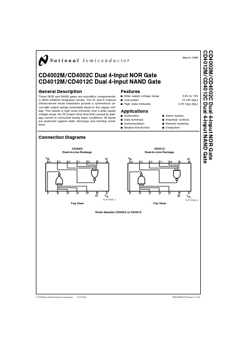
TL F 5940CD4002M CD4002C Dual 4-Input NOR Gate CD4012M CD4012C Dual 4-Input NAND GateMarch 1988CD4002M CD4002C Dual 4-Input NOR Gate CD4012M CD4012C Dual 4-Input NAND GateGeneral DescriptionThese NOR and NAND gates are monolithic complementa-ry MOS (CMOS)integrated circuits The N-and P-channel enhancement mode transistors provide a symmetrical cir-cuit with output swings essentially equal to the supply volt-age This results in high noise immunity over a wide supply voltage range No DC power other than that caused by leak-age current is consumed during static conditions All inputs are protected against static discharge and latching condi-tionsFeaturesY Wide supply voltage range 3 0V to 15V Y Low power10nW (typ )YHigh noise immunity0 45V DD (typ )ApplicationsY Automotive Y Alarm system Y Data terminals Y Industrial controls Y Instrumentation Y Remote metering YMedical ElectronicsYComputersConnection DiagramsCD4002Dual-In-Line PackageTL F 5940–1Top ViewCD4012Dual-In-Line PackageTL F 5940–2Top ViewOrder Number CD4002or CD4012C 1995National Semiconductor Corporation RRD-B30M105 Printed in U S AAbsolute Maximum Ratings(Note1)If Military Aerospace specified devices are required please contact the National Semiconductor Sales Office Distributors for availability and specifications Voltage at Any Pin V SS b0 3V to V DD a0 3V Operating Temperature RangeCD4002M CD4012M b55 C to a125 C CD4002C CD4012C b40 C to a85 C Storage Temperature Range(T S)b65 C to a150 C Power Dissipation(P D)Dual-In-Line700mW Small Outline500mW Operating Range(V DD)V SS a3 0V to V SS a15V Lead Temperature(T L)(Soldering 10seconds)260 CDC Electrical Characteristics CD4002M CD4012MLimitsSymbol Parameter Conditions b55 C a25 C a125 C UnitsMin Max Min Typ Max Min MaxI DD Quiescent V DD e5 0V0 050 0010 053 0m ADevice Current V DD e10V0 10 0010 16m A P D Quiescent Device V DD e5 0V0 250 0050 2515m W Dissipation Package V DD e10V1 00 011 060m W V OL Output Voltage V DD e5 0V V I e V DD I O e0A0 0500 050 05V Low Level V DD e10V V I e V DD I O e0A0 0500 050 05V V OH Output Voltage V DD e5 0V V I e V SS I O e0A4 954 955 04 95V High Level V DD e10V V I e V SS I O e0A9 959 95109 95V V NL Noise Immunity V DD e5 0V V O e3 6V I O e0A1 51 52 251 4V (All Inputs)V DD e10V V O e7 2V I O e0A3 03 04 52 9V V NH Noise Immunity V DD e5 0V V O e0 95V I O e0A1 41 52 251 5V (All Inputs)V DD e10V V O e2 9V I O e0A2 93 04 53 0V I D N Output Drive Current V DD e5 0V V O e0 4V V I e V DD0 50 401 00 28mAN-Channel(4002)V DD e10V V O e0 5V V I e V DD1 10 92 50 65mA (Note2)I D P Output Drive Current V DD e5 0V V O e2 5V V I e V SS b0 62b0 5b2 0b0 35mAP-Channel(4002)V DD e10V V O e9 5V V I e V SS b0 62b0 5b1 0b0 35mA (Note2)I D N Output Drive Current V DD e5 0V V O e0 4V V I e V DD0 310 250 50 175mAN-Channel(4012)V DD e10V V O e0 5V V I e V DD0 630 50 60 35mA (Note2)I D P Output Drive Current V DD e5 0V V O e2 5V V I e V SS b0 31b0 25b0 5b0 175mAP-Channel(4012)V DD e10V V O e9 5V V I e V SS b0 75b0 6b1 2b0 4mA (Note2)I I Input Current10pANote1 ‘‘Absolute Maximum Ratings’’are those values beyond which the safety of the device cannot be guaranteed Except for‘‘Operating Temperature Range’’they are not meant to imply that the devices should be operated at these limits The table of‘‘Electrical Characteristics’’provides conditions for actual device operationNote2 I D N and I D P are tested one output at a time2DC Electrical Characteristics CD4002C CD4012CLimitsSymbol Parameter Conditions b55 C a25 C a85 C UnitsMin Max Min Typ Max Min MaxI DD Quiescent V DD e5 0V0 50 0050 515m ADevice Current V DD e10V5 00 0055 030m A P D Quiescent Device V DD e5 0V2 50 0252 575m W Dissipation Package V DD e10V500 0550300m W V OL Output Voltage V DD e5 0V V I e V DD I O e0A0 0500 050 05V Low Level V DD e10V V I e V DD I O e0A0 0500 050 05V V OH Output Voltage V DD e5 0V V I e V SS I O e0A4 954 955 04 95V High Level V DD e10V V I e V SS I O e0A9 959 95109 95V V NL Noise Immunity V DD e5 0V V O t3 6V I O e0A1 51 52 251 4V (All Inputs)V DD e10V V O t7 2V I O e0A3 03 04 52 9V V NH Noise Immunity V DD e5 0V V O s0 95V I O e0A1 41 52 251 5V (All Inputs)V DD e10V V O s2 9V I O e0A2 93 04 53 0V I D N Output Drive Current V DD e5 0V V O e0 4V V I e V DD0 350 31 00 24mAN-Channel(4002)V DD e10V V O e0 5V V I e V DD0 720 62 50 48mA (Note2)I D N Output Drive Current V DD e5 0V V O e0 4V V I e V DD0 1450 120 50 095mAN-Channel(4012)V DD e10V V O e0 5V V I e V DD0 30 250 60 2mA (Note2)I D P Output Drive Current V DD e5 0V V O e2 5V V I e V SS b0 35b0 3b2 0b0 24mAP-Channel(4002)V DD e10V V O e9 5V V I e V SS b0 3b0 25b1 0b0 2mA (Note2)I D P Output Drive Current V DD e5 0V V O e2 5V V I e V SS b0 145b0 12b0 5b0 095mAP-Channel(4012)V DD e10V V O e9 5V V I e V SS b0 35b0 3b1 2b0 24mA (Note2)I I Input Current10pANote1 ‘‘Absolute Maximum Ratings’’are those values beyond which the safety of the device cannot be guaranteed Except for‘‘Operating Temperature Range’’they are not meant to imply that the devices should be operated at these limits The table of‘‘Electrical Characteristics’’provides conditions for actual device operationNote2 I D N and I D P are tested one output at a time3AC Electrical Characteristics T A e25 C C L e15pF and input rise and fall times e20ns Typical temperature coefficient for all values of V DD e0 3% CSymbol Parameter Conditions Min Typ Max Units CD4002Mt PHL Propagation Delay Time V DD e5 0V3550ns High to Low Level V DD e10V2540ns t PLH Propagation Delay Time V DD e5 0V3550ns Low to High Level V DD e10V2540ns t THL Transition Time High V DD e5 0V65175ns to Low Level V DD e10V3575ns t TLH Transition Time Low V DD e5 0V65125ns to High Level V DD e10V3570nsC IN Input Capacitance Any Input5 0pFCD4002Ct PHL Propagation Delay Time V DD e5 0V35120ns High to Low Level V DD e10V2565ns T PLH Propagation Delay Time V DD e5 0V3580ns Low to High Level V DD e10V2555ns t THL Transition Time High V DD e5 0V65300ns to Low Level V DD e10V35125ns t TLH Transition Time Low V DD e5 0V65200ns to High Level V DD e10V35115nsC IN Input Capacitance Any Input5 0pFAC Parameters are guaranteed by DC correlated testingAC Electrical Characteristics T A e25 C C L e15pF and input rise and fall times e20ns Typical temperature coefficient for all values of V DD e0 3% CSymbol Parameter Conditions Min Typ Max Units CD4012Mt PHL Propagation Delay Time V DD e5 0V5075ns High to Low Level V DD e10V2540ns t PLH Propagation Delay Time V DD e5 0V5075ns Low to High Level V DD e10V2540ns t THL Transition Time High V DD e5 0V75125ns to Low Level V DD e10V5075ns t TLH Transition Time Low V DD e5 0V75100ns to High Level V DD e10V4060nsC IN Input Capacitance Any Input5 0pFCD4012Ct PHL Propagation Delay Time V DD e5 0V50100ns High to Low Level V DD e10V2550ns T PLH Propagation Delay Time V DD e5 0V50100ns Low to High Level V DD e10V2550ns t THL Transition Time High V DD e5 0V75150ns to Low Level V DD e10V50100ns t TLH Transition Time Low V DD e5 0V75125ns to High Level V DD e10V4075nsC IN Input Capacitance Any Input5 0pFAC Parameters are guaranteed by DC correlated testingNote1 ‘‘Absolute Maximum Ratings’’are those values beyond which the safety of the device cannot be guaranteed Except for‘‘Operating Temperature Range’’they are not meant to imply that the devices should be operated at these limits The table of‘‘Electrical Characteristics’’provides conditions for actual device operation4Physical Dimensions inches(millimeters)Ceramic Dual-In-Line Package(J)Order Number CD4002MJ CD4002CJ CD4012MJ or CD4012CJNS Package Number J14A5C D 4002M C D 4002C D u a l 4-I n p u t N O R G a t e C D 4012M C D 4012C D u a l 4-I n p u t N A N D G a t ePhysical Dimensions inches (millimeters)(Continued)Molded Dual-In-Line Package (N)Order Number CD4002MN CD4002CN CD4012MN or CD4012CNNS Package Number N14ALIFE SUPPORT POLICYNATIONAL’S PRODUCTS ARE NOT AUTHORIZED FOR USE AS CRITICAL COMPONENTS IN LIFE SUPPORT DEVICES OR SYSTEMS WITHOUT THE EXPRESS WRITTEN APPROVAL OF THE PRESIDENT OF NATIONAL SEMICONDUCTOR CORPORATION As used herein 1 Life support devices or systems are devices or 2 A critical component is any component of a life systems which (a)are intended for surgical implant support device or system whose failure to perform can into the body or (b)support or sustain life and whose be reasonably expected to cause the failure of the life failure to perform when properly used in accordance support device or system or to affect its safety or with instructions for use provided in the labeling can effectivenessbe reasonably expected to result in a significant injury to the userNational Semiconductor National Semiconductor National Semiconductor National Semiconductor CorporationEuropeHong Kong LtdJapan Ltd1111West Bardin RoadFax (a 49)0-180-530858613th Floor Straight Block Tel 81-043-299-2309。
cd4020中文资料

fp
输入电压……-0.5V~VDD+0.5V
. 输入电流…………….±10mA ww 储存稳定…………-65℃~150℃
逻辑符号:
w
引出端排列(俯视):
海纳电子资讯网www.fpga-arm.com为您提供各种IC的应用资料
m
o
c
.
m
r
a
-
a
g
p
功能表:
.f
w
w
w
逻辑图:
静态特性:
海纳电子资讯网www.fpga-arm.com为您提供各种IC的应用资料
参数
测试条件
规范值
VO
VI VDD -55℃ -40℃
(V) (V) (V)
25℃
85℃ 125℃ 单位
VOL 输出低
-
5/0 5.0
0.05
V
电平电压
10/0 10.0
(最大)
15/0 15.0
VOH 输出高
-
5/0 5.0
4.95
电平电压
10/0 10.0
9.95
V m
(最小)
15/0 15.0
海纳电子资讯网www.fpga-arm.com为您提供各种IC的应用资料
CC4020-----14位二进制串行计数器
简要说明:
CC4020 是 14 位二进制串行计数器。所有的计数器为主从触发器。计数器在时
钟下降沿进行计数。CR 为高电平时,对计数器进行清零。由于在时钟输入端使用斯
密特触发器,对脉冲上升和下降时间无限制,所有输入和输出均经过缓冲。 CC4020 提供了 16 引线多层陶瓷双列直插(D)、熔封陶瓷双列直插(J)、塑料
AP4409AGEM中文资料
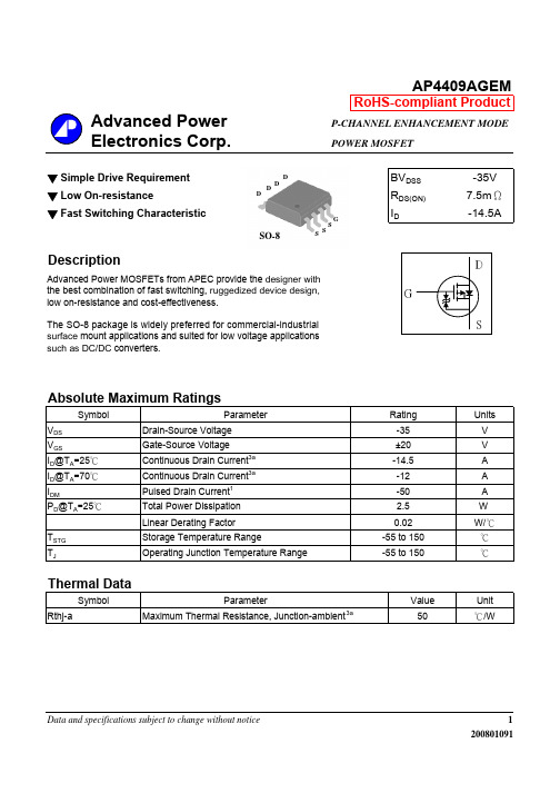
D D D D
SO-8
G S SS
Description
Advanced Power MOSFETs from APEC provide the designer with the best combination of fast switching, ruggedized device design, low on-resistance and cost-effectiveness.
-35 -
-
V
-
- 7.5 mΩ
-
- 15 mΩ
-1 - -3 V
-
7
-
S
-
- -10 uA
-
- -25 uA
-
- ±30 uA
- 58 90 nC
-
7
- nC
- 37 - nC
- 15 - ns
- 13 - ns
- 76 - ns
- 60 - ns
- 4100 6600 pF
- 640 - pF
- 530 - pF
BVDSS RDS(ON)
VGS(th) gfs IDSS
IGSS Qg Qgs Qgd td(on) tr td(off) tf Ciss Coss Crss
Drain-Source Breakdown Voltage Static Drain-Source On-Resistance2
Gate Threshold Voltage Forward Transconductance
0.01 0.01
0.1
1
10
-V DS , Drain-to-Source Voltage (V)
1s DC
MSDS_ACT940

灭火方法和灭火剂:泡沫、二氧化碳、干的化学制品
灭火注意事项:穿戴正压呼吸器和备有抗化学物的全副保护衣。
第六部分 泄漏应急处理
应急处理:大量外漏时,迅速报警、疏散有关人员、隔离污染区,排除所有易燃的根源(火焰、信号灯火焰及电火花)。慎防与排出的液体、下水沟、水道或其他水源接触。如果发生水污染,通知有关当局。
医生须知:
这一种吸入性危险物料。在决定是否以呕吐方法时,必须考虑吸入性物料引起口腔中毒的潜在可能性(参第3部分-吞食)。以下器官(或器官系统)的紊乱可能会因接触该物料而恶化;器官包括皮肤、肺(如气喘病)、肝及肾。
第五部分 消防措施
危险特性:水汽较空气重并可以沿地面进行或被空气流动而移动及因受热、信号灯、其他火焰或在物料处理点以外的火源而着火。不要在钢筒(就算是空置的)上或附近使用焊接或切断手电筒,因为物品(尽管只剩下一点)会爆发性地着火。
避免接触的条件:无资料
聚合危害:不会进行危险性聚合作用
分解产物:二氧化碳及一氧化碳,各种碳氢化合物
第十一部分 毒理学资料
急性毒性:无资料
亚急性和慢性毒性:--
刺激性:无资料
致敏性:--
致突变性:--
致畸性:--
致癌性:并没有相关资料。因该种物料导致致癌症的可能性不明。此物料并未被列入国际癌症研究机构的全国毒物计划或职业安全卫生署内。
OSHA VPEL 5.000ppm-TWA(皮肤) ACGIH TLV 5.000ppm-TWA(皮肤)
监测方法:无资料
工程控制:提供重要的技术性通分系统以将曝光机会保持在低于TLV 水平
呼吸系统防护:如果工作地点的物品及成分超过标准,在无法完善控制环境时,建议使用符合NIOSH/MAHA规格的呼吸防护具。在特定情况下,OSHA规格同时包括其他NIOSH/MSHA氧气口罩(负压式设计)(请查询卫生安全指导)。应实施技术及行政上的监控以减少曝露的机会。
电子器件中文资料

下边资料的次序是纳米盘上的自动排列,请需要者自己看着找吧。
最后还有07年全年的《读者》E书下载,及几个小游戏。
4000系列数字集成电路资料大全.4000.rar/d/7d8425c10a0ff161c3e0e00037737a69c5d3980411432404AD620中文资料.pdf/d/b1961b23b272d8531b9f390fa570ae2c71c2d45024a6050074系列数字集成电路手册大全.pdf/d/b4c283d67d1af4aacf7b7c19d3d5aa3b71a8c58d7692c801速查速用世界可控硅代换手册.pdf/d/be70c47f9fc76db61c62e1caf90d0f4a87d1a68459699901最新集成电路应用300例.rar/d/365971ce99cae66629dd2d76d45b0307e83a21d461b83900怎样使用运算放大器.pdf/d/8ca6ba96b0a2d9d8ed0023ecde54908c909fb5cc8c8e2900新型实用电路制作200例.rar/d/b9f585eb5512f27c380fc3e01ce465e105592c00548f7d00新型电子电路应用实例精选.rar/d/2cd40d687adff1a0031927956c3ae4b16bd41b6489d48e00电子线路设计应用手册.rar/d/86601a2c9c3d346da2b7582806c525fc91e3cf55109a6301新编电子电路大全.rar/d/0ed4b1cba5ad94a5bdfabd410aae1c058c2bbd65aa8f6e00电子电路及电子器件.rar/d/0856a0265ffdc5947a7a4fe93ea34fa53539165b851ea700数字电路.rar/d/00fca0f91805c0f137bcfdc966caba0297c0e6d7dd4c3b00实用双向可控硅应用500例.rar/d/3ebb740d73718fb3cda67b20cb2d50620430f264cc2d6a00实用电子线路集.rar/d/4873ecc0445c91c3d7b444d6b71056bd6b45dc89ef6b8100实用电子电路大全.rar/d/2ca46fb365cedaee9451b79c697e8ff474d22aa6c5ebaf00实用单元电路及其应用.rar/d/3c77fff6e45fddf87dee1bf7788a1c242b1d1c4ef9119600三极管资料大全.rar/d/00de8710ba6c1e8c289ecaf61208d6b6ea32504677a90000绝对精品的硬件设计方面资料.rar/d/c8d1606af74af0a6f7a7f414376c7137e200fb588e460600简易可控硅整流电源电路.pdf/d/28430231e150b19c1d91d1a52f0104a8fef4b07eee510000电子电路大全(合订本).rar/d/7c041e86b457278bc289756622eca10562b31d68f6ba7a01电子电路集.pdf/d/cc133c04fb2ebe2abc1ed4b2a363046e6bff0d2bf8c04100电子电路百科全书(第五卷).rar/d/18148ed5200f99e6176c888024eb8e72d323fcf3e2007900电子电路.pdf/d/f1836309214f28fd8227efa0969e0d39c5261f29c88d4400电子爱好者实用电子制作.rar/d/05edad0c1b9b9c98eabc2847ca8a5d4cfa4fea48d9331f00常用电子元气件手册.pdf/d/f42c221af44585fee096c2b2c3f5d5da87591f3a7a143600常用电子元器件图片.pdf/d/90f6611e31ac9f60a761abb7af0ba31f50fb5a2a781f1c00常用稳压芯片篇.txt/d/6224bdf4fe9e168d36f3ef223422b6add262a8ed810c0000常用电子元器件简明手册.rar/d/00b9d1eedddd798047798152c65d916e257ff4e277702300常用电子元气件命名.pdf/d/3c89dc7fbb8fd14f64b93d946f16583a5c0c3848ce720800P8xC591_cn.pdf/d/8e6c43250690dc6baee98e3865798ee4fc85f5724ba14d00MAX485中文资料.pdf/d/15b701ca1ffd126726fdf070ea1f018d8344aa8bf19c0d00MAX280中文资料.pdf/d/12a35473a7bb0afbb25d41f079b2cbd5af770460877b0100MAX194中文资料.pdf/d/c4a65303e4422f2b661ee713c44e3000ab1ec8baf34b0100T8变压器.pdf/d/86d97d9ca03ec16cb94e885a63912561864f0dfb384d0200NE555.pdf/d/6eeb2db556192e988d3f45d6fc6a976d3743a54695d40300LM7805中文资料.pdf/d/20ade1675d2aebb22a5b7e8596cf421ad74fb6e0bc680400NE555中文资料.pdf/d/4437cbafdb450d9803022a7f145806736178b2647d8e0000MC1413.pdf/d/a8b41856cce7d8c13e68d7be0f7eba717d00bcc2be460100MCP3202中文资料.pdf/d/e6652d4504073a352f4a6e628575bcb68cd4b7bac3ed0b00MC3423.PDF/d/1856c527d115fecf23c7cc792b2df521f434795f4ad80100LM358中文资料.pdf/d/01055a8e69fd7f39469037ab678f9ed4a2807672378c0100LM339.rar/d/8c8b06f70cccad70c338f9f8bb9bf85745f5340af9480000lm2596.pdf/d/67de0105031f80ad657a9558635c3a8b38140cc53ada0c00LM2576中文资料.pdf/d/fc5567b2fa37f7ce88b5272536b2d817eb231c50971e0400lm1117中文资料.pdf/d/f24586db9afc12e7f9bf32371f24b389452a1cc4a7bb0b00LM393中文资料.pdf/d/1961b1559934b7bf617ae57027e87ebb7d12aea50a9a0300LM363中文资料.pdf/d/7e83da8b44365c274829b181ecf725a2291407804cb40100LM7909中文资料.pdf/d/8ce4617cb1123fda1ad10ad38d4493a6480e86f5d4bf0000LMD18200.doc/d/a7e301b93175eb71345299272395fce9e06a30a8009c0100lm324中文资料.pdf/d/cc590a103a433200fdfb3a57f44f5f383d2ee0b4557d0a00LM317中文资料.pdf/d/686a9606b1dd1cca239d8a6bcc8e27d4b45c1f8c24d50d00lm211lm311中文资料.pdf/d/eb9f6ebac497c099445f95a4ad95a0a44730341a715d0b00LM140.pdf/d/3876aea02373e492cdb7da633c9ba26d5f250e06d8e10200LM358.pdf/d/7816ffab592a9e37d9c493dd238fc6b6e55397be8e5e0100LM109.pdf/d/a70eaf6138bb71be74d0431224cbd5d0c7f1136a55740100lm3s317_ds_cn.pdf/d/bd34bf2a2ab69f935911e60206bd5e1a67e6f06ca0215d00 LF398中文资料.pdf/d/bcd8edd55f76babe047e7e1e8e61045af8129ab1866e0100L290-L291-L292.pdf/d/2e0ab9638f84016c18a6ff0fc817b8dbf1043857e30b0400ICL7135中文资料.pdf/d/71e1b23dbc5dff6f6fef9c002be6420f5968745750710800ICL7104中文资料.pdf/d/e07abec1e557ad53c159d7156237bfa86e842cb549820100fm3135_ds.pdf/d/fc97032bc0142c568bdd39f8140d82c6ae4ee9b175260400cd40161中文资料pdf.pdf/d/40230b71ccbbc78b9355e8946d1e4391efecf2199da10200最新世界三极管特性代换手册.r/d/6605148cde3dddb2a4bb9123eb0dcdb6721a053f286c7601lm3s310_ds_cn.pdf/d/bb01eb82cbddbc6fabae95b5a3f631f1d32d3331750e5700cmos4000器件中文资料.pdf/d/bde8cef1903e5f776ddae591fe4b9fe4dd41fa2023074800cd40109中文资料pdf.pdf/d/202883c137a9443ae5aad82ac01c0c5d5b027bfceeb50100cd40105中文资料pdf.pdf/d/b56e06f4a9b172b10908429505b829f1b06b46934bca0100ds1302中文资料.pdf/d/8ffe86b97d76a8cc3fffe2b8b7d7d411ea84ad0bac730300cd40163中文资料pdf.pdf/d/305f9eca8225b8333aafa3a1bd0c4c3c1c3ac34338a10200cd40147中文资料pdf.pdf/d/e3380153eb1198bc857e579999fc3dddb55b460294f20100cd4076中文资料.pdf/d/d000f62e7c0c80c37332f73d5a9200afa8a7f4b572f30200cd4071中文资料.pdf/d/49f8cce83e6ab3e4d593fa45e1f0e685dcbb5186db3a0200cd4070中文资料.pdf/d/82edf36cc8617e3356612ac573e356ba89959470a3420200cd4068中文资料.pdf/d/18c87ad5f8690c9cd1a33121bfd1ba3040256c7d8f490200cd4067中文资料.pdf/d/e6966eea3a191a3186dd7bfb5f19f031b430ea7121530200cd4055中文资料.pdf/d/33d92d1285e92130dbb263df34bebe04f1418d98e29f0300cd4038中文资料.pdf/d/bebc590afbebe766436886d23fbc5205344cbe07d5690300cd4029中文资料pdf.pdf/d/0d4dc7d75ded5885fd3e475e8071f438921d796cbd750400cd4048中文资料.pdf/d/846d38f344ce9ef88598d6e69a542300fed3c3d7d33f0200cd4047中文资料.pdf/d/36a5eec356ffc0baf497d07e71f28081732d28bc145e0200cd4035中文资料.pdf/d/c7b4075b5bda2910cbfdc61bd13730a2d7ab41f161a10300cd4034中文资料.pdf/d/b6dadf2ee2883540208c0f0e06d930fbbf0812016faf0400cd4028中文资料pdf.pdf/d/557cd672fe94a58e1e0c7b508bd095c74c7851d7fb820300cd4024中文资料pdf.pdf/d/c2196481f081938dbb92ed67395098e681fac3206cf10300cd4027中文资料pdf.pdf/d/348e802290198d2503df1013653fd744b97ccdba31ef0200 AT89S51.pdf/d/dccdecb6e6192d5581e790a27bf787eb9a354e1335350900cd4053.pdf/d/404342f322a3a932c98775f207d3ebfd4086551dacb10200cd4034中文资料.pdf/d/49106b6ade07c448f2e9f0d4c232dd8f818961bf6faf0400cd4028中文资料pdf.pdf/d/21e60f5ad93242cad1720458dce6b23333765ec7fb820300cd4027中文资料pdf.pdf/d/60d154cb4a834783bdc59afd3385cd025*********ef0200cd4022中文资料pdf.pdf/d/1057c76c8deff8300c6a6db430ba3282d53d9dbfc70d0400att7021cn.pdf/d/0e5d65285c35682e713bddf0a405e0326a64aba2c6c20a00BA5101BA5201.pdf/d/5d16c3c4e4ac5e156c4241ea590dba00ef7246403acf0400AT89S51.pdf/d/237f01593ba5bddc8665e29116ff139e19c340d435350900AT89LV52.pdf/d/5879e4ac095f60ca5e2b92beb242eaac1c5665cedf300800ad9850中文资料.pdf/d/38a283d55c2c6ceb04694c7a5534c3ae16ab96a6dc6e1c00AT89C1051U.pdf/d/559f6cf5bc2aefa3bbaf4bc6d6f9dd17042dcba1f8d40400 AD673.pdf/d/559f6cf5bc2aefa3bbaf4bc6d6f9dd17042dcba1f8d40400AD620中文资料.pdf/d/145656a8efc258c014c5330ed03482a33a04ea6524a60500AD594_595.pdf/d/6028f9ccfdf02af289e312c94ef8cfc0d9275efdb6220200AD346中文资料.pdf/d/7bd0a4417a8213a7dc982986fbcdae8ce53d9e53fa4401009013.pdf/d/9057c57766e0d1fded4e6a49804e23949c2177bc6d9501008050.pdf/d/24e3b9655ebf0b2f019abd07baaa995fa98f45bf31a1020078xx.pdf/d/af10e44a0a8b804bdd6336b88e2188cf195375644b1c010074LS164中文资料.pdf/d/201383c7b23d7057d102cfc148946d045797b4a88914030074ls245中文资料.pdf/d/37f26e3d5349c02dc216bdc7a487060d1332e94f7501030074LS138中文资料.pdf/d/52f4c8c7b39181704008ceb6e89ea8095faaab98cbbe030074ls138.PDF/d/7aa7e214ce5dfe4c5dce8d9c78ab396289ca517377b9030074ls74.PDF/d/9e1051ab95e509fe3414830be349e6d7d6f56374297a060074ls04.PDF/d/e8a4bad83b00a61a514f295ef7d36aa064801b744472040074LS14中文资料.pdf/d/8938dbc43cdb1a232112a8f69e0b0f7e50357cb54389030074HC245中文资料.pdf/d/d045498e1b5a8b831fb554e3059f7c9c6a3ed92d1701030024c02中文官方资料手册pdf.pdf/d/5463179db3bbb8a494d38f0ab48c8cbb9cf6aece299c090074ALS245.pdf/d/b4c462102ac87887e8e5059e001f16647c213459b13f01004N25中文资料.pdf/d/c818ecf73638d05fb5489690e28b91c94c0976af7ccb0100USB DISK EJECT.EXE/d/4102ee837c5b11d7d7e3d40c759bd5b384154f33007c0d00TEA1062.pdf/d/569c7b2bf61ebf2e2c01d7fcb3bdb0a3f1b83a0d8b4e030078xx.pdf/d/dc3547b7951a28c30c447002adfc743b2cd8174a4b1c010074ls245中文资料.pdf/d/f0fd2d9a704cfc09571d7f694b8e5625ea2577f57501030074LS138中文资料.pdf/d/8df689b9e0e1157387ae34ffb186587654607dc5cbbe030074ls138.PDF/d/906f5068200722722dd009f2c0558d2ca954855d77b9030074ls74.PDF/d/d4ce35981359c38e4e10a143913dbc77ec41b17c297a060074LS14中文资料.pdf/d/500d0dd2c24ca57fdd5f81887ce014ee383cf15f4389030074ls04.PDF/d/00b330534fc4824625e3f5aadb970e2cb07c17204472040024c02中文官方资料手册pdf.pdf/d/0dfded751578a730e85acec4fecb3ff3ecb3e344299c090074HC245中文资料.pdf/d/ff5c91227f1bf663c1326fc19d5295f02035768b1701030074ALS245.pdf/d/0347de88ba42c7981ec9d8cb0829ed27dee125a8b13f01001N4148smd.pdf/d/885391bb8724b237c52840be7996214047193380cfa008002n4403.PDF/d/20bc155264d25b57a981c63afab4b0be6bb806f2b4f700002n4401.PDF/d/40c749e3a06284cca55f4964a1322308e344b26651f70000LMD18200.doc/d/58c3a544b3cc4481889d5c85b54087756849a92e009c0100。
- 1、下载文档前请自行甄别文档内容的完整性,平台不提供额外的编辑、内容补充、找答案等附加服务。
- 2、"仅部分预览"的文档,不可在线预览部分如存在完整性等问题,可反馈申请退款(可完整预览的文档不适用该条件!)。
- 3、如文档侵犯您的权益,请联系客服反馈,我们会尽快为您处理(人工客服工作时间:9:00-18:30)。
Electronics
Computer Cable
Product Construction:
Conductor:
• 28 and 24 AWG fully annealed stranded
tinned copper per ASTM B-33
Insulation:
• Premium-grade, coIor-coded S-R PVC
per UL 1061
• Color Code: See charts below
Shield:
• 100% Flexfoil®aluminum/polyester
with 25% overlap, minimum, foil facing out
• Stranded tinned copper drain wire
(28 AWG only)
• 65% tinned copper braid
Jacket:
• PVC, gray
• Temperature Range: –20˚C to +80˚C
Applications:
• Computers
• Industrial equipment
• Data transmission
• Control circuits
• Suitable for EIA RS-232 applications
• Suggested voltage rating: 300 volts
Features:
• Braid shield provides good flexibility
• Superior shielding where noise rejection
is critical
• Assists system designers in meeting FCC
Docket 20780 demands
Compliances:
• NEC Article 725 Type CL2 - 28 AWG
(UL: 75˚C)
• NEC Article 800 Type CM - 24 AWG
(UL: 75˚C)
• UL Style 2464 (UL: 80°C, 300V)
• CSA CMG (CSA: 60˚C)
• Designed to meet UL 70,000 BTU Vertical
Tray Flame Test
• Passes CSA CMG Flame Test
Packaging:
• Please contact Customer Service for
packaging and color options Multi-Conductor, Foil/Braid Shield
UL 2464, NEC Type CL2 or CM (UL) c(UL), CSA CMG
**B - Capacitance between one conductor and other conductors connected to shield
*Color Code Chart 1. Remaining items Color Code Chart 2
元器件交易网
41
Computer Cable Electronics Multi-Conductor, Foil/Braid Shield
UL 2464, NEC Type CM (UL) c(UL), CSA CMG
Product Construction:
Conductor:
• 22 AWG fully annealed stranded tinned
copper per ASTM B-33
Insulation:
• Premium-grade, coIor-coded S-R PVC
per UL 1061
• Color Code: See chart below
Shield:
• 100% Flexfoil®aluminum/polyester
with 25% overlap, minimum, foil facing out
• 65% tinned copper braid
Jacket:
• PVC, gray
• Temperature Range: –20°C to +80˚C
Applications:
• Computers
• Industrial equipment
• Data transmission
• Control circuits
• Suitable for EIA RS-232 applications
• Suggested voltage rating: 300 volts
Features:
• Braid shield provides good flexibility
• Superior shielding where noise rejection
is critical
• Assists system designers in meeting FCC
Docket 20780 demands
Compliances:
• NEC Article 800 Type CM (UL: 75˚C)
• UL Style 2464 (UL: 80°C, 300V)
• CSA CMG (CSA: 60˚C)
• Designed to meet UL 70,000 BTU Vertical
Tray Flame Test
• Passes CSA CMG Flame Test
Packaging:
• Please contact Customer Service for
packaging and color options
*B - Capacitance between one conductor and other conductors connected to shield 元器件交易网
42。