LT6011IMS8#PBF中文资料
常见IMS报错信息
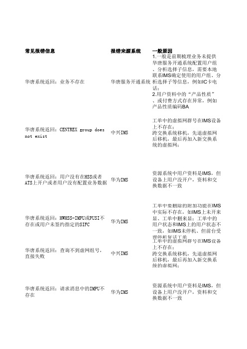
常见报错信息报错来源系统一般原因华唐系统返回:业务不存在华唐服务开通系统1.一般是前期梳理业务未提供华唐服务开通系统配置用户组、分析选择子信息,需要本地联系IMS确定使用的用户组、分析选择子等信息,例如IC卡电话;2.用户资料中的“产品性质”、或付费方式存在异常,例如产品性质编码BA华唐系统返回:CENTREX group does not exist 中兴IMS工单中的虚拟网群号在IMS设备上不存在;跨交换系统移机,先退虚拟网后移机,最后再加入新交换系统的虚拟网;华唐系统返回:用户没有在HSS或者ATS上开户或者用户没有配置业务数据华为IMS资源系统中用户资料是IMS,但设备上用户没开户,资料和交换数据不一致华唐系统返回:HWHSS-IMPU或PUSI不存在或用户未签约指定的SIFC 华为IMS工单中要删除的附加功能在IMS中实际不存在,如IMS上未开来显、工单中删来显;工单中的用户状态和IMS上的用户状态不一致,如IMS未停机、但前台受理停机复话工单华唐系统返回:查询不到虚网组号,直接失败中兴IMS工单中的虚拟网群号在IMS设备上不存在;跨交换系统移机,先退虚拟网后移机,最后再加入新交换系统的虚拟网;华唐系统返回:请求消息中的IMPU不存在华为IMS资源系统中用户资料是IMS,但设备上用户没开户,资料和交换数据不一致华唐系统返回:SH:User is unknown中兴IMS 1. 资源系统中用户资料是IMS,但设备上用户没开户,资料和交换数据不一致;2.或者是上一笔失败单数据没有回退,导致本次工单执行失败华唐系统返回:网关节点号(HOSTNODEID)]不能为空中兴IMS资源系统数据问题,缺少节点号华唐系统返回:指定的Centrex群不存在华为IMS工单中的虚拟网群号在IMS设备上不存在;跨交换系统移机,先退虚拟网后移机,最后再加入新交换系统的虚拟网;华唐系统返回:TID名称已经存在中兴IMS“节点号+端口号”这个组合在IMS上存在用华唐系统返回:节点号不能为空中兴IMS ONU上的节点号数据有误华唐系统返回:TID名称(A0)已经存在中兴IMS“节点号+端口号”这个组合在IMS上存在用华唐系统返回:没有找到参数%GwIp%的值华唐服务开通系统资源系统中资料不正确华唐系统返回:没有找到参数%用户组%的值华唐服务开通系统华唐没有配置对应的用户组参数华唐系统返回:HSS重号中兴IMS、华为IMS重复在IMS上开户华唐系统返回:没有找到参数%主引示号%的值报告没有匹配到任何成功或失败标志华唐未对所有的报错信息进行配置华唐系统返回:HWHSS-IMPU或PUSI不存在或用户未签约指定的SIFC华为IMS用户号码不存在,或者用户数据不完整处理方法补充说明异常竣工单处理1. 在用户资料无误的前提下,本地联系IMS一同确定参数后,发华唐配置;2. 若是用户资料存在问题,则需要撤单退单后,先在ESS的固网产品及属性变更中对用户的产品性质进行更正。
LINEAR TECHNOLOGY LT6011 LT6012 说明书

100µs/DIV6011 TA0312ELECTRICAL CHARACTERISTICSThe ● denotes the specifications which apply over the full operating temperature range, otherwise specifications are at T A = 25°C. V S = 5V, 0V; V CM = 2.5V; R L to 0V; unless otherwise specified. (Note 5) SYMBOL PARAMETER CONDITIONS MIN TYP MAX UNITS V OS Input Offset Voltage (Note 8)LT6011AS8, LT6012AS2060µVT A = 0°C to 70°C●85µVT A = –40°C to 85°C●110µVLT6011ADD, LT6012AGN2585µVT A = 0°C to 70°C●135µVT A = –40°C to 85°C●170µVLT6011S8, LT6012S2575µVT A = 0°C to 70°C●100µVT A = –40°C to 85°C●125µVLT6011DD, LT6012GN, LT6011MS830125µVT A = 0°C to 70°C●175µVT A = –40°C to 85°C●210µV ∆V OS/∆T Input Offset Voltage Drift (Note 6)LT6011AS8, LT6011S8, LT6012AS,LT6012S●0.20.8µV/°CLT6011ADD,LT6011DD, LT6012AGN,LT6012GN, LT6011MS8●0.2 1.2µV/°C I OS Input Offset Current (Note 8)LT6011AS8, LT6011ADD, LT6012AS,LT6012AGN20300pAT A = 0°C to 70°C●450pAT A = –40°C to 85°C●600pALT6011S8, LT6011DD, LT6012S,LT6012GN, LT6011MS8150900pAT A = 0°C to 70°C●1200pAT A = –40°C to 85°C●1500pA I B Input Bias Current (Note 8)LT6011AS8, LT6011ADD, LT6012AS,LT6012AGN20±300pAT A = 0°C to 70°C●±450pAT A = –40°C to 85°C●±600pALT6011S8, LT6011DD, LT6012S,LT6012GN, LT6011MS8150±900pAT A = 0°C to 70°C●±1200pAT A = –40°C to 85°C●±1500pA Input Noise Voltage0.1Hz to 10Hz400nV P-P e n Input Noise Voltage Density f = 1kHz14nV/√Hz i n Input Noise Current Density f = 1kHz, Unbalanced Source Resistance0.1pA/√Hz R IN Input Resistance Common Mode, V CM = 1V to 3.8V10120GΩDifferential20MΩC IN Input Capacitance4pF V CM Input Voltage Range (Positive)Guaranteed by CMRR● 3.84V Input Voltage Range (Negative)Guaranteed by CMRR●0.71V CMRR Common Mode Rejection Ratio V CM = 1V to 3.8V●107135dB Minimum Supply Voltage Guaranteed by PSRR● 2.4 2.7V PSRR Power Supply Rejection Ratio V S = 2.7V to 36V, V CM = 1/2V S●112135dB A VOL Large-Signal Voltage Gain R L = 10k, V OUT = 1V to 4V●3002000V/mVR L = 2k, V OUT = 1V to 4V●2502000V/mV Channel Separation V OUT = 1V to 4V●110140dB360112fbELECTRICAL CHARACTERISTICSThe ● denotes the specifications which apply over the full operating temperature range, otherwise specifications are at T A = 25°C. V S = 5V, 0V; V CM = 2.5V; R L to 0V; unless otherwise specified. (Note 5) SYMBOL PARAMETER CONDITIONS MIN TYP MAX UNITS V OUT Maximum Output Swing No Load, 50mV Overdrive3555mV (Positive, Referred to V+)●65mVI SOURCE = 1mA, 50mV Overdrive120170mV●220mVMaximum Output Swing No Load, 50mV Overdrive4055mV(Negative, Referred to 0V)●65mVI SINK = 1mA, 50mV Overdrive150225mV●275mVI SC Output Short-Circuit Current (Note 3)V OUT = 0V, 1V Overdrive, Source1014mA●4mAV OUT = 5V, –1V Overdrive, Sink1021mA●4mA SR Slew Rate A V = –10, R F = 50k, R G = 5k0.060.09V/µsT A = 0°C to 70°C●0.05V/µsT A = –40°C to 85°C●0.04V/µs GBW Gain Bandwidth Product f = 10kHz250330kHz●225kHz t s Settling Time A V = –1, 0.01%, V OUT = 1.5V to 3.5V45µs t r, t f Rise Time, Fall Time A V = 1, 10% to 90%, 0.1V Step1µs ∆V OS Offset Voltage Match (Note 7)LT6011AS8, LT6012AS50120µVT A = 0°C to 70°C●170µVT A = –40°C to 85°C●220µVLT6011ADD, LT6012AGN50170µVT A = 0°C to 70°C●270µVT A = –40°C to 85°C●340µVLT6011S8, LT6012S50150µVT A = 0°C to 70°C●200µVT A = –40°C to 85°C●250µVLT6011DD, LT6012GN, LT6011MS860250µVT A = 0°C to 70°C●350µVT A = –40°C to 85°C●420µV ∆I B Input Bias Current Match (Note 7)LT6011AS8, LT6011ADD, LT6012AS,LT6012AGN50600pAT A = 0°C to 70°C●900pAT A = –40°C to 85°C●1200pALT6011S8, LT6011DD, LT6012S,LT6012GN, LT6011MS81800pAT A = 0°C to 70°C●2400pAT A = –40°C to 85°C●3000pA ∆CMRR Common Mode Rejection Ratio●101135dB Match (Note 7)∆PSRR Power Supply Rejection Ratio●106135dB Match (Note 7)I S Supply Current per Amplifier135150µAT A = 0°C to 70°C●190µAT A = –40°C to 85°C●210µA460112fbELECTRICAL CHARACTERISTICS The ● denotes the specifications which apply over the full operating temperature range, otherwise specifications are at T A = 25°C. V S = ±15V, V CM = 0V, R L to 0V, unless otherwise specified. (Note 5) SYMBOL PARAMETER CONDITIONS MIN TYP MAX UNITS V OS Input Offset Voltage (Note 8)LT6011AS8, LT6012AS30135µVT A = 0°C to 70°C●160µVT A = –40°C to 85°C●185µVLT6011ADD, LT6012AGN35160µVT A = 0°C to 70°C●210µVT A = –40°C to 85°C●225µVLT6011S8, LT6012S35150µVT A = 0°C to 70°C●175µVT A = –40°C to 85°C●200µVLT6011DD, LT6012GN, LT6011MS840200µVT A = 0°C to 70°C●250µVT A = –40°C to 85°C●275µV ∆V OS/∆T Input Offset Voltage Drift LT6011AS8, LT6011S8, LT6012AS, LT6012S●0.20.8µV/°C (Note 6)LT6011ADD, LT6011DD, LT6012AGN, LT6012GN, LT6011MS8●0.2 1.3µV/°C I OS Input Offset Current (Note 8)LT6011AS8, LT6011ADD, LT6012AS LT6012AGN20300pAT A = 0°C to 70°C●450pAT A = –40°C to 85°C●600pALT6011S8, LT6011DD, LT6012S, LT6012GN, LT6011MS8150900pAT A = 0°C to 70°C●1200pAT A = –40°C to 85°C●1500pA I B Input Bias Current (Note 8)LT6011AS8, LT6011ADD, LT6012AS, LT6012AGN20±300pAT A = 0°C to 70°C●±450pAT A = –40°C to 85°C●±600pALT6011S8, LT6011DD, LT6012S, LT6012GN, LT6011MS8150±900pAT A = 0°C to 70°C●±1200pAT A = –40°C to 85°C●±1500pA Input Noise Voltage0.1Hz to 10Hz400nV P-P e n Input Noise Voltage Density f = 1kHz13nV/√Hz i n Input Noise Current Density f = 1kHz, Unbalanced Source Resistance0.1pA/√Hz R IN Input Resistance Common Mode, V CM = ±13.5V50400GΩDifferential20MΩC IN Input Capacitance4pF V CM Input Voltage Range Guaranteed by CMRR●±13.5±14V CMRR Common Mode Rejection V CM = –13.5V to 13.5V115135dB Ratio●112135dB Minimum Supply Voltage Guaranteed by PSRR●±1.2±1.35V PSRR Power Supply Rejection Ratio V S = ±1.35V to ±18V●112135dBA VOL Large-Signal Voltage Gain R L = 10k, V OUT = –13.5V to 13.5V10002000V/mV●600V/mVR L = 5k, V OUT = –13.5V to 13.5V5001500V/mV●300V/mVChannel Separation V OUT = –13.5V to 13.5V●120140dB V OUT Maximum Output Swing No Load, 50mV Overdrive4580mV (Positive, Referred to V+)●100mVI SOURCE = 1mA, 50mV Overdrive140195mV●240mVMaximum Output Swing No Load, 50mV Overdrive4580mV (Negative, Referred to V–)●100mVI SINK = 1mA, 50mV Overdrive150250mV●300mV560112fb660112fbI SCOutput Short-Circuit Current V OUT = 0V, 1V Overdrive (Source)1015mA (Note 3)●5mA V OUT = 0V, –1V Overdrive (Sink)1020mA ●5mA SRSlew RateA V = –10, R F = 50k, R G = 5k 0.080.11V/µs T A = 0°C to 70°C ●0.07V/µs T A = –40°C to 85°C ●0.05V/µs GBW Gain Bandwidth Product f = 10kHz275350kHz ●250kHz t s Settling TimeA V = –1, 0.01%, V OUT = 0V to 10V 85µs t r , t f Rise Time, Fall TimeA V = 1, 10% to 90%, 0.1V Step 1µs ∆V OSOffset Voltage Match (Note 7)LT6011AS8, LT6012AS 50270µV T A = 0°C to 70°C ●320µV T A = –40°C to 85°C●370µV LT6011ADD, LT6012AGN 50320µV T A = 0°C to 70°C ●420µV T A = –40°C to 85°C ●450µV LT6011S8, LT6012S 70300µV T A = 0°C to 70°C ●350µV T A = –40°C to 85°C●400µV LT6011DD, LT6012GN, LT6011MS880400µV T A = 0°C to 70°C ●500µV T A = –40°C to 85°C●550µV ∆I BInput Bias Current Match (Note 7)LT6011AS8, LT6011ADD, LT6012AS, LT6012AGN 50600pA T A = 0°C to 70°C ●900pA T A = –40°C to 85°C●1200pA LT6011S8, LT6011DD, LT6012S, LT6012GN,LT6011MS81800pA T A = 0°C to 70°C ●2400pA T A = –40°C to 85°C●3000pA ∆CMRR Common Mode Rejection Ratio ●109135dB Match (Note 7)∆PSRR Power Supply Rejection Ratio ●106135dBMatch (Note 7)I SSupply Currentper Amplifier 260330µA T A = 0°C to 70°C ●380µA T A = –40°C to 85°C●400µAELECTRICAL CHARACTERISTICSThe ● denotes the specifications which apply over the full operatingtemperature range, otherwise specifications are at T A = 25°C. V S = ±15V, V CM = 0V, R L to 0V, unless otherwise specified. (Note 5)Note 1: Stresses beyond those listed under Absolute Maximum Ratings may cause permanent damage to the device. Exposure to any Absolute Maximum Rating condition for extended periods may affect device reliability and lifetime.Note 2: The inputs are protected by back-to-back diodes and internal series resistors. If the differential input voltage exceeds 10V, the input current must be limited to less than 10mA.Note 3: A heat sink may be required to keep the junction temperature below absolute maximum ratings.Note 4: Both the LT6011C/LT6012C and LT6011I/LT6012I are guaranteed functional over the operating temperature range of –40°C to 85°C.Note 5: The LT6011C/LT6012C are guaranteed to meet the specified performance from 0°C to 70°C and is designed, characterized and expected to meet specified performance from –40°C to 85°C but is not tested or QA sampled at these temperatures. The LT6011I/LT6012I are guaranteed to meet specified performance from –40°C to 85°C.Note 6: This parameter is not 100% tested.Note 7: Matching parameters are the difference between any two amplifiers. ∆CMRR and ∆PSRR are defined as follows: (1) CMRR and PSRR are measured in µV/V for the individual amplifiers. (2) The difference between matching amplifiers is calculated in µV/V. (3) The result is converted to dB.Note 8: The specifications for V OS , I B , and I OS depend on the grade and on the package. The following table clarifies the notations.SYMBOL PARAMETERCONDITIONSMIN TYP MAXUNITS STANDARD GRADEA GRADE S8 Package LT6011S8LT6011AS8DFN Package LT6011DD LT6011ADD S14 Package LT6012S LT6012AS GN16 Package LT6012GN LT6012AGN MS8 PackageLT6011MS8N/A760112fbTIME (SEC)0N O I S E V O L T A G E (0.2µV /D I V )86011 G092461071359V S = ±15V T A = 25°C8THD + Noise vs FrequencyOutput Saturation Voltage vs Load Current (Output Low)LOAD CURRENT (mA)0.010.11106011 G13T A = 85°CT A = 25°CV S = 5V, 0VT A = –40°CTIME (SEC)N O I S E V O L T A G E (0.2µV /D I V )806011 G102040601007010305090V S = ±15V T A = 25°C91060112fbSmall-Signal Transient ResponseLarge-Signal Transient ResponseRail-to-Rail Output Swing20mV/DIVA V = 12µs/DIV6011 G282V/DIV A V = –150µs/DIV6011 G29V S = ±15V1V/DIVA V = –1100µs/DIV6011 G30V S = 5V, 0VTYPICAL PERFOR A CE CHARACTERISTICSU W0V 0VPreserving Input PrecisionPreserving the input accuracy of the LT6011/LT6012 re-quires that the applications circuit and PC board layout do not introduce errors comparable to or greater than the 25µV typical offset of the amplifiers. Temperature differentials across the input connections can generate thermocouple voltages of 10’s of microvolts so the connections to the input leads should be short, close together and away from heat dissipating components. Air currents across the board can also generate temperature differentials.The extremely low input bias currents (20pA typical) allow high accuracy to be maintained with high impedance sources and feedback resistors. The LT6011/LT6012 low input bias currents are obtained by a cancellation circuit on-chip. This causes the resulting I B + and I B – to be uncorrelated, as implied by the I OS specification being comparable to I B . Do not try to balance the input resistances in each input lead; instead keep the resistance at either input as low as possible for maximum accuracy.Leakage currents on the PC board can be higher than the input bias current. For example, 10G Ω of leakage between a 15V supply lead and an input lead will generate 1.5nA!Surround the input leads with a guard ring driven to the same potential as the input common mode to avoid exces-sive leakage in high impedance applications.Input ProtectionThe LT6011/LT6012 feature on-chip back-to-back diodes between the input devices, along with 500Ω resistors inseries with either input. This internal protection limits the input current to approximately 10mA (the maximum al-lowed) for a 10V differential input voltage. Use additional external series resistors to limit the input current to 10mA in applications where differential inputs of more than 10V are expected. For example, a 1k resistor in series with each input provides protection against 30V differential voltage.Input Common Mode RangeThe LT6011/LT6012 output is able to swing close to each power supply rail (rail-to-rail out), but the input stage is limited to operating between V – + 1V and V + – 1.2V. E xceed-ing this common mode range will cause the gain to drop to zero, however, no phase reversal will occur.Total Input NoiseThe LT6011/LT6012 amplifier contributes negligible noise to the system when driven by sensors (sources) with impedance between 20k Ω and 1M Ω. Throughout this range, total input noise is dominated by the 4kTR S noise of the source. If the source impedance is less than 20k Ω,the input voltage noise of the amplifier starts to contribute with a minimum noise of 14nV/√Hz for very low source im-pedance. If the source impedance is more than 1M Ω, the input current noise of the amplifier, multiplied by this high impedance, starts to contribute and eventually dominate.Total input noise spectral density can be calculated as:v e kTR i R n TOTAL n S n S ()()=++224APPLICATIO S I FOR ATIOWUU U 5V1112131415Information furnished by Linear Technology Corporation is believed to be accurate and reliable.However, no responsibility is assumed for its use. Linear Technology Corporation makes no represen-tation that the interconnection of its circuits as described herein will not infringe on existing patent rights.16Linear Technology Corporation1630 McCarthy Blvd., Milpitas, CA 95035-7417(408) 432-1900 ● FAX: (408) 434-0507 ● © LINEAR TECHNOLOGY CORPORA TION 2003LT 0406 REV B • PRINTED IN USA。
ILI9488_AN_V0.1_20121116
141
142
VCOM
143
144
VCOM VCOM VCOM TESTP_VGP TESTP_VGP AGND/DGND AGND/DGND DUMMY DUMMY DUMMY DUMMY DUMMY MIPI_LDO DUMMY MIPI_DATA_N/MDDI_DATA_N MIPI_DATA_N/MDDI_DATA_N MIPI_DATA_P/MDDI_DATA_P MIPI_DATA_P/MDDI_DATA_P MIPI_CLOCK_N/MDDI_STB_N MIPI_CLOCK_N/MDDI_STB_N MIPI_CLOCK_P/MDDI_STB_P MIPI_CLOCK_P/MDDI_STB_P DUMMY_TEST0 DB23 DB22 DB21 DB20 DB19 DB18 CABC_PWM IM0 IM1 IM2 RESX VSYNC HSYNC DOTCLK ENABLE DB17 DB16 DB15 DB14 DB13 DB12 DB11 DB10 DB9 DB8 DB7 DB6 DB5 DB4 DB3 DB2 DB1 DB0 SDO/DOUT SDA/DIN RDX WRX/SCL D/CX CSX TE IOVCC IOVCC VDD VDD DGND DGND DGND VGS AGND AGND AGND VCOM VCOM VCOM C41A/C15A C41A/C15A C41B/C15B C41B/C15B DUMMY_NVCOR DUMMY_NVCOR VCL/DDVDL VCL/DDVDL DDVDH DDVDH DDVDL/VCL DDVDL/VCL VCI VCI VCI C11B_C31B C11B_C31B C11B_C31B C11B_C31B C11A_C31A C11A_C31A C11A_C31A C11A_C31A C12B_C32B C12B_C32B C12B_C32B C12B_C32B C12A_C32A C12A_C32A C12A_C32A C12A_C32A VGL VGL VGL VGL AGND AGND AGND VGH VGH VGH VGH C51B/C11B C51B/C11B C51B/C11B C51A/C11A C51A/C11A C51A/C11A C52B/C12B C52B/C12B C52B/C12B C52B/C12B C52A/C12A C52A/C12A C52A/C12A C52A/C12A C21B C21B C21B C21B C21A C21A C21A C21A VCOM VCOM VCOM
L1.爱立信告警类型代码汇总
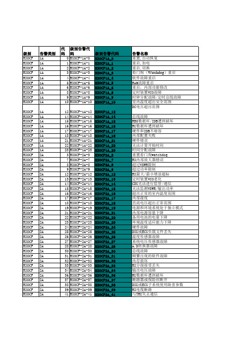
告警类别 1A 1A 1A 1A 1A 1A 1A 1A 1A 1A 1A 1A 1A 1A 1A 1A 1A 1A 1A 2A 2A 2A 2A 2A 2A 2A 2A 2A 2A 2A 2A 2A 2A 2A 2A 2A 2A 2A 2A 2A 2A 2A 2A 2A 2A 2A 2A 2A 2A 2A 2A
2A 2A 2A 2A 2A 2A 2A 2A 2A 2A 2A 2A 2A 2A EXT1B EXT1B EXT1B EXT2B EXT2B EXT2B 无 1B 1B 1B 1B 2A 2A 2A 2A 2A EXT1B EXT1B EXT2B 1A 1A 1A 1A 1A 1A 1A 1A 1A 1A 1A 1A 1A 1A 1A 1A 1A 1A 1A
RXOCF RXOCF RXOCF RXOCF RXOCF RXOCF RXOCF RXOCF RXOCF RXOCF RXOCF RXOCF RXOCF RXOCF RXOCF RXOCF RXOCF RXOCF RXOCF RXOCF RXORX RXORX RXORX RXORX RXORX RXORX RXORX RXORX RXORX RXORX RXOTF RXOTF RXOTF RXOTRX RXOTRX RXOTRX RXOTRX RXOTRX RXOTRX RXOTRX RXOTRX RXOTRX RXOTRX RXOTRX RXOTRX RXOTRX RXOTRX RXOTRX RXOTRX RXOTRX RXOTRX RXOTRX
44 45 46 47 48 49 50 51 52 53 57 58 69 73 2 4 5 6 9 10 无 0 5 9 10 0 1 2 5 6 0 1 1 1 2 3 4 5 6 8 9 12 13 14 15 16 17 20 21 22 23 24
三星 SGH-L608 说明书

使用说明书交通安全第一驾车时不要使用手机。
如要通话,请先停车。
加油时关机在加油站(维修站)或靠近易燃物品、化学制剂的地方,请勿使用手机。
乘坐飞机时要关机移动电话会造成干扰,在飞机上使用手机不仅危险而且是违法的。
在医疗设备附近关机医院或卫生保健机构可能会使用对无线频率敏感的设备。
请有效遵守所有规章或准则。
干扰移动通信可能会受到无线电干扰。
无线电干扰会影响手机的性能。
遵守特殊规定在任何地方都要遵守特殊规定。
在禁止使用手机或可能产生干扰或危险时,必须关闭手机。
防水此手机不能防水,请保持其干燥。
合理使用仅在正常位置(耳边)使用手机。
开机后,不要无故用手触摸手机上端内置天线位置。
紧急呼叫输入当地的紧急呼叫号码。
按键拨打。
手机放置于儿童触摸不到的地方手机和其所有配件(包括附件)应放置于儿童触摸不到的地方。
配件和电池请使用三星公司专用电池和配件(如耳机和PC数据线等)。
使用非三星配件可能会让您受伤或损坏手机,并可能引起危险。
使用三星认可的软件只能使用三星授权的软件。
使用其它未授权的软件可能会损坏您的手机。
授权服务必须由专业人员进行安装或维修。
关于更详细的安全信息,见38页的“健康和安全信息”。
•如果使用与手机不匹配的电池,可能会引起爆炸。
•请按照生产商的说明,处理欲废弃的电池。
长时间以非常高的音量用耳机收听可能会损坏您的听力。
12本说明书简介本使用说明书叙述有关如何使用手机的简明信息。
如欲迅速掌握本手机的基本使用方法,请参照“开始使用”和“特殊功能”。
在本说明书中,有下列指示图标:表示您需要仔细阅读关于安全或手机功能的信息。
→表示您需要按下导航键,滚动到指定的选项,然后选择该选项。
[]表示手机上的按键。
例如,[]。
<>表示软键,手机屏幕上显示该软键的功能。
例如,<功能表>。
3目录配件介绍 6您可能拥有下列配件开始使用 6使用手机的初始步骤手机的安装和充电 (6)开机和关机 (7)手机部位图 (8)按键和图标 (9)使用功能表 (12)输入文本 (12)根据需要设定手机 (15)特殊功能 17开始使用通话功能、照相机、音乐播放器、WAP浏览器和其它特殊功能拨打/接听电话 (17)使用照相机............................................................................. 19播放音乐 (20)收听 FM收音机 (22)浏览Web (23)使用电话簿 (24)发送信息 (25)查看信息 (26)使用蓝牙无线技术 (27)功能表功能 29列出所有功能选项健康和安全信息 384功能表在待机模式且键盘开锁状态下按下<功能表>,进入功能表模式。
松下smt错误代码表
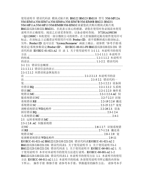
使用说明书错误代码表模块式贴片机BM122 BM123 BM133 型号NM-MF12A NM-EJM5A NM-EJM7A NM-EJM9A NM-EJM7B NM-EJM6B BM221 BM231NM-MF11A NM-MF13 NM-EJM8B NM-EJM1C承蒙您此次购买模块式贴片机BM122/123/133/221/BM231,在此表示衷心的感谢。
请您在使用时务必阅读本使用说明书并正确使用,阅读之后请妥善保管,以备必要时查阅。
N7201A198C00(Q112606C)本机使用一部分微软公司的软件,在主控制器附近贴有软件使用许可标志。
在该标志上记载着证明使用许可的Product ID。
请不要撕掉或污损该标志。
另外,Product ID 也可以在…System Parameter‟ 画面上确认。
请参照…参考手册/系统设定/系统参数设定/Product ID‟。
E35ECC-00-011-F0 BM122/123/133/221/231 错误代码表E35ECC-01-021-A2 目录 1. 关于使用说明书1-1 1.1. 本说明书的使用方法............................................................................................... 1.1-1 1.1.1 本说明书的组成............................................................................................... 1.1-1 1.1.2 本说明书的读法............................................................................................... 1.1-2 2. 错误代码2-1 2.1. 错误信息概要..........................................................................................................2.1-1 2.1.1 错误信息的表示...............................................................................................2.1-1 2.1.2 从错误状态恢复的方法.................................................................................... 2.1-2 2.1.3 本说明书的读法............................................................................................... 2.1-3 2.2. 错误代码一览.......................................................................................................... 2.2-1 2.2.1 设备固有错误:EQ ........................................................................................... 2.2-1 2.2.2 头系统错误:HC................................................................................................ 2.2-1 2.2.3 操作系统错误:MC............................................................................................ 2.2-1 2.2.4 AC 伺服系统错误:NC ...................................................................................... 2.2-7 2.2.5 识别系统错误:RE .......................................................................................... 2.2-19 2.2.6 搬送系统错误:SC .......................................................................................... 2.2-25 2.2.7 宽度调整系统错误:WD选购件................................................................... 2.2-26 2.3. 设备固有错误:EQ.................................................................................................... 2.3-1 2.4.头系统错误:HC ...................................................................................................... 2.4-1 2.5. 运转系统错误:MC .................................................................................................. 2.5-1 2.6. AC 伺服系统错误:NC ............................................................................................. 2.6-1 2.7. 识别系统错误:RE ................................................................................................... 2.7-1 2.8. 搬送系统错误:SC ................................................................................................... 2.8-1 2.9. 宽度调整系统错误:WD选购件............................................................................. 2.9-11E35ECC-01-021-A2 BM122/123/133/221/231 错误代码表E35ECC-01-021-A2 2BM122/123/133/221/231 错误代码表1. 关于使用说明书1. 关于使用说明书1-1BM122/123/133/221/231 错误代码表1. 关于使用说明书E35ECC-06-001-A2 1. 关于使用说明书本章对本说明书的使用方法进行说明。
LT1567IMS8资料
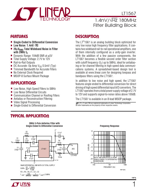
121567faTotal Supply Voltage (V + to V –)............................12.6V Input Current (Note 2)........................................±25mA Operating Temperature Range (Note 3)LT1567C..............................................–40°C to 85°C LT1567I...............................................–40°C to 85°C Specified Temperature Range (Note 4)LT1567C..............................................–40°C to 85°C LT1567I...............................................–40°C to 85°C Storage Temperature Range.................–65°C to 150°C Lead Temperature (Soldering, 10 sec)..................300°CORDER PART NUMBER MS8 PART MARKINGT JMAX = 150°C, θJA = 200°C/WLTWH LTWJLT1567CMS8LT1567IMS8(Note 1)The ● denotes the specifications that apply over the full operating temperature range (Note 4), otherwise specifications and typical values are at T A = 25°C. V S = ±2.5V, R L = 1K, V OUT = 0 on both amplifiers unless otherwise noted.PARAMETER CONDITIONS MIN TYP MAX UNITSTotal Supply Voltage 2.712V Supply CurrentV S = ±1.5V ●8.515mA V S = ±2.5V ●916mA V S = ±5V●1119mA OA Output Positive Voltage SwingV S = ±1.5V, R L = 1k ● 1.30 1.45V V S = ±2.5V, R L = 1k ● 2.20 2.45V V S = ±2.5V, R L =100● 1.90 2.25V V S = ±5V, R L = 1k ● 4.70 4.90V OA Output Negative Voltage SwingV S = ±1.5V, R L = 1k ●–1.30–1.45V V S = ±2.5V, R L = 1k ●–2.20–2.45V V S = ±2.5V, R L =100●–2.00–2.30V V S = ±5V, R L = 1k●–4.70–4.90V INV Output Positive Voltage SwingV S = ±1.5V, R L = 1k ● 1.30 1.40V V S = ±2.5V, R L = 1k● 2.20 2.50V V S = ±2.5V, R L = 100 (LT1567I Only, Note 5)● 1.80 2.00V V S = ±5V, R L = 1k● 4.60 4.80V INV Output Negative Voltage SwingV S = ±1.5V, R L = 1k ●–1.30–1.40V V S = ±2.5V, R L = 1k●–2.20–2.40V V S = ±2.5V, R L = 100 (LT1567I Only, Note 5)●–1.80–2.00V V S = ±5V, R L = 1k●–4.50–4.80VCommon Mode Input Voltage Range (DC BIAS, Pin 5)V S = ±1.5V, CMRR ≥ 40dB (Note 6)●–0.50.5V (See Pin Functions)V S = ±5V, CMRR ≥ 40dB (Note 6)●–3.8 3.5V DC Common Mode Rejection Ratio (CMRR)V S = ±1.5V, DC BIAS = –0.25V to 0.25V ●80dB V S = ±5V, DC BIAS = –2.5V to 2.5V ●6590dB DC Power Supply Rejection Ratio (PSRR)V S = ±1.5V to ±5V, DC BIAS = 0V●80100dB OA Input Offset Voltage ●0.53mV INV Output Offset Voltage●59mVConsult LTC Marketing for parts specified with wider operating temperature ranges.1234OAOUT OAIN BYPASSV –8765V +INVOUT INVIN DC BIASTOP VIEWMS8 PACKAGE 8-LEAD PLASTIC MSOP ABSOLUTE AXI U RATI GSW W WU PACKAGE/ORDER I FOR ATIOUUW ELECTRICAL CHARACTERISTICSOrder Options Tape and Reel: Add #TRLead Free: Add #PBF Lead Free Tape and Reel: Add #TRPBF Lead Free Part Marking: /leadfree/31567faNote 1: Stresses beyond those listed under Absolute Maximum Ratings may cause permanent damage to the device. Exposure to any Absolute Maximum Rating condition for extended periods may affect device reliability and lifetime.Note 2: The inputs of each op amp are protected by back-to-back diodes and diodes to each supply. If either input exceeds the supply or thedifferential input voltage exceeds 1.4V, the input current should be limited to less than 25mA.Note 3: The LT1567C and LT1567I are guaranteed functional over the operating temperature range –40°C to 85°C.Note 4: The LT1567C is guaranteed to meet specified performance from 0°C to 70°C. The LT1567C is designed, characterized and expected to meet specified performance from –40°C to 85°C but not tested or QA sampled at these temperatures. The LT1567I is guaranteed to meet specified performance from –40°C to 85°C.PARAMETER CONDITIONSMIN TYP MAX UNITS OA Input Bias Current ●310µA DC BIAS Input Bias Current ●615µA OA DC Open-Loop GainV S = ±1.5V, R L = 1k, V O = –1V to 1V ●7.555V/mV V S = ±2.5V, R L = 1k, V O = –2V to 2V●1060V/mV V S = ±2.5V, R L = 100, V O = –1.5V to 1.5V ● 1.27.0V/mV V S = ±5V, R L = 1k, V O = –4V to 4V ●1080V/mVINV DC GainV S = ±1.5V, R L = 1k, V IN = –1V to 1V ●0.97 1.04V/V V S = ±2.5V, R L = 1k, V IN = –2V to 2V ●0.97 1.04V/V V S = ±2.5V, R L = 100, V IN = –1.5V to 1.5V ●0.97 1.04V/V V S = ±5V, R L = 1k, V IN = –4V to 4V ●0.97 1.04V/V INV DC Input Resistance V S = ±2.5V, R L = 1k, V IN = –2V to 2V ●450600750ΩOA Gain Bandwidth ProductMeasured at 2MHz, V S = ±1.5V ●100180MHz Measured at 2MHz, V S = ±2.5V ●110185MHz Measured at 2MHz, V S = ±5V ●120190MHz INV Bandwidth –3dB85MHz INV AC Gain Measured at 2MHz ●0.961.0 1.05V/V OA Slew Rate V S = ±5V 55V/µs INV Slew RateV S = ±5V 90V/µs OA Input Voltage Noise Density (Note 7) f = 100kHz 1.4nV/√Hz OA Input Current Noise Densityf = 100kHz1.0pA/√Hz Wideband Output Noise for a Second Order Filter (Figure 1)f C = 2MHz, BW = 4MHz (Note 8)20µV RMS f C = 5MHz, BW = 10MHz (Note 8)30µV RMSTotal Harmonic Distortion (THD) f = 1MHz, f C = 2MHz, V OUT = 1V RMS –88dB for a Second Order Filter (Figure 1) f = 2.5MHz, f C = 5MHz, V OUT = 1V RMS–70dB Output Short-Circuit Current (Note 9)●850mA OA Output Impedance f = 100kHz, OA Connected as 0.03ΩUnity-Gain Inverter INV Output Impedancef = 100kHz0.7ΩNote 5: With INVIN pin driven to ±2V.Note 6: This parameter is not 100% tested.Note 7: The input referred voltage noise density of the unity gain inverter is 5.6nV/√Hz which includes the noise of the gain setting resistors.Note 8: For f C = 2MHz, C1 = C2 = 180pF, R1 = R2 = 604Ω, R3 = 316Ω and for f C = 5MHz, C1 = C2 = 180pF, R1 = R2 = 232Ω, R1 = 130Ω. BW is the bandwidth of the noise measurement (Figure 1 circuit).Note 9: Under direct short circuit conditions, with T A < 25°C the output current is reduced.ELECTRICAL CHARACTERISTICSThe ● denotes the specifications that apply over the full operating temperature range (Note 4), otherwise specifications and typical values are at T A = 25°C. V S = ±2.5V, R L = 1K, V OUT = 0 on both amplifiers unless otherwise noted.4561567faOAOUT (Pin 1): Output of the Uncommitted Op Amp (OA).As with most wideband op amps, it is important to avoid connecting heavy capacitive loads (above about 10pF )directly to this output. Such loads will impair AC stability and should be isolated from the output through series resistance.OAIN (Pin 2): Inverting or “–” Input of the Uncommitted Op Amp (OA) in the LT1567. The noninverting or “+” input of this amplifier is shared with that of the INV amplifier and accessed via the DC BIAS and BYPASS pins. The OA amplifier is optimized for minimal wideband noise.BYPASS (Pin 3): AC Ground Bypass. A decoupling capaci-tor, typically 0.1µF, from this pin to a printed circuit ground plane must be used. Use the shortest possible wiring.Power Supply Pins (Pins 4, 8): The V – and V + pins should be bypassed with 0.1µF capacitors to an adequate analog ground plane using the shortest possible wiring. Electri-cally clean supplies and a low impedance ground are important to obtain the wide dynamic range and band-width available from the LT1567. Low noise linear power supplies are recommended. Switching supplies require special care because of the inevitable risk of their switch-ing noise coupling into the signal path, reducing dynamic range.DC BIAS (Pin 5): DC Biasing Input. Sets the DC voltage at the noninverting inputs of the two internal amplifiers;designed for use as a DC reference, not a signal input.The DC BIAS input includes a small series resistor, both to balance DC offsets in the presence of input bias currents and also to suppress the “Q” factor of possible parasitic high frequency resonant circuits introduced by wiring inductance. The reference voltage at the noninverting inputs of the two amplifiers is decoupled for very high frequencies with a small internal capacitor to the chip substrate, nominally 7pF. An external capacitor, typically 0.1µF, to a nearby ground plane must be added at Pin 3(BYPASS) for a clean wideband DC reference biasing voltage.INVIN (Pin 6): Unity-Gain Inverter Input. The “inverter”(INV) amplifier in the LT1567 is connected to internal resistors (nominally 600Ω each) to form a closed-loop amplifier with a wideband voltage gain of nominally –1.This amplifier is similar to the uncommitted op amp (OA)but is optimized for high frequency linearity.INVOUT (Pin 7): Output of the INV or “Inverter” Amplifier,with a Nominal Gain of –1 from the INVIN Pin. As with most wideband op amps, it is important to avoid connect-ing heavy capacitive loads (above about 10pF) directly to this output. Such loads will impair AC stability and should be isolated from the output through series resistance.PI FU CTIO SU U U789101567faAPPLICATIO S I FOR ATIOW UUU output from the INV block (Pin 7). These two outputs maintain equal gain and 180º phase shift over a wide frequency range. This feature permits choosing the signal polarity in single ended applications, and also performs single ended to differential conversion. The latter property is useful as an antialiasing filter to drive standard mono-lithic A/D converters having differential inputs, as illus-trated on the first page of this data sheet.Dealing with High Source ImpedancesThe voltage V IN in Figure 1, on the left side of R1, is the signal voltage that the filter sees. If a voltage source with significant internal impedance drives the V IN node in F igure 1, then the filter input V IN may differ from the source’s open-circuit output, and the difference can be complex, because the filter presents a complex imped-ance to V IN . A rule of thumb is that a source impedance is negligibly “low” if it is much smaller than R1 at frequencies of interest. Otherwise, the source impedance (resistive or reactive) effectively adds to R1 and may change the signal frequency response compared to that with a low source impedance. If the source is resistive and predictable, then it may be possible to design for it by reducing R1.Unpredictable or nonresistive source impedances that are not much less than R1 should be buffered.Construction and Instrumentation CautionsElectrically clean construction is important in applica-tions seeking the full dynamic range and bandwidth of the LT1567. Using the shortest possible wiring or printed-circuit paths will minimize parasitic capacitance and inductance. High quality supply bypass capacitors of 0.1µF near the chip, connected to a ground plane, provide good decoupling from a clean, low inductance power source. But several inches of wire (i.e., a few microhenrys of inductance) from the power supplies, unless decoupled by substantial capacitance (≥10µF ) near the chip, cancause a high Q LC resonance in the hundreds of kHz in the chip’s supplies or ground reference. This may impair filter performance at those frequencies. In stringent filter applications, a compact, carefully laid out printed circuit board with good ground plane makes a difference in both stopband rejection and distortion. Finally, equipment to measure filter performance can itself introduce distortion or noise. Checking for these limits with a wire in place of the filter is a prudent routine procedure.Low Noise Differential CircuitsThe LT1567 is an optimum analog building for designing single supply differential circuits to process low level signals. F igure 3 shows a single ended to differential amplifier driving a 1st order differential RC filter. The differential output of Figure 3 is a function of input (V IN )and the V REF voltage on Pin 5. (The range of the V REF voltage on Pin 5 in Figures 3, 4 and 5 is the common mode input voltage range parameter under Electrical Characteristics.)The graph of Figure 3 shows the differen-tial signal-to-noise ratio for a gain of 2 and a gain of 10.Increasing the differential gain increases the differential signal-to-noise ratio. The equivalent input noise is equal to the output noise divided by the gain. For example, with a gain equal to 2 (R2 = R1 = 200Ω) and a gain equal to 10(R2 = 1k, R1 = 200Ω), the equivalent input noise is 4.59nV/√Hz and 2.04nV/√Hz respectively. The V REF voltage on Pin 5 can be set by a voltage divider or a reference voltage source. To maximize the unclipped LT1567 output swing,the DC output voltage should be set at V +/2. However, if V INDC (the input DC voltage) is within the range of V REF ,then V REF can be equal to V INDC . The input signal can also be AC coupled to the input resistor, R1, and V REF set to the DC voltage of the circuit following the amplifier. F or example, V REF might be set to 1.2V to bias the input of an I and Q modulator used in broadband communication systems.1112131415Information furnished by Linear Technology Corporation is believed to be accurate and reliable.However, no responsibility is assumed for its use. Linear Technology Corporation makes no represen-tation that the interconnection of its circuits as described herein will not infringe on existing patent rights.16Linear Technology Corporation1630 McCarthy Blvd., Milpitas, CA 95035-7417(408) 432-1900 ● FAX: (408) 434-0507 ● © LINEAR TECHNOLOGY CORPORA TION 2001LT 0406 REV A • PRINTED IN USA。
Luat 4G LTE 模块 AT 命令手册说明书

Luat4G LTE模块AT命令手册V5.0.8适用模块:Air720/Air724系列发布时间:2022/01/14修改记录2021.09.27定义NMEA解析朱先飞2021.09.27传入AGPS定位,所需的大概经纬度信息朱先飞2021.10.29短信特定字符触发RI功能AT*CMCRI目前朱先飞还不支持2021.12.13支持重新打开usb的指令王忠明2022.01.05主持查询ims注册状态的指令AT+CIREG陈旭东>=301848 V5.0.72022.06.23添加获取HTTP响应数据指令AT+HTTPGET陈旭东>=401853 2022.07.15添加cipsend的返回值的说明刘飞扬V5.0.82022.09.26添加EC618文档说明沈园园目录1AT命令概述 (13)2基本命令 (16)3配置命令 (23)4设备控制命令 (42)5网络服务相关命令 (66)5.30(URC)工程模式基本信息:+EEMGINFOBASIC (103)1.Non TD mode: (107)2.TD mode: (108)6通话控制和音频相关命令 (116)6.21(URC)IMS注册状态信息:+CIREGU (131)7短消息命令 (132)8电话本命令 (159)9分组域相关命令 (165)10NTP相关命令 (181)11文件系统读写命令 (183)12嵌入式TCPIP命令 (189)13IP应用相关命令 (239)14HTTP相关命令 (241)15FTP相关命令 (254)16MQTT相关命令 (277)17蓝牙相关命令 (290)18GPS相关的命令 (307)1AT命令概述 (13)1.1文档目的 (13)1.2惯例和术语缩写 (13)1.3AT命令语法 (14)1.4AT命令最大响应时间 (15)2基本命令 (16)2.1查询制造商名称:AT+CGMI (16)2.2查询模块型号:AT+CGMM (16)2.3查询模块版本信息:AT+CGMR (16)2.4查询IMEI号:AT+CGSN (17)2.5查询SIM卡ICCID号码:AT+CCID(/ICCID) (17)2.6查询IMSI:AT+CIMI (18)2.7查询产品信息:ATI (18)2.8查询模块FIRMWARE版本:AT+VER (19)2.9查询平台硬件版本:AT^HVER (19)2.10查询各种信息:AT*I (20)2.11重复上一条命令:A/ (21)2.12写SN号命令:AT+WISN (21)2.13重启模块:AT+RESET (22)3配置命令 (23)3.1选择TE字符集:AT+CSCS (23)3.2保存用户当前的配置:AT&W (24)3.3设置命令回显模式:ATE (24)3.4恢复所有参数为出厂配置:AT&F (24)3.5设置结果码抑制模式:ATQ (24)3.6设置TA响应内容的格式:ATV (25)3.7设置CONNECT结果码格式和监测呼叫进程:ATX (26)3.8设置自动应答前振铃次数:ATS0 (26)3.9FOTA空中升级:AT+UPGRADE (27)3.10设置指令行终止符:ATS3 (33)3.11设置命令行编辑字符:ATS5 (33)3.12设置CDC功能模式:AT&C (33)3.13设置DTR功能模式:AT&D (34)3.14实时时钟:AT+CCLK (34)3.15设置USB模式:AT+SETUSB (35)3.16设备错误:AT+CMEE (36)3.17错误码描述:+CME ERROR:<ERR> (36)4设备控制命令 (42)4.1手机活动状态:AT+CPAS (42)4.2模块功能模式:AT+CFUN (43)4.3关机:AT+CPOWD (44)4.4输入PIN码:AT+CPIN (44)4.5设备锁定:AT+CLCK (45)4.6修改密码:AT+CPWD (46)4.7网络灯闪烁的时间间隔:AT+SLEDS (47)4.8设置TE-TA波特率:AT+IPR (48)4.9设置TE-TA帧格式:AT+ICF (49)4.10设置指令行换行字符:ATS4 (50)4.11TE-TA本地流量控制:AT+IFC (51)4.12多路复用:AT+CMUX (52)4.13开启和关闭SIM卡在位硬件检测:AT+CSDT (53)4.14检测某个插槽的SIM卡是否在位:AT*SIMDETEC (53)4.15控制S IM卡状态主动上报:AT^CARDMODE (54)4.16获取S IM类型:AT*EUICC (55)4.17通过UART口设置睡眠唤醒:AT+CSCLK (55)4.18设置睡眠等待时间:AT+WAKETIM (57)4.19设置RI指示功能:AT+CFGRI (58)4.20短信特定字符触发RI功能:AT*CMCRI (59)4.21设置MAC地址:AT+MIFIMAC (59)4.22读取ADC:AT+CADC (60)4.23读取VBAT电压:AT+CBC (60)4.24打开/关闭网络灯:AT+CNETLIGHT (61)4.26SIM卡自动切换开关:AT*SIMAUTO (64)4.27RNDIS/ECM功能开关:AT+RNDISCALL (64)4.28SECURE BOOT使能开关:AT*SECUREBOOT (64)4.29重新打开USB:AT+SYSNV=1,”UREBOOT”,1 (65)5网络服务相关命令 (66)5.1查询信号质量:AT+CSQ (66)5.2查询信号质量(扩展):AT+CESQ (67)5.3打开CSQ主动上报:AT*CSQ (68)5.4网络注册信息:AT+CREG (69)5.5E-UTRAN EPS网络注册状态:AT+CEREG (71)5.6设置网络模式:AT^SYSCONFIG (72)5.7查询CID相关的上下文定义:AT+CGCONTRDP (73)5.8运营商查询和选择:AT+COPS (75)5.9自动时区更新:AT+CTZU (77)5.10打开NITZ自动上报:AT+CTZR (77)5.11(URC)NITZ自动上报:+NITZ:<TIME>,<DS> (77)5.12设置小区背景搜寻:AT+BGLTEPLMN (78)5.13使能HSDPA和HSUPA:AT*EHSDPA (79)5.14GSM/UMTS/LTE模式和频段设置:AT*BAND (81)5.15查询当前工作频段:AT*BANDIND (84)5.16查询接入机制(A CCESS T ECHNOLOGY):AT^CACAP (88)5.17查询当前的系统信息:AT^SYSINFO (88)5.18设置无线接入方式:AT+CTEC (90)5.19小区/频率锁:AT*CELL (90)5.20读取基站定位(LBS)信息和时间:AT+CIPGSMLOC (92)5.21读取WIFI定位信息和时间:AT+WIFILOC (94)5.22获取WIFI信息:AT+WIFISCAN (96)5.23流量查询命令:AT^DATAINFO (96)5.24(URC)手动PLMN选择选项:+MSRI (97)5.25(URC)系统模式:^MODE (97)5.26(URC)SIM卡状态上报:^SIMST (98)5.27小区信息查询:AT+CCED (98)5.28设置工程模式:AT+EEMOPT (101)5.29在工程模式下查询GSM/UMTS/LTE信息:AT+EEMGINFO (102)5.30(URC)工程模式基本信息:+EEMGINFOBASIC (103)5.31(URC)GSM工程模式下当前小区的信息:+EEMGINFOSVC (103)5.32(URC)GSM工程模式下PS信息:+EEMGINFOPS (104)5.33(URC)GSM工程模式下邻接小区的信息:+EEMGINFONC (105)5.34(URC)工程模式下当前网络状态:+EEMGINBFTM (106)5.35(URC)UMTS工程模式下当前小区的信息:+EEMUMTSSVC (106)5.36(URC)UMTS工程欧式下同频率信息:+EEMUMTSINTRA (110)5.37(URC)UMTS工程模式下频间信息:+EEMUMTSINTER (110)5.38(URC)UMTS工程模式下无线接入技术间信息:+EEMUMTSINTERRAT (111)5.39(URC)LTE工程模式下服务小区信息:+EEMLTESVC (111)5.41(URC)LTE工程模式下频间信息:+EEMLTEINTER (113)5.42(URC)LTE工程模式下无线接入技术间信息:+EEMLTEINTERRAT (113)5.43(URC)事件控制指示:+CIEV (114)5.44(URC)网络服务类型指示 (115)6通话控制和音频相关命令 (116)6.1打开VOLTE功能:AT+SETVOLTE (116)6.2发起呼叫:ATD (116)6.3接听来电:ATA (117)6.4挂断通话:ATH (118)6.5挂断通话:AT+CHUP (118)6.6列出所有当前的呼叫:AT+CLCC (118)6.7设置主叫号码显示:AT+CLIP (120)6.8呼叫保持和多方通话:AT+CHLD (121)6.9产生DTMF音:AT+VTS (122)6.10DTMF TONE周期:AT+VTD (123)6.11TTS(T EXT T O S PEECH)功能:AT+CTTS (123)6.12设置TTS播放模式:AT+CTTSPARAM (124)6.13音频录制:AT+CAUDREC (124)6.14语音文件播放:AT+CAUDPLAY (125)6.15语音通道切换:AT+AUDCH (127)6.16通话音量控制:AT+CLVL (128)6.17本地音频播放音量控制:AT+CRSL (128)6.18音频功放类型设置指令:AT+SPKPA (129)6.19音频MIC增益设置指令:AT+CACCP (129)6.20IMS注册状态指令:AT+CIREG (130)6.21(URC)IMS注册状态信息:+CIREGU (131)7短消息命令 (132)7.1PDU短信编码格式介绍 (132)7.2选择短消息服务:AT+CSMS (134)7.3短消息优先存储区选择:AT+CPMS (134)7.4短消息中心地址:AT+CSCA (136)7.5短消息格式:AT+CMGF (136)7.6设置短信TEXT模式参数:AT+CSMP (137)7.7控制TEXT模式下短信头信息显示:AT+CSDH (138)7.8新消息指示:AT+CNMI (140)7.9新短消息确认:AT+CNMA (142)7.10发送短信:AT+CMGS (143)7.11把消息写入存储器:AT+CMGW (145)7.12从存储器发送短信:AT+CMSS (147)7.13短信链路控制命令:AT+CMMS (148)7.14读短信:AT+CMGR (149)7.15列举短消息:AT+CMGL (151)7.16删除短消息:AT+CMGD (153)7.18短信业务失败结果码:CMS ERROR:<ERR> (155)8电话本命令 (159)8.1选择电话本存储类型:AT+CPBS (159)8.2读取电话本记录:AT+CPBR (160)8.3查找电话本记录:AT+CPBF (161)8.4写电话本记录:AT+CPBW (162)8.5本机号码:AT+CNUM (164)9分组域相关命令 (165)9.1GPRS网络注册状态:AT+CGREG (165)9.2GPRS附着分离:AT+CGATT (166)9.3PDP上下文定义:AT+CGDCONT (167)9.4PDP上下文鉴权参数:AT+CGAUTH (169)9.5显示PDP地址:AT+CGPADDR (169)9.6PDP上下文激活:AT+CGACT (170)9.7可接受的最小服务质量简报:AT+CGQMIN (171)9.8请求的服务质量简报:AT+CGQREQ (172)9.9控制非请求GPRS事件上报:AT+CGEREP (173)9.10(URC)分组域事件URC上报:+CGEV (174)9.11通过CID查询本地IP地址:AT*GETIP (177)9.12打开或关闭自动获取APN:AT+AUTOAPN (177)9.13设置LTE下缺省的PDP承载:AT*CGDFLT (178)9.14设置LTE缺省的PDP承载的鉴权参数:AT*CGDFAUTH (179)10NTP相关命令 (181)10.1设置GPRS承载场景ID:AT+CNTPCID (181)10.2同步网络时间:AT+CNTP (181)11文件系统读写命令 (183)11.1创建一个文件:AT+FSCREATE (183)11.2读文件:AT+FSREAD (183)11.3写文件:AT+FSWRITE (184)11.4获取盘符:AT+FSDRIVE (184)11.5显示文件目录列表:AT+FSLS (185)11.6获取可用空间大小:AT+FSMEM (185)11.7创建目录:AT+FSMKDIR (185)11.8删除目录:AT+FSRMDIR (186)11.9删除文件:AT+FSDEL (186)11.10获取文件大小:AT+FSFLSIZE (186)11.11使用方法举例 (187)12嵌入式TCPIP命令 (189)12.1启动多IP连接:AT+CIPMUX (189)12.2启动任务并设置接入点APN、用户名、密码:AT+CSTT (189)12.3专网卡设置APN、用户名、密码和鉴权方式:AT+CPNETAPN (190)12.4激活移动场景(或发起GPRS或CSD无线连接):AT+CIICR (191)12.5查询本地IP地址:AT+CIFSR (191)12.6设置TCP使用SSL功能:AT+CIPSSL (192)12.7配置TCP SSL参数:AT+SSLCFG (192)12.8配置本地TCP端口:AT+CLPORT (196)12.9建立TCP连接或注册UDP端口号:AT+CIPSTART (197)12.10选择TCPIP应用模式:AT+CIPMODE (199)12.11选择非透传数据发送模式:AT+CIPQSEND (199)12.12设置接收的数据末尾是否自动添加回车换行:AT+CIPRXF (200)12.13配置透明传输模式:AT+CIPCCFG (200)12.14发送数据:AT+CIPSEND (201)12.15设置自动发送数据前的定时时间:AT+CIPATS (203)12.16设置发送数据时是否显示‘>’和发送情况提示:AT+CIPSPRT (203)12.17查询当前连接状态:AT+CIPSTATUS (204)12.18查询已连接数据传输状态:AT+CIPACK (205)12.19设置为CSD或GPRS连接模式:AT+CIPCSGP (206)12.20配置域名服务器DNS:AT+CDNSCFG (206)12.21域名解析:AT+CDNSGIP (208)12.22设置单链接接收数据时是否显示发送方的IP地址和端口号:AT+CIPSRIP (209)12.23设置单链接接收数据是否显示IP头:AT+CIPHEAD (209)12.24设置单链接接收数据是否在IP头显示传输协议:AT+CIPSHOWTP (209)12.25配置TCP协议的参数:AT+TCPUSERPARAM (210)12.26多链接时接收数据:+RECEIVE (211)12.27保存TCPIP应用上下文:AT+CIPSCONT (211)12.28手动获得网络数据:AT+CIPRXGET (212)12.29关闭TCP或UDP连接:AT+CIPCLOSE (215)12.30关闭移动场景:AT+CIPSHUT (215)12.31修改RNDIS网卡网关IP地址:AT+ROUTEIP (216)12.32P ING回声请求命令:AT+CIPPING (216)12.33设置TCP保活(KEEP-ALIVE)参数:AT+CIPTKA (217)12.34心跳包参数设置:AT^HEARTCONFIG (218)12.35设置心跳包内容:AT^HEARTBEAT (219)12.36设置HEX编码格式心跳包内容:AT^HEARTBEATHEX (220)12.37查询心跳包发送情况:AT^HEARTINQUIRE (221)12.38从数据模式或PPP在线模式切换至命令模式:+++ (222)12.39从命令模式切换至数据模式:ATO (223)12.40TCP/UDP错误码 (223)12.41状态机 (224)12.42模块上电初始化以及TCPIP流程 (226)12.43使用方法举例 (228)13IP应用相关命令 (239)13.1IP应用设置:AT+SAPBR (239)14HTTP相关命令 (241)14.2启用SSL:AT+HTTPSSL (241)14.3设置HTTP参数值:AT+HTTPPARA (241)14.4写数据:AT+HTTPDATA (243)14.5HTTP方式激活:AT+HTTPACTION (244)14.6查询HTTP服务响应:AT+HTTPREAD (245)14.7获取HTTP服务响应数据:AT+HTTPGET (246)14.8查询HTTP头信息:AT+HTTPHEAD (246)14.9保存HTTP应用上下文:AT+HTTPSCONT (247)14.10终止HTTP任务:AT+HTTPTERM (247)14.11HTTP错误码:ERROR:<ERR CODE> (248)14.12使用方法举例 (248)15FTP相关命令 (254)15.1设置FTP控制端口:AT+FTPPORT (254)15.2设置FTP主动或被动模式:AT+FTPMODE (254)15.3设置FTP数据传输类型:AT+FTPTYPE (254)15.4设置FTP输入类型:AT+FTPPUTOPT (255)15.5设置FTP承载标识:AT+FTPCID (255)15.6设置FTP下载续传:AT+FTPREST (256)15.7设置FTP服务器地址:AT+FTPSERV (256)15.8设置FTP用户名称:AT+FTPUN (256)15.9设置FTP密码:AT+FTPPW (257)15.10设置FTP下载文件名称:AT+FTPGETNAME (257)15.11设置FTP下载文件路径:AT+FTPGETPATH (257)15.12设置FTP上传文件名称:AT+FTPPUTNAME (258)15.13设置FTP上传文件路径:AT+FTPPUTPATH (258)15.14远程服务器上创建文件目录:AT+FTPMKD (259)15.15远程服务器上删除文件目录:AT+FTPRMD (259)15.16下载文件:AT+FTPGET (260)15.17上传文件:AT+FTPPUT (261)15.18下载文件(扩展):AT+FTPEXTGET (261)15.19上传文件(扩展):AT+FTPEXTPUT (262)15.20下载文件并保存到文件系统中:AT+FTPGETTOFS (263)15.21从文件系统上传文件到服务器:AT+FTPPUTFRMFS (264)15.22从文件系统加载到RAM中并用FTPPUT上传:AT+FTPFILEPUT (264)15.23获取远程服务器上文件目录:AT+FTPLIST (265)15.24获取远程服务器上文件大小:AT+FTPSIZE (266)15.25获取FTP状态:AT+FTPSTATE (266)15.26保存FTP应用上下文:AT+FTPSCONT (266)15.27删除服务器上指定的文件:AT+FTPDELE (267)15.28退出当前FTP会话:AT+FTPQUIT (267)15.29使用方法举例 (267)16MQTT相关命令 (277)16.1设置MQTT相关参数:AT+MCONFIG (277)16.3客户端向服务器请求会话连接:AT+MCONNECT (278)16.4发布消息:AT+MPUB (279)16.5发布定长消息:AT+MPUBEX (280)16.6订阅主题:AT+MSUB (281)16.7取消订阅主题:AT+MUNSUB (282)16.8打印收到的所有的订阅消息:AT+MQTTMSGGET (283)16.9设置订阅消息的打印模式:AT+MQTTMSGSET (283)16.10MQTT消息编码格式切换:AT+MQTTMODE (284)16.11关闭TCP连接:AT+MIPCLOSE (285)16.12关闭MQTT连接:AT+MDISCONNECT (285)16.13查询MQTT连接状态:AT+MQTTSTATU (285)16.14使用方法举例 (285)17蓝牙相关命令 (290)17.1蓝牙开关:AT+BTCOMM=ENABLE (290)17.2设置名称:AT+BLECOMM=NAME (290)17.3设置广播数据:AT+BLEADV=ADVDATA (291)17.4设置响应数据:AT+BLEADV=SCANRSPDATA (291)17.5设置广播参数:AT+BLEADV=ADVPARAM (292)17.6添加服务:AT+BLEADV=ADDSERVICE (293)17.7添加特征:AT+BLEADV=ADDCHARACTERISTIC (294)17.8添加描述:AT+BLEADV=ADDDESCRIPTOR (295)17.9清除所有自定义服务:AT+BLEADV=CLEANALLSERVICE (295)17.10添加白名单:AT+BLECOMM=ADDWHITELIST (296)17.11移除白名单:AT+BLECOMM=REMOVEWHITELIST (296)17.12清空白名单:AT+BLECOMM=CLEANWHITELIST (296)17.13设置BEACON数据:AT+BLEADV=BEACONDATA (296)17.14广播开关:AT+BLEADV=ENABLE (297)17.15(URC)连接状态上报:+BLEIND=CONNECT (297)17.16(URC)断开状态上报:+BLEIND=DISCONNECT (298)17.17设置扫描参数:AT+BLESCAN=SCANPARAM (298)17.18扫描开关:AT+BLESCAN=ENABLE (299)17.19(URC)扫描结果上报:+BLEIND=SCAN (299)17.20连接从设备:AT+BLECOMM=CONNECT (300)17.21断开从设备:AT+BLECOMM=DISCONNECT (300)17.22发现服务UUID:AT+BLECOMM=FINDSERVICE (300)17.23(URC)服务UUID上报:+BLEIND=FINDSERVICE (301)17.24发现服务内的特征:AT+BLECOMM=FINDCHARACTERISTIC (301)17.25(URC)特征UUID上报:+BLEIND=FINDCHARACTERISTIC (302)17.26通知开关:AT+BLECOMM=NOTIFICATION (302)17.27发送数据:AT+BLECOMM=SENDDATA (302)17.28(URC)接收数据上报:+BLEIND=DATA (303)17.29蓝牙MAC地址:AT+BTMAC (303)17.30使用方法举例 (304)18GPS相关的命令 (307)18.1GPS开关:AT+CGNSPWR (307)18.2读取GNSS信息:AT+CGNSINF (307)18.3打开GNSS URC上报:AT+CGNSURC (308)18.4将读取到的GNSS数据发送到AT口:AT+CGNSTST (309)18.5给GNSS发送控制命令:AT+CGNSCMD (309)18.6读取GNSS版本:AT+CGNSVER (310)18.7设置辅助定位:AT+CGNSAID (310)18.8删除EPO文件:AT+CGNSDEL (311)18.9增加VIB电压输出:AT+LDO (311)18.10定义NMEA解析:AT+CGNSSEQ (311)18.11传入AGPS定位,所需的大概经纬度信息:AT+CRFLOC (312)18.12检查EPO文件属性:AT+CGNSCHK (312)18.13使用方法举例 (313)1AT命令概述1.1文档目的本手册详细介绍了合宙Luat LTE模块做支持的AT命令集。
- 1、下载文档前请自行甄别文档内容的完整性,平台不提供额外的编辑、内容补充、找答案等附加服务。
- 2、"仅部分预览"的文档,不可在线预览部分如存在完整性等问题,可反馈申请退款(可完整预览的文档不适用该条件!)。
- 3、如文档侵犯您的权益,请联系客服反馈,我们会尽快为您处理(人工客服工作时间:9:00-18:30)。
100µs/DIV6011 TA0312ELECTRICAL CHARACTERISTICSThe ● denotes the specifications which apply over the full operating temperature range, otherwise specifications are at T A = 25°C. V S = 5V, 0V; V CM = 2.5V; R L to 0V; unless otherwise specified. (Note 5) SYMBOL PARAMETER CONDITIONS MIN TYP MAX UNITS V OS Input Offset Voltage (Note 8)LT6011AS8, LT6012AS2060µVT A = 0°C to 70°C●85µVT A = –40°C to 85°C●110µVLT6011ADD, LT6012AGN2585µVT A = 0°C to 70°C●135µVT A = –40°C to 85°C●170µVLT6011S8, LT6012S2575µVT A = 0°C to 70°C●100µVT A = –40°C to 85°C●125µVLT6011DD, LT6012GN, LT6011MS830125µVT A = 0°C to 70°C●175µVT A = –40°C to 85°C●210µV ∆V OS/∆T Input Offset Voltage Drift (Note 6)LT6011AS8, LT6011S8, LT6012AS,LT6012S●0.20.8µV/°CLT6011ADD,LT6011DD, LT6012AGN,LT6012GN, LT6011MS8●0.2 1.2µV/°C I OS Input Offset Current (Note 8)LT6011AS8, LT6011ADD, LT6012AS,LT6012AGN20300pAT A = 0°C to 70°C●450pAT A = –40°C to 85°C●600pALT6011S8, LT6011DD, LT6012S,LT6012GN, LT6011MS8150900pAT A = 0°C to 70°C●1200pAT A = –40°C to 85°C●1500pA I B Input Bias Current (Note 8)LT6011AS8, LT6011ADD, LT6012AS,LT6012AGN20±300pAT A = 0°C to 70°C●±450pAT A = –40°C to 85°C●±600pALT6011S8, LT6011DD, LT6012S,LT6012GN, LT6011MS8150±900pAT A = 0°C to 70°C●±1200pAT A = –40°C to 85°C●±1500pA Input Noise Voltage0.1Hz to 10Hz400nV P-P e n Input Noise Voltage Density f = 1kHz14nV/√Hz i n Input Noise Current Density f = 1kHz, Unbalanced Source Resistance0.1pA/√Hz R IN Input Resistance Common Mode, V CM = 1V to 3.8V10120GΩDifferential20MΩC IN Input Capacitance4pF V CM Input Voltage Range (Positive)Guaranteed by CMRR● 3.84V Input Voltage Range (Negative)Guaranteed by CMRR●0.71V CMRR Common Mode Rejection Ratio V CM = 1V to 3.8V●107135dB Minimum Supply Voltage Guaranteed by PSRR● 2.4 2.7V PSRR Power Supply Rejection Ratio V S = 2.7V to 36V, V CM = 1/2V S●112135dB A VOL Large-Signal Voltage Gain R L = 10k, V OUT = 1V to 4V●3002000V/mVR L = 2k, V OUT = 1V to 4V●2502000V/mV Channel Separation V OUT = 1V to 4V●110140dB360112fbELECTRICAL CHARACTERISTICSThe ● denotes the specifications which apply over the full operating temperature range, otherwise specifications are at T A = 25°C. V S = 5V, 0V; V CM = 2.5V; R L to 0V; unless otherwise specified. (Note 5) SYMBOL PARAMETER CONDITIONS MIN TYP MAX UNITS V OUT Maximum Output Swing No Load, 50mV Overdrive3555mV (Positive, Referred to V+)●65mVI SOURCE = 1mA, 50mV Overdrive120170mV●220mVMaximum Output Swing No Load, 50mV Overdrive4055mV(Negative, Referred to 0V)●65mVI SINK = 1mA, 50mV Overdrive150225mV●275mVI SC Output Short-Circuit Current (Note 3)V OUT = 0V, 1V Overdrive, Source1014mA●4mAV OUT = 5V, –1V Overdrive, Sink1021mA●4mA SR Slew Rate A V = –10, R F = 50k, R G = 5k0.060.09V/µsT A = 0°C to 70°C●0.05V/µsT A = –40°C to 85°C●0.04V/µs GBW Gain Bandwidth Product f = 10kHz250330kHz●225kHz t s Settling Time A V = –1, 0.01%, V OUT = 1.5V to 3.5V45µs t r, t f Rise Time, Fall Time A V = 1, 10% to 90%, 0.1V Step1µs ∆V OS Offset Voltage Match (Note 7)LT6011AS8, LT6012AS50120µVT A = 0°C to 70°C●170µVT A = –40°C to 85°C●220µVLT6011ADD, LT6012AGN50170µVT A = 0°C to 70°C●270µVT A = –40°C to 85°C●340µVLT6011S8, LT6012S50150µVT A = 0°C to 70°C●200µVT A = –40°C to 85°C●250µVLT6011DD, LT6012GN, LT6011MS860250µVT A = 0°C to 70°C●350µVT A = –40°C to 85°C●420µV ∆I B Input Bias Current Match (Note 7)LT6011AS8, LT6011ADD, LT6012AS,LT6012AGN50600pAT A = 0°C to 70°C●900pAT A = –40°C to 85°C●1200pALT6011S8, LT6011DD, LT6012S,LT6012GN, LT6011MS81800pAT A = 0°C to 70°C●2400pAT A = –40°C to 85°C●3000pA ∆CMRR Common Mode Rejection Ratio●101135dB Match (Note 7)∆PSRR Power Supply Rejection Ratio●106135dB Match (Note 7)I S Supply Current per Amplifier135150µAT A = 0°C to 70°C●190µAT A = –40°C to 85°C●210µA460112fbELECTRICAL CHARACTERISTICS The ● denotes the specifications which apply over the full operating temperature range, otherwise specifications are at T A = 25°C. V S = ±15V, V CM = 0V, R L to 0V, unless otherwise specified. (Note 5) SYMBOL PARAMETER CONDITIONS MIN TYP MAX UNITS V OS Input Offset Voltage (Note 8)LT6011AS8, LT6012AS30135µVT A = 0°C to 70°C●160µVT A = –40°C to 85°C●185µVLT6011ADD, LT6012AGN35160µVT A = 0°C to 70°C●210µVT A = –40°C to 85°C●225µVLT6011S8, LT6012S35150µVT A = 0°C to 70°C●175µVT A = –40°C to 85°C●200µVLT6011DD, LT6012GN, LT6011MS840200µVT A = 0°C to 70°C●250µVT A = –40°C to 85°C●275µV ∆V OS/∆T Input Offset Voltage Drift LT6011AS8, LT6011S8, LT6012AS, LT6012S●0.20.8µV/°C (Note 6)LT6011ADD, LT6011DD, LT6012AGN, LT6012GN, LT6011MS8●0.2 1.3µV/°C I OS Input Offset Current (Note 8)LT6011AS8, LT6011ADD, LT6012AS LT6012AGN20300pAT A = 0°C to 70°C●450pAT A = –40°C to 85°C●600pALT6011S8, LT6011DD, LT6012S, LT6012GN, LT6011MS8150900pAT A = 0°C to 70°C●1200pAT A = –40°C to 85°C●1500pA I B Input Bias Current (Note 8)LT6011AS8, LT6011ADD, LT6012AS, LT6012AGN20±300pAT A = 0°C to 70°C●±450pAT A = –40°C to 85°C●±600pALT6011S8, LT6011DD, LT6012S, LT6012GN, LT6011MS8150±900pAT A = 0°C to 70°C●±1200pAT A = –40°C to 85°C●±1500pA Input Noise Voltage0.1Hz to 10Hz400nV P-P e n Input Noise Voltage Density f = 1kHz13nV/√Hz i n Input Noise Current Density f = 1kHz, Unbalanced Source Resistance0.1pA/√Hz R IN Input Resistance Common Mode, V CM = ±13.5V50400GΩDifferential20MΩC IN Input Capacitance4pF V CM Input Voltage Range Guaranteed by CMRR●±13.5±14V CMRR Common Mode Rejection V CM = –13.5V to 13.5V115135dB Ratio●112135dB Minimum Supply Voltage Guaranteed by PSRR●±1.2±1.35V PSRR Power Supply Rejection Ratio V S = ±1.35V to ±18V●112135dBA VOL Large-Signal Voltage Gain R L = 10k, V OUT = –13.5V to 13.5V10002000V/mV●600V/mVR L = 5k, V OUT = –13.5V to 13.5V5001500V/mV●300V/mVChannel Separation V OUT = –13.5V to 13.5V●120140dB V OUT Maximum Output Swing No Load, 50mV Overdrive4580mV (Positive, Referred to V+)●100mVI SOURCE = 1mA, 50mV Overdrive140195mV●240mVMaximum Output Swing No Load, 50mV Overdrive4580mV (Negative, Referred to V–)●100mVI SINK = 1mA, 50mV Overdrive150250mV●300mV560112fb660112fbI SCOutput Short-Circuit Current V OUT = 0V, 1V Overdrive (Source)1015mA (Note 3)●5mA V OUT = 0V, –1V Overdrive (Sink)1020mA ●5mA SRSlew RateA V = –10, R F = 50k, R G = 5k 0.080.11V/µs T A = 0°C to 70°C ●0.07V/µs T A = –40°C to 85°C ●0.05V/µs GBW Gain Bandwidth Product f = 10kHz275350kHz ●250kHz t s Settling TimeA V = –1, 0.01%, V OUT = 0V to 10V 85µs t r , t f Rise Time, Fall TimeA V = 1, 10% to 90%, 0.1V Step 1µs ∆V OSOffset Voltage Match (Note 7)LT6011AS8, LT6012AS 50270µV T A = 0°C to 70°C ●320µV T A = –40°C to 85°C●370µV LT6011ADD, LT6012AGN 50320µV T A = 0°C to 70°C ●420µV T A = –40°C to 85°C ●450µV LT6011S8, LT6012S 70300µV T A = 0°C to 70°C ●350µV T A = –40°C to 85°C●400µV LT6011DD, LT6012GN, LT6011MS880400µV T A = 0°C to 70°C ●500µV T A = –40°C to 85°C●550µV ∆I BInput Bias Current Match (Note 7)LT6011AS8, LT6011ADD, LT6012AS, LT6012AGN 50600pA T A = 0°C to 70°C ●900pA T A = –40°C to 85°C●1200pA LT6011S8, LT6011DD, LT6012S, LT6012GN,LT6011MS81800pA T A = 0°C to 70°C ●2400pA T A = –40°C to 85°C●3000pA ∆CMRR Common Mode Rejection Ratio ●109135dB Match (Note 7)∆PSRR Power Supply Rejection Ratio ●106135dBMatch (Note 7)I SSupply Currentper Amplifier 260330µA T A = 0°C to 70°C ●380µA T A = –40°C to 85°C●400µAELECTRICAL CHARACTERISTICSThe ● denotes the specifications which apply over the full operatingtemperature range, otherwise specifications are at T A = 25°C. V S = ±15V, V CM = 0V, R L to 0V, unless otherwise specified. (Note 5)Note 1: Stresses beyond those listed under Absolute Maximum Ratings may cause permanent damage to the device. Exposure to any Absolute Maximum Rating condition for extended periods may affect device reliability and lifetime.Note 2: The inputs are protected by back-to-back diodes and internal series resistors. If the differential input voltage exceeds 10V, the input current must be limited to less than 10mA.Note 3: A heat sink may be required to keep the junction temperature below absolute maximum ratings.Note 4: Both the LT6011C/LT6012C and LT6011I/LT6012I are guaranteed functional over the operating temperature range of –40°C to 85°C.Note 5: The LT6011C/LT6012C are guaranteed to meet the specified performance from 0°C to 70°C and is designed, characterized and expected to meet specified performance from –40°C to 85°C but is not tested or QA sampled at these temperatures. The LT6011I/LT6012I are guaranteed to meet specified performance from –40°C to 85°C.Note 6: This parameter is not 100% tested.Note 7: Matching parameters are the difference between any two amplifiers. ∆CMRR and ∆PSRR are defined as follows: (1) CMRR and PSRR are measured in µV/V for the individual amplifiers. (2) The difference between matching amplifiers is calculated in µV/V. (3) The result is converted to dB.Note 8: The specifications for V OS , I B , and I OS depend on the grade and on the package. The following table clarifies the notations.SYMBOL PARAMETERCONDITIONSMIN TYP MAXUNITS STANDARD GRADEA GRADE S8 Package LT6011S8LT6011AS8DFN Package LT6011DD LT6011ADD S14 Package LT6012S LT6012AS GN16 Package LT6012GN LT6012AGN MS8 PackageLT6011MS8N/A760112fbTIME (SEC)0N O I S E V O L T A G E (0.2µV /D I V )86011 G092461071359V S = ±15V T A = 25°C8Output Saturation Voltage vs Load Current (Output Low)T A = 85°CV S = 5V, 0VTIME (SEC)N O I S E V O L T A G E (0.2µV /D I V )806011 G102040601007010305090V S = ±15V T A = 25°C91060112fbSmall-Signal Transient ResponseLarge-Signal Transient ResponseRail-to-Rail Output Swing20mV/DIVA V = 12µs/DIV6011 G282V/DIV A V = –150µs/DIV6011 G29V S = ±15V1V/DIVA V = –1100µs/DIV6011 G30V S = 5V, 0VTYPICAL PERFOR A CE CHARACTERISTICSU W0V 0VPreserving Input PrecisionPreserving the input accuracy of the LT6011/LT6012 re-quires that the applications circuit and PC board layout do not introduce errors comparable to or greater than the 25µV typical offset of the amplifiers. Temperature differentials across the input connections can generate thermocouple voltages of 10’s of microvolts so the connections to the input leads should be short, close together and away from heat dissipating components. Air currents across the board can also generate temperature differentials.The extremely low input bias currents (20pA typical) allow high accuracy to be maintained with high impedance sources and feedback resistors. The LT6011/LT6012 low input bias currents are obtained by a cancellation circuit on-chip. This causes the resulting I B + and I B – to be uncorrelated, as implied by the I OS specification being comparable to I B . Do not try to balance the input resistances in each input lead; instead keep the resistance at either input as low as possible for maximum accuracy.Leakage currents on the PC board can be higher than the input bias current. For example, 10G Ω of leakage between a 15V supply lead and an input lead will generate 1.5nA!Surround the input leads with a guard ring driven to the same potential as the input common mode to avoid exces-sive leakage in high impedance applications.Input ProtectionThe LT6011/LT6012 feature on-chip back-to-back diodes between the input devices, along with 500Ω resistors inseries with either input. This internal protection limits the input current to approximately 10mA (the maximum al-lowed) for a 10V differential input voltage. Use additional external series resistors to limit the input current to 10mA in applications where differential inputs of more than 10V are expected. For example, a 1k resistor in series with each input provides protection against 30V differential voltage.Input Common Mode RangeThe LT6011/LT6012 output is able to swing close to each power supply rail (rail-to-rail out), but the input stage is limited to operating between V – + 1V and V + – 1.2V. E xceed-ing this common mode range will cause the gain to drop to zero, however, no phase reversal will occur.Total Input NoiseThe LT6011/LT6012 amplifier contributes negligible noise to the system when driven by sensors (sources) with impedance between 20k Ω and 1M Ω. Throughout this range, total input noise is dominated by the 4kTR S noise of the source. If the source impedance is less than 20k Ω,the input voltage noise of the amplifier starts to contribute with a minimum noise of 14nV/√Hz for very low source im-pedance. If the source impedance is more than 1M Ω, the input current noise of the amplifier, multiplied by this high impedance, starts to contribute and eventually dominate.Total input noise spectral density can be calculated as:v e kTR i R n TOTAL n S n S ()()=++224APPLICATIO S I FOR ATIOWUU U 5V1112131415Information furnished by Linear Technology Corporation is believed to be accurate and reliable.However, no responsibility is assumed for its use. Linear Technology Corporation makes no represen-tation that the interconnection of its circuits as described herein will not infringe on existing patent rights.16Linear Technology Corporation1630 McCarthy Blvd., Milpitas, CA 95035-7417(408) 432-1900 ● FAX: (408) 434-0507 ● © LINEAR TECHNOLOGY CORPORA TION 2003LT 0406 REV B • PRINTED IN USA。