Yole LED Packaging Sample
AlInGaP II LED产品说明书
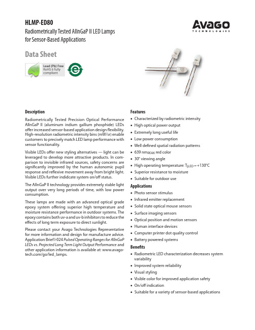
Features• Characterized by radiometric intensity • High optical power output • Extremely long useful life • Low power consumption• Well de ned spatial radiation patterns • 639 nm PEAK red color • 30° viewing angle• High operating temperature: T jLED = +130°C • Superior resistance to moisture • Suitable for outdoor useApplications• Photo sensor stimulus • Infrared emitter replacement • Solid state optical mouse sensors • Surface imaging sensors• Optical position and motion sensors • Human interface devices• Computer printer dot quality control • Battery powered systemsBene ts• Radiometric LED characterization decreases system variability• Improved system reliability • Visual styling• Visible color for improved application safety • On/o indication• Suitable for a variety of sensor-based applicationsDescriptionRadiometrically Tested Precision Optical Performance AlInGaP II (aluminum indium gallium phosphide) LEDs o er increased sensor-based application design exibility. High-resolution radiometric intensity bins (mW/sr) enable customers to precisely match LED lamp performance with sensor functionality.Visible LEDs o er new styling alternatives — light can be leveraged to develop more attractive products. In com-parison to invisible infrared sources, safety concerns are signi cantly improved by the human autonomic pupil response and re exive movement away from bright light. Visible LEDs further indidcate system on/o status.The AlInGaP II technology provides extremely stable light output over very long periods of time, with low power consumption.These lamps are made with an advanced optical grade epoxy system o ering superior high temperature and moisture resistance performance in outdoor systems. The epoxy contains both uv-a and uv-b inhibitors to reduce the e ects of long term exposure to direct sunlight.Please contact your Avago Technologies Representative for more information and design for manufacture advice. Application Brief I-024 Pulsed Operating Ranges for AlInGaP LEDs vs. Projected Long Term Light Output Performance and other application information is available at: /go/led_lamps.HLMP-ED80Radiometrically Tested AlInGaP II LED Lamps for Sensor-Based ApplicationsData SheetMinimum Radiometric Intensity Maximum Forward Voltage Part Number (mW/Sr) at 20 mA (V) at 20 mA HLMP-ED80-K0T00 7.2 2.6HLMP-ED80-K00007.22.4Device Selection GuidePackage DimensionsNOTE:ALL DIMENSIONS ARE IN mm (INCHES).(0.039)CATHODEFLATPart Numbering SystemH L M P-x x x x-x x x x xMechanical Option00: BulkV F Bin Selections0: Maximum V F 2.4 VT: Maximum V F 2.6 VMaximum Intensity Bin0: No maximum Iv bin limitMinimum Intensity BinRefer to device selection guideColorD: 630 nm redPackageE: T-1 3/4 (5 mm) round lamp Note: Please refer to AB 5337 for complete information on part numbering system.Absolute Maximum Ratings at T A = 25°CDC Forward Current [1,2,3].....................................................................................................50 mA Peak Pulsed Forward Current [2,3].......................................................................................100 mA Average Forward Current .......................................................................................................30 mA Reverse Voltage (I R = 100 µA) .........................................................................................................5 V LED Junction Temperature ........................................................................................................130°C Operating Temperature .........................................................................................–40°C to +100°C Storage Temperature ..............................................................................................–40°C to +100°C Notes:1. Derate linearly as shown in Figure 4.2. For long term performance with minimal light output degradation, drive currents between10 mA and 30 mA are recommended. For more information on recommended drive condi-tions, please refer to HP Application Brief I-024 (5966-3087E).3. Please contact your Avago sales representative about operating currents below 10 mA.Electrical/Optical Characteristics at T A = 25°CParameterSymbolMin.Typ.Max.UnitsTest ConditionsForward Voltage ED80-xx0xx V F 2.00 2.40 V I F = 20 mAED80-xxTxx 2.35 2.60Reverse Voltage V R 5 20 V I R = 100 µAPeak Wavelength λPEAK 639 nm Peak of Wavelength of SpectralDistribution at I F = 20 mA Dominant Wavelength [1] λd 630 nmSpectral Halfwidth ∆λ1/2 17 nm Wavelength Width at Spectral Distribution 1/2 Power Point atI F = 20 mASpeed of Response τs 20 ns Exponential Time Constant, e -t/τs Capacitance C 40 pF V F = 0, f = 1 MHzThermal Resistance R ΘJ-PIN240 °C/W LED Junction-to-Cathode Lead Luminous E cacy [5] ηv155 lm/W Emitted Luminous Power/EmittedRadiant Power at I F = 20 mAViewing Angle [2] 2 θ1/2 30 Deg.Radiometric Intensity [3,4]I e7.2350.50mW/srEmitted Radiant Power at I F = 20 mANotes:1. Dominant wavelength, l d , is derived from the CIE Chromaticity Diagram referenced to Illuminant E.2. θ1/2 is the o -axis angle where the luminous intensity is one half the on-axis intensity.3. The radiometric intensity is measured on the mechanical axis of the lamp package.4. The optical axis is closely aligned with the package mechanical axis.5. The luminous intensity, I v , in candelas, may be found from the equation I v = I e ηv , where I e is the radiometric intensity in watts per steradian and ηv is the luminous e cacy in lumens/watt.6. For option -xxTxx, max. forward votage (Vf) is 2.6 V. Refer to Vf bin table.Figure 1. Relative Intensity vs. Peak Wavelength.Figure 2a. Forward Current vs. Forward Voltage for Option -xx0xx.WAVELENGTH – nmR E L A T I V E I N T E N S I T YC U R R E N T – m A1.00V F – FORWARD VOLTAGE – V2.51004030 1.5 2.0603.0102050RED708090Figure 2b. Forward Current vs. Forward Voltage for Option -xxTxx.Figure 3. Relative Luminous Intensity vs. Forward Current.Figure 4. Maximum Forward Current vs. Ambient Temperature. Derating Based on T JMAX = 130°C.Figure 5. Representative Spatial Radiation Pattern for 30° Viewing Angle Lamps.Radiometric Intensity Bin Limits (mW/sr at 20 mA)Bin IDMin.Max.K 8.5 10.2L 10.2 12.2M 12.2 14.7N 14.7 17.6P 17.6 21.2Q 21.2 25.4R 25.4 30.5S 30.5 36.5T 36.543.9Notes:1. Tolerance for each bin will be ± 15%.2. Bin categories are established for classi ca-tion of products. Products may not be avail-able in all bin categories.3. VF bin table only available for those num-ber with options -xxTxx.Vf Bin Table [3]Bin IDMin.Max.VA2.0 2.2VB 2.2 2.4VC2.42.6Tolerance for each bin limit is ±0.05 V.F O R W A R D C U R R E N T00FORWARD VOLTAGE – V2.55040301.52.03.010201.00.5R E L A T I V E R A D I O M E T R I C I N T E N S I T Y (N O R M A L I Z E D A T 20 m A )00I F – DC FORWARD CURRENT – mA 402.01.51.00.520502.51030I F – F O R W A R D C U R R E N T – m AT A – AMBIENT TEMPERATURE – CN O R M A L I Z E D R A D I O M E T R I C I N T E NS I T YANGULAR DISPLACEMENT – DEGREES0.1110-40-2020406080100T J - JUNCTION TEMPERATURE - ˚CR E L A T I V E L I G H T O U T P U T (N O R M A L I Z E D A T T J = 25˚CFigure 6. Relative Light Output vs Junction TemperaturePrecautions:Lead Forming:•The leads of an LED lamp may be preformed or cut to length prior to insertion and soldering on PC board.•For better control, it is recommended to use proper tool to precisely form and cut the leads to applicable length rather than doing it manually.•If manual lead cutting is necessary, cut the leads after the soldering process. The solder connection forms a mechanical ground which prevents mechanical stress due to lead cutting from traveling into LED package.This is highly recommended for hand solder operation, as the excess lead length also acts as small heat sink. Soldering and Handling:•Care must be taken during PCB assembly and soldering process to prevent damage to the LED component. •LED component may be e ectively hand soldered to PCB. However, it is only recommended under unavoid-able circumstances such as rework. The closest manual soldering distance of the soldering heat source (sol-dering iron’s tip) to the body is 1.59mm. Soldering the LED using soldering iron tip closer than 1.59mm might damage the LED.Note:1. PCB with di erent size and design (component density) will havedi erent heat mass (heat capacity). This might cause a change in temperature experienced by the board if same wave soldering setting is used. So, it is recommended to re-calibrate the soldering pro le again before loading a new type of PCB.Avago Technologies LED con gurationNote: Electrical connection between bottom surface of LED die andthe lead frame is achieved through conductive paste.•ESD precaution must be properly applied on the sol-dering station and personnel to prevent ESD damageto the LED component that is ESD sensitive. Do refer toAvago application note AN 1142 for details. The solder-ing iron used should have grounded tip to ensure elec-trostatic charge is properly grounded.•Recommended soldering condition:Wave Soldering [1, 2]Manual Solder DippingPre-heat temperature105 °C Max.-Preheat time60 sec Max-Peak temperature250 °C Max.260 °C Max.Dwell time 3 sec Max. 5 sec Max Note:1. Above conditions refers to measurement with thermocouplemounted at the bottom of PCB.2. It is recommended to use only bottom preheaters in order to reducethermal stress experienced by LED.•Wave soldering parameters must be set and main-tained according to the recommended temperature and dwell time. Customer is advised to perform daily check on the soldering pro le to ensure that it is always conforming to recommended soldering conditions.•Any alignment xture that is being applied during wave soldering should be loosely tted and should not apply weight or force on LED. Non metal material is rec-ommended as it will absorb less heat during wave sol-dering process.•At elevated temperature, LED is more susceptible to mechanical stress. Therefore, PCB must allowed to cool down to room temperature prior to handling, which in-cludes removal of alignment xture or pallet.•If PCB board contains both through hole (TH) LED and other surface mount components, it is recommended that surface mount components be soldered on the top side of the PCB. If surface mount need to be on the bottom side, these components should be soldered using re ow soldering prior to insertion the TH LED.•Recommended PC board plated through holes (PTH) size for LED component leads.LED componentlead size DiagonalPlated throughhole diameter0.45 x 0.45 mm(0.018x 0.018 inch)0.636 mm(0.025 inch)0.98 to 1.08 mm(0.039 to 0.043 inch)0.50 x 0.50 mm(0.020x 0.020 inch)0.707 mm(0.028 inch)1.05 to 1.15 mm(0.041 to 0.045 inch)•Over-sizing the PTH can lead to twisted LED after clinch-ing. On the other hand under sizing the PTH can cause di culty inserting the TH LED.Refer to Application Note 5334 for more information about soldering and handling of high brightness TH LED lamps.AlInGaP DeviceExample of Wave Soldering Temperature Pro le for TH LEDAmmo Packs DrawingALL DIMENSIONS IN MILLIMETERS (INCHES).NOTE:THE AMMO-PACKS DRAWING IS APPLICABLE FOR PACKAGING OPTION -DD &-ZZ AND REGARDLESS OF STANDOFF OR NON-STANDOFF.4025020015010050TIME (MINUTES)Recommended solder:Sn63(Leaded solder alloy)SAC305(Lead free solder alloy)Flux:Rosin fluxSolder bath temperature:245°C±5°C (maximum peak temperature =250°C)Dwell time:1.5sec -3.0sec (maximum =3sec)Note:Allow for board to be sufficiently cooled to room temperature before exerting T E M P E R A T U R E (°C )10mechanical force.Packaging Box for Ammo PacksPackaging Label(i) Avago Mother Label: (Available on packaging box of ammo pack and shipping box)FROM LEFT ADHESIVE FACING NOTE:THE DIMENSION FOR AMMO PACK IS APPLICABLE FOR THE DEVICE WITH STANDOFF AND WITHOUT STANDOFF.ONFor product information and a complete list of distributors, please go to our website: Avago, Avago Technologies, and the A logo are trademarks of Avago Technologies in the United States and other countries.Data subject to change. Copyright © 2005-2009 Avago Technologies. All rights reserved. Obsoletes 5989-4366EN AV02-1523EN - January 20, 2009DISCLAIMER: AVAGO’S PRODUCTS AND SOFTWARE ARE NOT SPECIFICALLY DESIGNED, MANUFACTURED OR A UTHORIZED F OR S ALE A S P ARTS, C OMPONENTS O R A SSEMBLIES F OR T HE P LANNING, C ONSTRUCTION, MAINTENANCE O R D IRECT O PERATION O F A N UCLEAR F ACILITY O R F OR U SE I N M EDICAL D EVICES O R A PPLI-CATIONS. CUSTOMER IS SOLELY RESPONSIBLE, AND WAIVES ALL RIGHTS TO MAKE CLAIMS AGAINST AVAGO OR ITS SUPPLIERS, FOR ALL LOSS, DAMAGE, EXPENSE OR LIABILITY IN CONNECTION WITH SUCH USE.Acronyms and De nition:BIN:(i) Color bin only or VF bin only(Applicable for part number with color bins but withoutVF bin OR part number with VF bins and no color bin)OR(ii) Color bin incorporated with VF Bin(Applicable for part number that have both color bin and VF bin)(ii) Avago Baby Label (Only available on bulk packaging)Example:(i) Color bin only or VF bin only BIN: 2 (represent color bin 2 only) BIN: VB (represent VF bin “VB” only)(ii) Color bin incorporate with VF Bin VB: VF bin “VB”2: Color bin 2 only。
杰威尔电子0603包装LED光源数据表说明书

Max.
285.0 --------535 -----
3.95 50
Unit Condition
mcd
deg
nm
nm
IF=20mA
nm V
μA
VR=5V
Everlight Electronics Co., Ltd. Device No:SZDSE-193-G06
Prepared date: 07-27-2005
∫ 5 min
300 Cycles 22 PCS. 0/1
L : -40℃ 15min
H : +100℃ 5min
3
Thermal Shock
∫ 10 sec
300 Cycles 22 PCS. 0/1
L : -10℃ 5min
High Temperature
4
Storage
5
Low Temperature
Rev. 2
Page: 4 of 10
Prepared by: Hao Liu
EVERLIGHT ELECTRONICS CO.,LTD.
19-213/GHC-YR1S2M/3T
Typical Electro-Optical Characteristics Curves
Everlight Electronics Co., Ltd. Device No:SZDSE-193-G06
EVERLIGHT ELECTRONICS CO.,LTD.
Package Outline Dimensions
19-213/GHC-YR1S2M/3T
-
+
Note: The tolerances unless mentioned is ±0.1mm ,Unit = mm
Yole_Power_GaN_Market_Technology_Report_Sample Yole GaN功率电子器件市场报告2012
Power GaNGaN technologies for power electronic applications: Industry and market status & forecasts . 2012 edition 75, cours Emile ZOLA, F-69100 Villeurbanne, France Tel: +33 472 83 01 80 - Fax: +33 472 83 01 83Dow corningFBHEpiGaNAZZURROFBHEPC Corp. IMECYO L E D E V E L O P P E M E N TPower GaN: a Question of Business Model…GaN-on-Si epiwaferTomorrow ?Business Model: Sale epiwafers to CMOS powerpure-players whiling to enter in the GaN industry Silicon EpitaxySiC EpitaxyPower Device manufacturerFront-EndSi CZ WaferSiC waferPower Device manufacturerFront-EndSi FZ thin-waferEpi can be integrated at wafer vendor side or at device maker side or subcontracted to an epi-houseS i o r S i C T r a c k 1S i T r a c k 2Power Device manufacturer Front-End Today:•Power device makers usually buy polished Silicon wafers, conduct the epi (or buy Si epi-wafers) if needed (FZ thin wafer doesn’t require epitaxy) then process the devices. This model is the same for SiC technology. •For those who plan to enter in the GaN field, 2 scenario could occur: •Some may probably not integrate MOCVD GaN epitaxy . They will buy GaN epiwafers and process it in theexisting Front-End lines, as they use to do with Silicon substrates (or SiC) •Some will try to fully integrate the GaN process, from the bare silicon, the GaN epi and the Front-EndYO L E D E V E LO P PE ME N TGaN Devices in Power Application2010-2020 market size, split by applicationSource: Yole DéveloppementOut of defense-related and development contractsYO L E D E VE LO P PE ME N T6” (equiv.) GaN -on-Si Epi-wafer2010-2020 market size and volume, split by applicationSource: Yole DéveloppementYO L E D E VE LO P PE ME N TPower Electronics2011-2020 value-chain analysis: wafer, device, systemElectronics Systems$XX2 B Power Inverters$X1 B Semiconductor power devices$1X.7 BPower wafers$X.XX BElectronics Systems$XX4 B Power Inverters> $X0 B Semiconductor power devices$X5.7 BPower wafers $X.62 B20112020CAGR: +9.2%CAGR: +8.1%CAGR: +1.9%CAGR: +6.3%GaN playgroundYO L E D E VE LO P P EM E N TWafer diameter evolution in PowerElectronics 2010-20206” is exceeding 50% of current power devices manufacturing, however, 200mm is ramping -up very strongly with lots of fab being converted. Infineon is the first company havingintroduced a 300mm power wafer fab in Dresden in 2011.YO L E D E VE LO P PE ME N T6kV 4kV 2kV200A1kA2kA2.2kA+1MHz100kHz 1kHz 100Hz V o l t a g eApplications: All type of inverters kW to MW rangeApplications: AC drive – renewable energy – Grid T&D Medium voltage only (>1kV DC link) MW range minimumApplications: AC drive – Grid T&D / Medium to high voltageToday’s split between thedifferent devices is very clear, with each being usedfor an application.Recent improvements of Si devices (super junction, high speed IGBT) and future materials (SiC, GaN) will mix the performances and open new devicechoices8kV 10kVGaN: faster than IGBT, more powerfulthan MOSFETNew capabilities offer by GaN devicesYO L E D E VE LO P PE ME N TRecent M&A, investments and fundraisings in the GaN areaFunding: XX M €Nov 2010Acquisition of VeloxFeb. 2011Series C funding: $XXMFeb 2011Series A&B funding: $XXMFunding: XX M €July 2011Series D funding: $25MJune 2011Funding: $XXM Nov 2011CamGaN (UK)$XXM funding over past 10yearsYO L E D E VE LO P PE ME N TPower GaN main players and related business modelFL: Fab-less business model. Design only Y OL ED EV EL OP PE ME NTGaN-on-Si: Main technical steps over thevalue-chainSilicon growthGaN EpitaxyWafering PolishingSilicon ingot (111)Silicon waferFront-EndGaN-on-Si epi-waferChips: dies-on-waferBack-EndBack-grinding Dicing, Flip-chipPackagingBinning, pick-and-place Packaging, HousingPower moduleLitho, deposition, etching, metallization…Bare-dieApplicationPower InverterDiscreteICYO L E D E VE L O P PE ME N TGaN-based Power Devices Overview of on-going initiatives (1/3)Fully available off-the-shelf Available for selectedcustomersY OL ED EV EL OP PE ME NTEPC Corp.GaN transistor die-size as a function of Vb and IdY O L ED EV EL OP PE ME NTTypical 200V HEMT cost breakdownReference: EPC 200V/12A XXmm² die-sizeBreakdown over a total of $X.XX(raw manufacturing cost)Calculations based on:–XX µm epi thickness –6” waferYO L E D E VE LO P PE ME N TExpected evolution of GaN device market price in $/amp for several VbY O L ED EV EL OP PE ME NTPayback time for GaN introduction upon 2 applications: PFC 1kW and PV inverter 5kW2015 simulations exhibit that despite a +XX% cost increasing at powermodule level, GaN added-value on efficiency and passive size shrinking makes a payback time below XX days for a 5kW PV inverterIf expected market price roadmap becomes real in 2020, then the choice of GaN is likely to become obvious.YO L E D E VE LO P PE ME N TGaN epiwafer Market for PV Inverters 6” equiv. GaN substrate market volume (units) Hypothesis:• 600V/X0A die-size: XX mm² including street-width• Surface available: X0%• Yield: X0%Y O L ED EV EL OP PE ME NT。
led封装工艺流程(Ledpackagingprocess)

led封装工艺流程(Led packaging process)LED process flowchart (revolution)LED packagingLED packaging technology has been developed and evolved on the basis of discrete device packaging technology, but it has great particularity. In general, the core of the discrete device is sealed in the encapsulation. The main function of encapsulation is to protect the core and complete the electrical interconnection. And LED encapsulation is completed the output electric signal, protection tube core work, output: the function of visible light, both the electric parameters, and the optical parameters of design and technical requirements, cannot simply be discrete device packaging for the LED.The core of the LED light-emitting part is composed of p-type and n-type semiconductor pn junction tube core, when the minority carrier injection pn junction with majority carrier compound, can emit visible light, ultraviolet light ornear-infrared light. But p-n junction area of photons is directional, to launch the same chance in all directions, therefore, not all of the light tube core can be released, the quality depends mainly on semiconductor materials, the sealed tube core structure and geometric shape, structure and coating materials, application for higher internal and external quantum efficiency of leds. Conventional Φ type 5 mm LED encapsulation is the side length of 0.25 mm square tube core bonding or sintering in lead frame, the positive by the spherical contact point of the tube core with gold, within the bonded to lead connected to a tube feet, the cathode throughreflection cup and wire rack connected to another pin, and then the top with epoxy resin coating. The function of the reflecting cup is to collect the light from the side of the tube and the interface, and to launch into the desired direction. The top encapsulated epoxy resin is made of a certain shape, which has several functions: protecting the core and so on. Using different shape and material properties (with or without dispersing agent), the function of lens or diffuse lens is used to control the divergence Angle of the light. Tube core index related to air refractive index is too big, causing the inside of the tube core total reflection critical Angle is small, its output of light only a fraction of the active layer is removed, most easily inside the tube core is absorbed by multiple reflection, easily lead to too much light in total reflection loss, choose corresponding refractive index of the epoxy resin as the transition, improve the efficiency of light emergent tube core. The epoxy resin used to form the shell of the tube shall be of moisture resistance, insulation, mechanical strength, the refractive index and transmittance of the light of the pipe core. Choose different refractive index of packaging materials, packaging geometry on the photon escape efficiency is different, the influence of the Angle of the luminous intensity distribution and core tube structure, the light output way, encapsulation used material and shape of the lens. If using the pointed resin lens, the light can be concentrated in the direction of the axis of the LED, and the corresponding Angle is smaller. If the resin lens at the top is rounded or flat, the corresponding Angle will increase.In general, the LED light wavelength with the temperature change of 0.2 0.3 nm / ℃, the spectral width will increase,affect the color brilliance. In addition, when the forward current flows through the p-n junction, and make the junction area produces a febrile loss, temperature near the room tempera ture, temperature rise per 1 ℃, the luminous intensity of leds will correspondingly reduced about 1%, encapsulation cooling; It is very important to maintain the color purity and the intensity of luminescence. In the past, the method of reducing the driving current is used to reduce the temperature, and the driving current of most leds is limited to about 20mA. However,LED light output will increase along with the increase of current, at present, a lot of power type LED drive current can reach 70 ma and 100 ma even 1 a, need to improve the encapsulation structure, new LED packaging design concept and low thermal resistance package structure and technology, improve the thermal characteristics. For example, large scale chip inversion structure is adopted to select silver gel with good thermal conductivity and increase the surface area of metal stents, and the silicon carrier of solder convex spots is directly installed in the hot and sink method. In addition, thermal design and thermal conductivity of PCB circuit board are also important in application design.1. Product packaging structure typeSince the 1990 s, research and development of LED chips and materials technology, has been a number of breakthroughs, transparent substrate trapezoidal structure, texture, surface structure, the structure of the flip chip, the commercialization of ultra-high brightness (1 CD) of red,orange, yellow, green, blue LED products have the introduction, as shown in table 1, 2000 in low, the luminous flux of special lighting applications. Leds, middle industry has been unprecedented attention, further promote the development of downstream encapsulation technology and industry, using different encapsulation structure forms and sizes, different light color tube core and double color, or three color combination, can produce various series of varieties, specifications of the products.The type of LED product packaging structure is shown in table 2, and it is classified according to the characteristics of luminescent color, chip material, luminance brightness, size and so on. Single tube core generally constitute a point light source, multiple core tube assembly in general can constitute a plane light source and line source, for information, state directives and display, light emitting display is also with multiple tube core, through the appropriate connection tube core (including series and parallel) with appropriate optical structure combination, constitute a light-emitting display light-emitting section and markers. The surface mounted LED can gradually replace the lead LED, the application design is more flexible, it has a certain share in the LED display market, and has the accelerated development trend. The solid lighting source has some products to go public, which is the long-term development direction of leds.2. Pin packagingLED the type USES the lead frame for various packaging shaped pin, were the first to market research and development successof encapsulation structure, the number of varieties is various, technical maturity is higher, package structure and reflector continues to improve. Standard LED display industry is considered by most customers is the most convenient and economical solution, in typical conventional leds can withstand the 0.1 W input power coating, 90% of the heat is distributed by the cathode pin frame to the PCB, and then send out into the air, how to reduce the work of pn junction temperature rise is encapsulation and application must be considered. Coating material with high temperature curing epoxy resin, the optical performance is good, good adaptability to process, product * can be high, but make it colored or colorless transparent or colorless, transparent and colored scattering scattering lens assembly, different lens shape a variety of shapes and sizes, for example, circles are divided into Φ diameter 2 mm, 3 mm and 4.4 mm ΦΦ, 5 mm and 7 mm ΦΦseveral kinds, such as the different components of the epoxy resin can produce different luminous effect. There are many different kinds of packaging structure for the color point light source: ceramic base epoxy resin packaging has better working temperature performance.The pins can be bent into the desired shape, small volume; The metal base plastic reflector is an energy-saving indicator, suitable for power supply indication; The scintillation will encapsulate the CMOS oscillating circuit chip and LED tube core, which can generate the blinking light of the stronger visual impact. Double color type is composed of two different luminous color tube core, packaging in the same epoxy resin lens, in addition to the double color can also be a third of the mixed color, has extensive application in the large screen displaysystem, and packaging of double color display devices; The voltage type will encapsulate the constant current source chip and LED tube core, and can directly replace the various voltage indicator lamps of 5-24v. Plane light source is multiple LED chip bonding on the regulation of miniature PCB position, plastic reflection and potting epoxy resin to form a box cover, the different PCB design to determine the outer lead arrangement and connection mode, there are dual in structure with single upright, etc. The light source has developed hundreds of package shapes and sizes for the market and customers.LED luminescent display can be composed of a variety of products, such as a digital tube or a meter pipe, a symbol tube, and a rectangular tube. The actual requirements are designed into various shapes and structures. Digital tube, for example, a reflector type, monolithic integrated type, such as a single seven sections of three kinds of encapsulation structure, the connection mode has a total of anode and cathode two, one is often said of the digital tube, two or more commonly known as the monitor. Reflector type, with large fonts, with makings provinces, hybrid packaging characteristics of flexible assembly, generally made of white plastic into shape shell with reflective cavity seven pieces, will be a single LED chip bonding with seven reflex reflector cavity registration on the PCB board of each other, each reflection cavity at the bottom of the center position is a form of luminous tube core area, bonding with bonding method fuses, within the reflector drops of epoxy resin, and the tube core PCB surface glue, glue and curing. The reflector type is divided into two kinds, namely empty sealing and solid seal. The former USES the epoxy resinof the scattering agent and the dye, which is used in the unit and the two devices. The latter is covered with a filter and a smooth film, and on the tube core and the bottom plate are coated with a transparent insulating gel, which increases the efficiency of the light, which is generally used for more than four figures. Monolithic integrated chip is in luminescent material on a large number of seven segment digital display graphics chip, then scribing divided into single chip graphics chip, bonding, bonding and encapsulating the lens (commonly known as the fisheye lens). A single seven stages will have to make a good large LED chips, cross cut into article contains one or more than just the core of light, so the same seven bonding in digital glyph of kovar rack, the bonding, epoxy resin encapsulation. The feature of single chip and single style is micro-miniaturization, which can be used in double column direct interpolation, mostly dedicated products. LED light display on the 106 mm length of the circuit board, 101 just core (up to 201 just core), belongs to high density packaging, using optics refraction principle, make the point light through a transparent cover article 13 to 15 grating imaging, finish every just core from dot to line, according to packaging technology is more complicated.Electroluminescent mechanism of semiconductor pn junction decision is unlikely to have a continuous spectrum of white light LED, at the same time, single LED is not likely to produce two or more of the high brightness monochromatic light, only in the wrapping with the aid of fluorescent material,The blue or ultraviolet LED tube is coated with phosphor powder, which indirectly produces the broad band spectrum, and thewhite light is synthesized. Or adopt several (two or three or more kinds) of tubes with different colored light to be encapsulated in a component shell, which forms white leds through a mixture of colored light. Both methods have practical application, the Japanese production white LED up to 100 million, 2000, developed into a kind of steady hair white light products, and will be more than white LED assembly design flux requirement is not high, in pairs is given priority to with local adornment effect, the pursuit of new electric light source.3. Surface mounting and packagingIn 2002, surface-mount package LED (SMD leds) is gradually accepted by the market, and get a certain market share, from pin type packaging to SMD conforms to the whole electronic industry development trend, many manufacturers to launch such products.The early SMD leds were mostly modified with sot-23 with transparent plastic body, with a size of 3.04 x 1.11mm, and the packing of the coil tray. Based on SOT - 23, the slm-125 series with high brightness SMD with lens is developed, and slm-245 series leds, the former is monochrome, and the latter is bichromatic or trichromatic luminescence. Development become a hot spot in recent years, SMD LED, well solved the brightness, perspective, flatness, can be *, consistency, use lighter PCB board and reflector material, the display reflector need fill less epoxy resin, pins and remove the heavier carbon steel material, through the smaller size, lower weight, half the weight of the product, and easily will eventually make theapplication more hasten is perfect, especially suitable for indoor, half outdoor full-color display applications.Table 3 shows several sizes of common SMD leds and the best viewing distance calculated according to size (plus necessary clearance). The welding disk is an important channel for its heat dissipation. The data of SMD LED supplied by the manufacturer are based on the welding disk of 4.0 x 4.0 mm, and the backflow welding can be designed as the welding disk and the primer phase. Ultra-high brightness LED products can be used PLCC (laminate with lead chip carrier) - 2 encapsulation, shape size is 3.0 * 2.8 mm, with unique method high brightness tube core assembly, product thermal resistance of 400 k/W, can press welding CECC way, its luminous intensity in 50 ma drive current issued 1250 MCD. One, two, three and four digital SMD LED display devices have a height of 5.08-12.7 mm, indicating a wide range of sizes. PLCC encapsulation to avoid the pin 7 digital display for manual insert and pin alignment process, conform to the requirements of the automatic pick up - SMT equipment production, flexible application design space, display bright and clear. Multicolor PLCC encapsulated with an external reflector, can be easily combined with luminous tube or optical, replace the current transmission type with reflective optical design, to provide uniform illumination for wide area, research and development under the condition of 3.5 V, 1 a drive to work the power type of SMD leds encapsulation.4. Power type packageLED chip and package to develop in the direction of high power, the big electric flow produce 10 to 20 times larger than 5 mmledΦluminous flux, must adopt effective heat dissipation and no degradation of the packaging material to solve the problem of light failure, therefore, shell and assembly as well as the key technology, can withstand the number W power LED packaging.5 W series of white, green, blue, green, and blue type power supply LED from the beginning of 2003, white LED light output up to 1871 m, 44.31 m/W green lighting failure problems, develop sustainable 10 W power leds, large tube; The size of the dagang is 2.5 x 2.5 mm, which can be used to work at 5A, and the light output reaches 2001m. As a solid lighting source, there is a lot of room for development.Luxeon series power LED is A1GalnN power type inversion tube core inversion welding in silicon with solder bumps carrier, and then put the complete inversion welding silicon carrier into heat sink and the shell, the bonding wire for encapsulation. This kind of encapsulation is optimal for the efficiency of light, heat dissipation, and the design of higher working current density. Its main features: low thermal resistance, generally is only 14 ℃ / W, only 1/10 of the conventional leds; Fill the sealed * can be high, stable flexible gel, the range - 40-120 ℃, without internal stress caused by temperature shock, make gold and lead frame disconnected, and prevent yellowing epoxy resin lens, lead frame will not defiled by oxidation; The best design of the reflection cup and lens makes the radiation pattern controlled and optical efficiency the highest. In addition, the output light power, the external quantum efficiency and other performance are excellent, the LED solid light source development to a new level.Norlux series power LED encapsulation structure for the hexagonal aluminum plate base (which is not conductive) multichip combination, base diameter of 31.75 mm, light emitting area is located in the center of the site, (0.375 x 25.4) mm in diam., can accommodate 40 only LED tube core, aluminum plate as a hot line at the same time. Tube core bonding wire through the base of the contact points of the two connected to the positive and negative, according to the size of the output light power required to determine the base with the number of the tube core, composable encapsulation of ultra-high brightness AlGaInN and AlGaInP tube core, the emission light monochrome, respectively, for the color or synthetic white, with high refractive index material finally according to the shape of optical design for coating. This using conventional tube core density composite packaging, high light efficiency, low thermal resistance, better protection tube core and bonding wire, in large electrical shed have higher optical output power, is also a kind of promising LED solid-state light source.In the application, can be in already packaging product assembly with an aluminum laminated metal core PCB, form the power density of LED, PCB board as a device of electrode connection wiring, aluminum core sandwich can be used for hot line, higher luminous flux and photoelectric conversion efficiency. In addition, the encapsulated SMD LED is small, and can be combined flexibly to form a colorful lighting source, such as modular, light-emitting, optical, reflective, and so on.Thermal characteristics of the power type LED directly affect the LED working temperature, the luminous efficiency, lightwavelength, service life, etc., therefore, the power type LED chips encapsulation design, the manufacture technology is more important.。
210976187_预灌封注射器生物相容性试验新方法的建立与可行性分析
检测认证预灌封注射器生物相容性试验新方法的建立与可行性分析■ 屈秋锦 孙令骁 秦 越 乔春霞 褚祥宇 许 晶 董传俊 刘成虎*(山东省医疗器械和药品包装检验研究院,国家药品监督管理局药品包装材料质量控制重点实验室)摘 要:为了建立适用于预灌封注射器生物相容性试验的新方法,探讨所建立新方法的可行性,本文对预灌封注射器的风险点和国内外生物相容性检测标准进行对比分析,选择多批次预灌封注射器进行对比试验并进行结果分析。
结果表明,所建立的新方法能充分考虑各部件和人体接触的风险,与现有检测方法对比两者结果无差异。
用本研究所建立的新方法来代替现行国家药品包装标准中的检测方法具有实际可行性。
关键词:预灌封注射器,生物相容性试验,生物学评价,药品包装DOI编码:10.3969/j.issn.1002-5944.2023.05.038Establishment and Feasibility Analysis of Biocompatibility Test Method forPrefi lled SyringesQU Qiujin SUN Lingxiao QIN Yue QIAO Chunxia CHU XiangyuXU Jing DONG Chuanjun LIU Chenghu*(Shandong Institute of Medical Devices and Pharmaceutical Packaging Inspection, NMPA Key Laboratory forQuality Control of Pharmaceutical Packaging)Abstract: To develop the biocompatibility test method for prefilled syringes and investigate its feasibility, the paper fi rstly identifi es the overall risks of prefi lled syringes and then makes the comparative analysis of biocompatibility test standards at home and abroad. Furthermore, it has selected multiple batches of prefi lled syringe samples to conduct the comparison test and analyzed the results. The results show that the new biocompatibility test method for prefi lled syringes can fully indicate the biological risk of prefi lled syringes which shows no obvious difference. The biocompatibility test method can practically replace the test method in the current national pharmaceutical packaging standards. Keywords: prefi lled syringes, biocompatibility test, biological evaluation, pharmaceutical packaging预灌封注射器是一种既可以储存药物又具备给药功能的新型药品包装容器,主要用于抗血栓药、疫苗及生物工程药物的包装。
模具用

地角螺栓
angle shearing machine
角材剪切机
decoiling device / uncoiler
safe load
安全载重
safety cover / safety guard / debris guard
安全罩
safety control
安全管理
safety clearance
油みぞ
oil groove
油焼き入れ
oil quenching / oil hardening
油を取り除く
de-grease
あふれ
overflow
粗い
rough
あらかじめ圧縮応力を与える pre-stressed
Chinese 压入 压入冲压机 上部工作台
厚度 压力 压力计 压力源 压力中心 压力加油 压力调整块
糸面取り
small chamfer
铸件减重
鋳抜
鋳抜穴 鋳肌面の粗度
cast out / notched hole / core /core pocket / cored opening
铸件减重孔
cast in hole / core / cored hole
铸件表面粗糙度
molding finish
pressure lubrication
圧力調整ブロック
a block to adjust pressure
圧力調整弁
pressure regulating valve / pressure regulator valve
圧力パッド
pressure pad
圧力比
pressure ratio
当て板
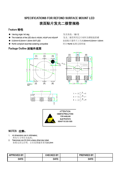
表面贴片发光二极管规格
升温速率及时间条件设定如下图所示
REFLOW PROFILE MAX.
10 SEC. MAX.
温度要求(电路板表面) RECOMMEND PAD DESIGN (Units: mm) 推荐焊盘设计(单位:毫米)
260 230 200 170 140 110 80 50 20
TEMPERATURE C
Package Outline 封装外观图
[1] [3] [5] [2] [4] [6]
[1]
polarity mark
[3]
[5]
[2]
[4]
[6]
1 3 5
G R B
2 4 6
ATTENTION
OBSERVE PRECAUTIONS FOR HANDLING ELECTROSTATIC SENSITIVE DEVICES
ILLUSION LED LIMITED
Typical optical characteristics curves 典型光电特性曲线
Spectral Distribution
) Relative Intensity vs. Wavelength (Ta=25 ° C ) Forward Voltage vs. Forward Current (Ta=25 ° C ) Relative Intensity vs. Forward Current (Ta=25 ° C
• After reflow soldering rapid cooling should be avoided 回流焊结束后避免快速冷却
Temperature-profile (Surface of circuit board)
Use the following conditions shown in the figure.
Karl Knauer首推OLEDs发光包装
20GREEN PACKAGING一些豁免原则,一些安全性没有问题或者可以通过其他物质予以验证的物质可以不需要进行许可列在法规名单中而直接允许使用,如美国法规阈值(TOR)原则,欧盟功能阻隔层内物质迁移量低于0.01mg/kg 的物质豁免原则、酸酚醇原则等。
美国和欧盟还以不同方式规定了禁止用于食品包装材料的物质。
为了排除食品包装材料的化学残留物对消费者的健康的威胁,欧美各国都颁布了一系列食品接触材料与制品安全性的相关法令。
但是,各国法规之间的差别是很大的,会给包装公司的生产贸易带来很大的问题。
近年来,我国频繁收到欧盟对我国出口食品接触性材料的卫生预警通报,由于我国出口的某些食品包装材料卫生指标不符合进口国要求而拒绝进口,给企业造成了巨大经济损失。
因此,宁波检验检疫部门提醒相关出口企业:一方面要求相关食品企业应加强食品包装材料卫生质量控制,熟悉进口国对包装材料本身的卫生标准要求;另一方面应加强食品包装材料卫生安全领域的科研与制标工作,以应对发达国家在该领域对我国设置的贸易技术壁垒,保障企业的经济利益与消费者的饮食安全。
塑料包装和塑料技术部件成德国塑料业增长推动力相关数据显示,2015年德国塑料行业营业额达到598亿欧元,其营业额比上一年增长1.3%。
德国是欧洲塑料业最大的生产地与加工地,德国塑料加工工业协会称,其营业额呈现出增长趋势,主要归功于塑料包装和塑料技术部件。
根据该协会统计,德国塑料加工业去年共雇用31.6万员工,其中规模在20人及以上的企业有2853家,塑料产品总产量达1360万吨。
“在过去几年中,德国的汽车工业成为许多工业领域发展的推动力,例如电子,化学和芯片工业。
由于环保的原因,减轻汽车的重量至关重要。
”德国联邦外贸与投资署专家Thorsten Bug 博士表示,由于上述原因,汽车工业也推动塑料工业,尤其超轻质塑料组件开发的发展。
Karl Knauer 首推OLEDs 发光包装通过与来自柏林的INURU GmbH 公司的合作, Karl Knauer 推出了全世界真正意义上的首个发光包装,这是一种以电子印刷过的柔性的有机发光二极管(OLEDs)为主要载体的包装,这也是该公司下一步发展的重点所在,该公司将对“HiLight- 印刷电子”技术做进一步的研究和发展。
- 1、下载文档前请自行甄别文档内容的完整性,平台不提供额外的编辑、内容补充、找答案等附加服务。
- 2、"仅部分预览"的文档,不可在线预览部分如存在完整性等问题,可反馈申请退款(可完整预览的文档不适用该条件!)。
- 3、如文档侵犯您的权益,请联系客服反馈,我们会尽快为您处理(人工客服工作时间:9:00-18:30)。
HB LED&LED PACKAGING’09 HB LED & LED PACKAGING ’09 Process, equipment and materialsTechnology and market trendsSAMPLEIR45 rue Sainte Geneviève, F-69006 Lyon, FranceOsramTel : +33 472 83 01 80 -Fax : +33 472 83 01 83Table of ContentContentIntroductionExecutive summary Acronyms & definitions LED market statusMarket segmentation •DICING–Location of Dicing Process–Saw Dicing–Laser Dicing–Saw VS Laser–Supply Chain–Market Volume for Sapphire Wafers•Market segmentation•Market Volume•Market Revenue•General Lighting•GaN-based White LEDs•Wafer Needs for General Lightingpp–Market Revenue for Dicing Services–Market of equipments in number of units–Market in $M•DIE BONDING–Location of the process–The Basics–Dispensing equipment from AsymtekLED Performance•Lumens. Depending on Applications•Internal Quantum Efficiency•Evolution Under High Current•Output Heat•Overall PerformancesDispensing equipment from Asymtek–Material for LED–Main players–Market Volume for Die Attach Material–Market Revenue for Die Attach Material–Market of equipments in number of units–Market of equipments in $M •INTERCONNECT•Expected Performances for White LED LED Packaging Status•Introduction•Package families•Assembly Process Flow INTERCONNECT–Location of the process–Overview of wire bonding–Electrical connection : the basics–Wire Bonding Processes–Ball bonding VS Wedge bonding–Ribbon bond VS wire bond–Main players–Definitions–Description–System Integration –Challenges–Value Chain–Evolution–TrendsMain players–Market revenue -Assumptions–Market revenue for gold wire bonding •ENCAPSULATION, LENS & PHOSPHOR–Location of the process–Encapsulation method for LED lamp–Casting process for encapsulationEncapsulation for SMD•Technology Roadmap •Packaging of Regular LED •Flow Chart for Regular LED –Main steps and materials–Standard Assembly Flow–Through Hole Devices–Surface Mount Devices –Encapsulation for SMD–Compression molding process–Materials for encapsulation–Market estimation of molding compound –How does LED generate white light?–Phosphor chemistry–Phosphor placement in white LEDMain phosphor technologies in use–Market Metrics -Packaged LED Market Volume –Main phosphor technologies in use –Main phosphor suppliers–Optics–Main playersTable of ContentPACKAGING OF HB/UBH ED Th l I f M i lPACKAGING OF HB/UBH LED•Introduction•What package for what LED? •Package type•Evolution of the packaging •Impact of the heatHB/UHB LED packaging function •INTERCONNECT–Location of the process–What’s new?–Evolution in wirebonding –Matrix LED –features –Flip Chip Technology –Wirebond VS Flip ChipFlip chip coupled with back face contact –Thermal Interface Material –Thermal Interface Material –Main Players –Heatsink–Heatsink –Main Players–Summary –LED Package with optimized heat transfer•HB/UHB LED packaging function •Different levels of packaging•Considerations of HB LED design •Materials challenges and solutions•Market Metrics -Packaged LED Market Volume •SCRIBING AND DICING–Location of the process –Flip-chip coupled with back-face contact reflector–Stud Bumping–Example of Lumileds Luxeon K2 –Laser Lift-Off (LLO) & Flip-Chip –Laser Lift Off Technique: definition –Laser Lift Off Technique: OSRAM –LLO equipment•ENCAPSULATION, LENS & PHOSPHOR–Location of the process–Optical extraction techniques –Remote phosphor–Silicon Product -Shin EtsuWAFER LEVEL PACKAGINGp–Scribing & Dicing: Definition–Techniques, Throughputs and Costs –Number of dice / wafer –Laser Scribing & Dicing –Diamond Scribing & Dicing–Example of JPSA Scribing & Dicing tool –Example of NWR Scribing & Dicing tool LLO equipment –LLO technique & Flip-chip mounting•TEMPORARY BONDING–introduction–Thin-wafer handling: different solutions –principleMain methods:a comparison •WAFER LEVEL PACKAGING –Main challenges for Power LED WLSP–Market drivers –Power LED Packaging –Power LED Packaging Manufacturer Motivations & Segmentation–3D-TSV developments for Power LEDs –Overview of power LED packaging types –Drivers for LED silicon packaging p g g–Laser Microjet Technology from Synova –Example of Synova Scribing & Dicing tool –Example of Oxford Lasers Scribing & Dicing tool–Example of ALSI Lasers Dicing tool –Stealth Dicing Technology –Stealth Dicing Roadmap–Main methods: a comparison –wax–adhesive tapes–EVG temporary bonding tools•THERMAL MANAGEMENT–Location of the process Thermal SolutionsDrivers for LED silicon packaging solutions–Supply chain focus on ESD protection using Si submounts for HB LEDs –Hymite: Silicon HB-LED packages –Silicon interposer for MEMS / LED Applications–3-D interposer to combine MOSFET + ASIC LED driver –Example of Stealth Laser Dicing tool –Example of Jenoptik-Votan dicing tool –Market Data -Assumptions –Laser vs saw–Market Revenue for HB/UHB LEDs–Market of equipment in number of units –Market revenue of equipments in $M–Thermal Solutions –Thermal solutions -Managing the LED Thermal System Configuration –Substrates–Substrates -SMD organic–Substrates -Metal Core Printed Circuit Board–Substrates -FR4 Board & Flexible ASIC LED driver–WLP : VisEra technologies–Estimation of 6” Silicon wafer demand for LED submount and WLP –Conclusion & challenges•CONCLUSION & CHALLENGES •DIE BONDING–Location of the process–Choosing die attach material–New material for HB/UHB LED -AuSn–AuSn –Strength and weakness of deposition methods –SummaryMarket Volume for Die Attach Material Substrate–Substrates -Ceramic Substrates –Substrates -Direct Bonded Copper –Substrates –Trends for DBC –Substrates -Summary–Substrates –Trends : Chip On Board –Substrates –Main Players •ANNEXES–Market Volume for Die Attach Material –Market Revenue for Die Attach Material–Market in number of die bonding equipment –Die bonding equipment –market in $M–Substrates –Market Data –Substrates –Market Volumes –Substrates –Market Revenue–HB LED submount –Market BreakdownLED Industry StatusSupply-ChainEPI WAFER WAFER PROCESSING EPI WAFERWAFER PROCESSINGPACKAGINGLED AssemblyFlow Chart for HB/UHB LEDScribing & Dicing¾saw ¾laserDie Bonding¾stencil printing ¾dispensing ¾jettingInterconnect¾Ball Bonding ¾Wedge Bonding ¾Flip Chip Th h Sili Vi ¾Through Silicon ViaThermal Management¾Substrate ¾Submount Phosphor & Encapsulation¾Remote Phosphor Dicing¾saw ¾laser¾Heat Slug¾molding ¾potting ¾castingLED Packaging StatusChallenges•Major requirements for LED package are :–Minimum light loss : improve LED efficiency–Thermal management : increase heat dissipation–Smaller size => cheaper–Specific assembly material, process and equipment => cheaper if fully automated Specific assembly material process and equipment=>cheaper if fully automated –Reducing the packaging cost to reduce the global LED manufacturing cost•Over the years, the input power has increased (HB & UHB LED) that Over the years the input power has increased(HB&UHB LED)thatproduces more lumens and so more heat is generated.•Several parameters have to be dramatically improved like : Several parameters have to be dramatically improved like:–Internal quantum efficiency (substrate level)–Electrical losses (die level)Extraction efficiency (die level)–Extraction efficiency(die level)–Phosphor conversion and optics quality (packaging level)LED industry have placed new requirements on packaging and assembly •LED industry have placed new requirements on packaging and assemblyChoices for package10000(mm 3)Overall volume of the package 10000the package 1000100100 100 0.1 1 10 100(W)PowerThermal ManagementLED Die •HB LED submount -Cree X-Lamp:LED Diep–Square shape LED silicon carrier submount withintegrated shottky diode for protection of ESDSilicon carrierSi carrierSubstrate with lens and phosphor removed, with the LEDdie assembly and bond wires in place (Courtesy ofMuAnalysis Inc.)Si carrier LED DiePlan view SEM image of the LED die mounted on Silicon submount (Courtesy of MuAnalysis Inc )on Silicon submount (Courtesy of MuAnalysis Inc.)Some of the recent Optical extraction techniques•Some of the recent techniques to improve light extraction efficiency–Silicon encapsulation and Silicon encapsulation and integrated secondary optics –Flip chip geometry –Thin film technology –Remote phosphor –Diffractive lenses –Photonic crystal ySubstrate –Current solutionsSilicon (TSV/WLP)0 %Substrates only70%Organic + Heat slug50%2008 Total HB/UHB LED MarketCeramic 20%S b t S b t t 30%Ceramic submount20%Submount + Substrates 30%Silicon submountSilicon submount 10%Wafer Level PackagingVisEra technologies•TSMC and its subsidiary VisEratechnologies has announced anew HB/UHB packagingtechnology based on 8” wafersgy•Features–Mass production (low cost)M d ti(l t)–Compatible with automatedequipment–Good thermal dissipation (5°C/W)Good thermal dissipation(5°C/W)–CTE compatible•Applications–Street lampsIndoor lighting–Indoor lightingCourtesy of VisEraPackaging of Regular LED Market size for materials。