4_Wire_PWM_Spec 1.3版
清华紫光 文诚系列电脑 说明书

文诚系列技术培训手册清华紫光台式电脑事业部技术支持部2004-06-01目录一、产品特点1.1优良的品质保证1.2出色的结构设计1.3可靠的安全维护二、文诚系列主机配置2.1文诚系列主机配置表三、主板技术规格3.1 精英P6VEMD2主板说明3.2 精英L4S5MG/GX+主板说明3.3 技嘉GA-8I845GV-CH2说明四、驱动程序安装4.1驱动光盘说明4.2驱动程序安装目录一、产品特点文诚系列电脑强调性能价格比,适用于教育、网吧等中低端用户,便于集中管理,统一维护。
1.1优良的品质保证1)通过国家3C认证;2)严格的部件优选体制,所有部件采用业界一线厂商的产品;3)周密的测试全集,保证部件的兼容性,同时保证系统的稳定性;4)五年保修。
1.2出色的结构设计1)立卧两用,根据不同空间随意放置;2)机箱面板模块化设计,根据不同的应用选取不同外观;3)良好的散热设计,确保立卧使用时系统内部热量有效、及时的散发;4)静音设计,减少部件共振,优化风道,降低噪音。
1.3可靠的安全维护1)集成硬盘保护功能,保证硬盘数据的安全,遭到破坏一键恢复;2)同一机型间网络传输功能,维护好一台机器即可通过网络对其他机器进行维护;3)自动维护,无人值班的情况下对整个网络环境中的机器机型维护;4)预留机箱锁孔,防止非法开启机箱。
二、文诚系列主机配置(一)文诚500 文诚800 文诚1000E 文诚1100文诚1200 CPU C3800Celeron 1.8GCeleron 1.8G Celeron 1.8G Celeron 1.8G主板 P6VEMD2L4S5MG/GX+ L4S5MG/GX+ L4S5MG/GX+GA-8I845GV-CH2内存Twinmos 128MDDR333Twinmos 128MDDR333Twinmos 128MDDR333Twinmos 128MDDR333Twinmos 128MDDR333硬盘SeagateST340015ASamsungSV0411N(40GB/5400PRM)SeagateST340015ASamsungSV0411N(40GB/5400PRM)SeagateST340015ASamsungSV0411N(40GB/5400PRM)光驱LG CR-8523B LG GCR-8523B软驱SamsungSFD-321BSamsungSFD-321BSamsungSFD-321B显示卡主板集成主板集成主板集成主板集成主板集成声卡主板集成主板集成主板集成主板集成主板集成网卡主板集成主板集成主板集成主板集成主板集成电源长城 1801-HP 长城 1801-HP 长城 1801-HP 长城 1801-HP 长城 1801-HPCPU风扇主板集成Cool MasterDI4-7H53B/DI4-7H54A-R2Cool MasterDI4-7H53B/DI4-7H54A-R2Cool MasterDI4-7H53B/DI4-7H54A-R2/EC203MBCool MasterDI4-7H53B/DI4-7H54A-R2/EC203MB机箱保利得 EN7472 保利得 EN7472 保利得 EN7472 保利得 EN7472 保利得 EN7472键盘精模 JME7010 精模 JME7010 精模 JME7010 精模 JME7010 精模 JME7010鼠标致伸 M042K0 致伸 M042K0 致伸 M042K0 致伸 M042K0 致伸 M042K0驱动光盘智能驱动光盘V2.0智能驱动光盘V2.0智能驱动光盘V2.0/2.1智能驱动光盘V2.0文诚系列主机配置(二)三、主板技术规格3.1文诚500采用的主板是:精英P6VEMD2,采用VIA CLE266 CE / VT8235 CD 芯片组。
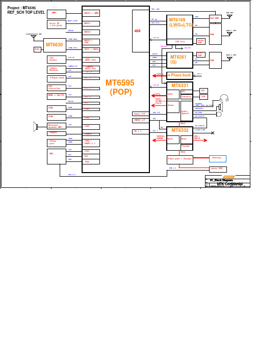
MT6595_MT6331_MT6332_ MT6169_MT6261_MT6630_EMMC_DSDA_EXTPWR_V0.03
Modules
I2C
C
I2C 4-Phase buck
CTP
I2C
controller
MEMs & ALS/PS I2C
GPIOs
SIM1
SIM1
SIM2
SIM2
B
External
I2S
speaker AMP.
Keypad
Debug port
JTAG UART
I2S
MHL
DPI
USB
A
USB 2.0
Front Camera
400 Kbps
Yes.
Front camera (OV5648) I2C address: 0X36 (Write:0x6C, Read:0x6D )
AF driver (AD5820) I2C address: 0X0C (Write:0x18, Read:0x19)
I2C-1
M Sensor
400 Kbps
AK8963C / M-Sensor I2C Address: 0x0C (Write:0x18, Read:0x19)
C
A+Gyro Sensor
400 Kbps
Yes.
MPU-6050C / A+Gyro I2C Address: 0x68 (Write:0xD0, Read:0xD1)
3
ABB
MT6595 (POP)
Audio I/F PWRAP I/F BC 1.1
3
2
1
BPI, APC
RXD ANT
RXD
RF IQ
Байду номын сангаасMT6169
RxD FEM
LS976- L79 spec cr1.3
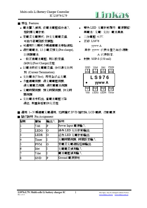
R7 10K
D1 1N5817 Q2 NPN, 3904
Layout:1A
Vdd LEDG LEDR GND Vdet Idet C3 0.1uf R4 330R LED2 Green 3 2 R8 C4 0.01uf 100K
U2 L431
BAT1 Li, 1S, 1000mAh
Remark: C3, C4 must close to U1 TimeOut Protect= 4.5hrs.
數 說 便
yyww A yyww : 年 / 數 A: . : SOP-8 (150 mil)
GND 8 Vdet 7 Idet 6 PWM 5
LS976
yyww A
1 Vdd 2 3 4 LEDG LEDR Timer
DVD, LCD源自, 行.1 2 3 4 5 6 7 8
Vdd LEDG LEDR Timer PWM Idet Vdet GND
Layout:2A
Rc 0R091, 1%, 1/4W Ic= 100mV / 0R091 ~ 1100mA
LS976-L79: Multi-cells Li battery charger IC
Rev. cr1.3
5
This Spec. may be changed without Notice.
Multi-cells Li Battery Charger Controller IC LS976-L79 Charge Curve
Vin Vpre Vbat Fast-Charge Ic Mode Pre-charge CC mode
Vfull
Charge termination
CV mode
綠 亮 亮 狀 ), 狀 ): 流= 10mA, LED( ) VDD.
三相电压型PWM整流器的仿真讲解
摘要为了解决电压型PWM整流器直接功率控制系统主电路参数设计问题,根据整流器在dq 两相同步旋转坐标系中的数学模型建立了其功率控制数学模型.基于功率控制数学模型,结合整流器直接功率控制系统的特点,推得交流侧电感是由功率、功率滞环比较器环宽及开关平均频率决定的;直流侧直流电压是由交流电压、电感及负载决定的;突加负载时直流侧电容是由直流电压波动、功率、电感及负载决定的.根据上述影响主电路参数的诸多因素,提出交流侧电感、直流侧电压及直流侧电容的设计方法.计算机仿真和实验证明了本文提出的设计方法是可行的.关键词PWM整流器; 直接功率控制; 直流电压; 交流侧电感; 直流电容目录1 电压型PWM整流器 (2)1.1电压型PWM整流器拓扑结构及数学模型 (3)1.2 电压型PWM整流器DPC系统结构及原理 (3)2 电压型PWM整流器DPC系统主电路参数设计 (5)2.1 交流侧电感的选择 (5)2.2 直流侧直流电压的选择 (6)2.3 直流侧电容的选择 (7)3 电压型PWM整流器DPC系统仿真与实验 (9)3.1 系统主电路参数设计 (9)3.2 系统仿真 (9)3.3 系统实验 (10)4 总结与体会 (12)参考文献 (13)1电压型PWM 整流器1.1电压型PWM 整流器拓扑结构及数学模型电压型PWM 整流器主电路拓扑结构如图1所示.图中a U ,b U ,c U 为三相对称电源相电压,,a b c i i i 为三相线电流;,,a b c S S S 为驱动整流器开关管(绝缘栅双极型晶体管IGBT)开关函数;jS 定义为单极性二值逻辑开关函数,jS =1(j=a,b,c)则上桥臂开关导通,下桥臂开关关断,jS =0下桥臂开关导通,上桥臂开关关断;dc U 为直流电压;R,L 为滤波电抗器的电阻和电感;C 为直流侧电容;RL 为负载;,ra rb rc U U U 为整流器的输入相电压;L i 为负载电流。
PCB工厂专业英语

標簽 層 電橋器 條形物 腳 漏 洩漏 漏電流 長度 線 線性的 組 電源線 列示 低的
米 儀表 儀器 磁鐵 磁石 磁性的 手冊 手工的 手動 邊緣 安全膠布 印章 最大值 測量 測量值 測試 外觀尺寸 迎合 滿足 符合 最小值 毫米 必須
材料明細表
BTO
Build To Order
接單生產
CAD/CAM Computer Aided Design/Manufactur CAR
Calibration Corrective Action Response
儀器校驗 (儀校) 改善對策報告
CCR
Customer Complain Requirement
客戶抱怨/要求
Charge Charge
索取費用
CND
Cannot Duplicate
無法複製,異常現象消失
CR
Critical
嚴重(CR>MA>MI)
CS
Customer Service
客戶服務
CTO
Configure To Order
接單組裝
Debit Note Debit Note
(會計) 帳目通知
測試工程
Total Productive Maintenance
全面性生產維護
Total Quality Management
全面品質管理
TUV
德國萊茵技術監護顧問公司 (安規單位)
Underwriters Laboratories
美國保險協會實驗室 (安規單位)
Vender Quality Approval
HV320WXC-200 Preliminary Product Spec Rev[1].P0_110412
![HV320WXC-200 Preliminary Product Spec Rev[1].P0_110412](https://img.taocdn.com/s3/m/4839e221192e45361066f527.png)
3.0 ELECTRICAL SPECIFICATIONS 3.1 TFT LCD Module
< Table 3. LCD Module Electrical Specifications > Parameter Power Supply Input Voltage Power Supply Ripple Voltage Power Supply Current Power Consumption Rush current Symbol VDD VRP IDD PDD IRUSH 266 3.2 Values Min 10.8 Typ 12 Max 13.2 300 525 6.3 3.0 Unit Vdc mV mA Watt A 1 2
A4(210 X 297)
PRODUCT GROUP
TFT- LCD PRODUCT SPEC. NUMBER SPEC. TITLE
REV P0
ISSUE DATE 2011.4.12 PAGE 7 OF 27
HV320WXC-200 Preliminary Product Specification Rev.P0
PRODUCT GROUP
TFT- LCD PRODUCT SPEC. NUMBER SPEC. TITLE
REV P0
ISSUE DATE 2011.4.12 PAGE 5 OF 27
HV320WXC-200 Preliminary Product Specification Rev.P0
1.3 Application
Pixel arrangement
Display colors Display mode Outline Dimension Weight Power Consumption Surface Treatment
联想电脑主板

07 POWER Map
08 GPIO
09 RESERVE
10 CPU LGA 1155_1
11 CPU LGA 1155_2
12 CPU LGA 1155_3
13 CPU LGA 1155_4
14 XDP/80 PORT HEADER
15 DDR3 CHA DIMM 0
16 Number: 10085
PAGE TITLE
Quantity
01 Cover Page
D
02 BLOCK DIAGRAM
03 Power Delivery
04 POWER GOOD AND RESET DIAGRAM
05 CLOCKS DIAGRAM
06 Power Sequence
Dual PWM Design
SLP_S3#
P-MOSFET AO4407
12V_S0
Bead
LDO UZ1085
5V_Codec
V_1P8_SFR Imax=1.6A
PANEL POWER CPU POWER
PWM TPS54331
VTT_PWRGD
PWM NCP6131
5V_LVDS Imax=2.2A
SPI BUS
FCBGA 989PIN ?X?mm
PCIE Gen1 Interface
LAN 82579ML
SATA *1
SATA2.0 BUS
B
Slim ODD
25M
RJ45
D
14.318MHz 33MHz 24MHz or 48MHz 96MHz 100 MHz 120 MHz
PCH CLOCK Buffer
Title
Switching Mode Power Supply Design

3.3V, 2.5V, 1.8V … for RAM, FPGA, I/O, DAC, etc.
AC/DC
Isolated DC/DC
Load DC/DCs
Load DC/DC
Linear Technology Confidential
-
+
T o f f
T o n
i n i V i n
O i V i n V
o
L i V o O i
+
+
S O F F
O N O F F O N
v D
V o V i+ n
i L I+ I i no V L i/ n F v S -/ F V L o
s s l e o p
Vo V in
i D I o
T o n
Input voltage range
Output voltage and current: Min / Max Output ripple Load transient Efficiency = PO / PIN = VOIO / VIN IIN
Linear Technology Confidential
• Choice of Solutions
• PCB Layout • Systematic Design Approach of Embedded Power
Linear Technology Confidential
2
Example of a Power Management System Embedded system
- 1、下载文档前请自行甄别文档内容的完整性,平台不提供额外的编辑、内容补充、找答案等附加服务。
- 2、"仅部分预览"的文档,不可在线预览部分如存在完整性等问题,可反馈申请退款(可完整预览的文档不适用该条件!)。
- 3、如文档侵犯您的权益,请联系客服反馈,我们会尽快为您处理(人工客服工作时间:9:00-18:30)。
4-Wire Pulse Width Modulation (PWM) Controlled FansSpecificationSeptember 2005Revision 1.3INFORMATION IN THIS DOCUMENT IS PROVIDED IN CONNECTION WITH INTEL® PRODUCTS. NO LICENSE, EXPRESS OR IMPLIED, BY ESTOPPEL OR OTHERWISE, TO ANY INTELLECTUAL PROPERTY RIGHTS IS GRANTED BY THIS DOCUMENT. EXCEPT AS PROVIDED IN INTEL’S TERMS AND CONDITIONS OF SALE FOR SUCH PRODUCTS, INTEL ASSUMES NO LIABILITY WHATSOEVER, AND INTEL DISCLAIMS ANY EXPRESS OR IMPLIED WARRANTY, RELATING TO SALE AND/OR USE OF INTEL PRODUCTS INCLUDING LIABILITY OR WARRANTIES RELATING TO FITNESS FOR A PARTICULAR PURPOSE, MERCHANTABILITY, OR INFRINGEMENT OF ANY PATENT, COPYRIGHT OR OTHER INTELLECTUAL PROPERTY RIGHT. Intel products are not intended for use in medical, life saving, or life sustaining applications.Intel may make changes to specifications and product descriptions at any time, without notice.The Intel® Pentium® 4 and Intel® Pentium® D processors may contain design defects or errors known as errata which may cause the product to deviate from published specifications. Current characterized errata are available on request.Contact your local Intel sales office or your distributor to obtain the latest specifications and before placing your product order.Intel and the Intel logo are trademarks or registered trademarks of Intel Corporation or its subsidiaries in the United States and other countries.*Other names and brands may be claimed as the property of others.Copyright © 2003-2005, Intel CorporationContents1Introduction (7)1.1Overview (7)2Electrical Specifications (9)2.1Fan Requirements (9)2.1.1Fan Input Voltage (9)2.1.2Current (9)2.1.3Tachometer Output Signal (9)2.1.4PWM Control Input Signal (9)2.2Test Methodology (10)2.3Hardware Monitor Device (10)2.3.1PWM Output Signal (10)2.4Considerations for Motherboard Designers (11)3Fan Speed Control (13)3.1Maximum Fan Speed Requirements (13)3.2Minimum Fan Speed Requirements (13)3.3Fan Speed Response to PWM Control Input Signal (14)3.4Operation below Minimum RPM (14)4Required Features (19)4.1.1Polarity Protection (19)4.1.2Rotor Lock Protection (19)4.1.3Wire Length (19)4.1.4Wire Type (19)4.1.5Connector Housing (19)4.1.6Fan Connector Pinout and Wiring Colors (19)5Environmental and Reliability (21)5.1.1Operating Temperature (21)5.1.2Non-operating Humidity (21)5.1.3Non-operating Thermal Cycling (21)5.1.4Power Cycling (21)5.1.5Reliability (21)6Reference Drawings (23)FiguresFigure 1. Screen Shot of PWM Duty Cycle (11)Figure 2 Minimum Fan Speed Requirements: Start Pulse (13)Figure 3 Fan Speed Response to PWM Control Input Signal (14)Figure 4 Type A Operation, Minimum RPM, Stay on at Minimum RPM (15)Figure 5 Type B Operation, Stay On at Minimum RPM, Off at 0% RPM (16)Figure 6 Type C, Operation below Minimum RPM, Min, RPM = Starting RPM (17)Figure 7 Connector Housing (24)Figure 8 Baseboard Connector (25)TablesTable 1 Connector Pinout (19)Revision HistoryRevision Number Description RevisionDate1.0 Initial Release Nov 2003 1.1 Corrected Tachometer input signal, added definitions to operating modes Dec 2003 1.2 Corrected Section2.4 PWM input parameter July 2004 1.3 Clarified & Expanded requirements on PWM for Hardware MonitorDevicesSept 2005§Introduction1 Introduction1.1 OverviewThis specification defines the intended operation of a fan that implements the Pulse WidthModulation (PWM) control signal on the 4-wire fan interface. The introduction of 4 wire PWMcontrolled fans is a means to reduce the overall system acoustics. The expectation is a 4 wirePWM controlled fan when properly implemented will be significantly quieter than a similar 3wire fan.§IntroductionElectricalSpecificationsSpecifications2 ElectricalRequirements2.1 Fan2.1.1 Fan Input VoltageFan operating voltage shall be within the range 12 V ±5% V.2.1.2 CurrentSteady state operation fan current draw (with 12.6 V applied, with fan operating in the free streamcondition) shall not exceed 1.5 A.Fan current spike during start-up operation (with 12.6 V applied, with fan operating in the freestream condition) shall be allowed to exceed 1.0 A, up to 2.2A maximum for a duration of nogreater than 1.0 sec.2.1.3 Tachometer Output SignalFan shall provide tachometer output signal with the following characteristics:•Two pulses per revolution•Open-collector or open-drain type output•Motherboard will have a pull up to 12V, maximum 12.6V2.1.4 PWM Control Input SignalThe following requirements are measured at the PWM (control) pin of the fan cable connector seeFigure 7 and Table 1:PWM Frequency: Target frequency 25 kHz, acceptable operational range 21 kHz to 28 kHzMaximum voltage for logic low: VIL = 0.8 VAbsolute maximum current sourced: Imax = 5 mA (short circuit current)Absolute maximum voltage level: VMax = 5.25 V (open circuit voltage)This signal must be pulled up to a maximum of 5.25V within the fan.Note:New fan designs are strongly encouraged to implement a 3.3V pull up for compatibility withbuffer design limits on Hardware Monitor Devices e.g. Super IO devices.Electrical SpecificationsMethodology2.2 TestTo measure the pull up and current sourced from the fan, power the fan to 13.2V and use a DMM(Digital Muli-meter).To verify the pull up value in the fan, measure the voltage between pin 4 (control) and pin 1(ground).To verify the current sourced by the fan, measure the current between pin 4 (control) and pin 1(ground).2.3 Hardware Monitor Device2.3.1 PWM Output SignalThe Hardware Monitor Devise is required to provide an open-drain or open-collector type outputfor the PWM signal on pin 4 (see Table 1 and Figure 8) with the following properties:Frequency: 25kHz nominal, 21-28kHz is acceptableCurrent sink capability: 5mA required, 8mA recommendedMaximum voltage capability: 5.25VMaximum VOL: 0.8VSignal is not inverted, 100% PWM results in Max fan speedElectricalSpecifications Figure 1. Screen Shot of PWM Duty CycleFigure 1 shows a PWM output operating at 25.3 kHz with a 77.9% duty cycle output with a fanhaving a ~ 5V pull up on the PWM signal.A 100% duty cycle would be a constant 5V signal with this fan and Hardware Monitor device.2.4 Considerations for Motherboard Designers1.The trace from PWM output to the fan header must not have a pull up or pull down. The pullup is located in the fan hub. The presence of a pull up on the motherboard will alter the fanresponse to the PWM Duty Cycle. In some cases this may prevent the fan from achievingfull speed even with the Hardware Monitor device issuing a 100% duty cycle.2.If driving multiple fans with a single PWM output, an open-drain / open collector outputbuffer circuit is required. Consult your Hardware Monitor vendor for layout suggestions.§Electrical SpecificationsFan Speed Control3 Fan Speed Control3.1 Maximum Fan Speed RequirementsThe maximum fan speed shall be specified for the fan model by the fan vendor and correspond to100% duty cycle PWM signal input.3.2 Minimum Fan Speed RequirementsThe vendor shall specify the minimum RPM and the corresponding PWM duty cycle. Thisspecified minimum RPM shall be 30% of maximum RPM or less. The fan shall be able to startand run at this RPM. To allow a lower specified minimum RPM, it is acceptable to provide ahigher PWM duty cycle to the fan motor for a short period of time for startup conditions. Thispulse should not exceed 30% maximum RPM and should last no longer than 2 seconds. SeeFigure 2.Figure 2 Minimum Fan Speed Requirements: Start PulseFan Speed Control3.3 Fan Speed Response to PWM Control Input SignalThe PWM input shall be delivered to the fan through the control signal on Pin 4 (see Section2.1.4). Fan speed response to this signal shall be a continuous and monotonic function of the dutycycle of the signal, from 100% to the minimum specified RPM. The fan RPM (as a percentage ofmaximum RPM) should match the PWM duty cycle within ±10%. If no control signal is presentthe fan shall operate at maximum RPM. See Figure 3.Figure 3 Fan Speed Response to PWM Control Input Signal3.4 Operation below Minimum RPMFor all duty cycles less than the minimum duty cycle, the RPM shall not be greater than theminimum RPM. The following graphs and definitions show three recommended solutions tohandle PWM duty cycles that are less than the minimum operational RPM, as a percentage ofmaximum.In a Type A implementation the fan will run at minimum RPM for all PWM duty cycle values lessthan minimum duty cycle. The minimum fan speed is controlled by design and can not beoverridden by the external fan speed controller. See Figure 4.Fan Speed Control Figure 4 Type A Operation, Minimum RPM, Stay on at Minimum RPMIn a Type B implementation the fan will run at minimum RPM for all non-zero PWM duty cyclevalues less than minimum duty cycle and turn off the motor at 0% PWM duty cycle. See Figure 5.Fan Speed ControlFigure 5 Type B Operation, Stay On at Minimum RPM, Off at 0% RPMIn Type C implementation the fan will stop running when the current provided to the motorwindings is insufficient to support commutation. The fan should not be damaged from this. Thefan would also turn off the motor at 0% PWM duty cycle input. See Figure 6.Fan Speed Control Figure 6 Type C, Operation below Minimum RPM, Min, RPM = Starting RPM§Fan Speed ControlFeaturesRequiredFeatures4 RequiredProtection4.1.1 PolarityFan motor shall have polarity protection.4.1.2 Rotor Lock ProtectionFan rotor shall have lock protection and auto-restart4.1.3 WireLengthTo be specified in individual fan specification based on applicationType4.1.4 WireWire type shall meet the following minimum qualifications: UL recognized appliance wiring,style UL1430, rated minimum 105C, 300V, 26 gauge.Housing4.1.5 ConnectorWire shall be terminated with 4-pin connector housing, Wieson part number 2510C888-001,Molex 47054-1000 or equivalent. See Figure 7 for reference drawingThe intended mating header for this connector housing, is Wieson part number 2366C888-007Molex 47053-1000, Foxconn HF27040-M1, Tyco 1470947-1 or equivalent See Figure 8 forreference drawing.4.1.6 Fan Connector Pinout and Wiring ColorsTable 1 Connector PinoutPin Function Wire Color1 GND BlackVYellow2 12Green3 Sense4 Control Blue§Required FeaturesEnvironmental and Reliability5 Environmental and ReliabilityTemperature5.1.1 OperatingFan shall be capable of sustaining normal operation over an ambient inlet temperature range of0°C to 70 °C.Humidity5.1.2 Non-operatingFan shall be capable of sustaining normal operation at +55 °C / 85 %R.H.5.1.3 Non-operating Thermal CyclingFan shall be capable of sustaining normal operation after being subjected to -5 °C to +70 °C for1000 cycles; ramp = 20 °C/min; 10 min dwell.Cycling5.1.4 PowerFan shall be capable of sustaining normal operation after being subjected to 7,500 on/off cycles,each cycle specified as 3 minutes on, 2 minutes off at 70°C ambient temperature. The sample sizeis 12 units for this test.5.1.5 ReliabilityMechanical wear out represents the highest risk reliability parameter for fans. The capability ofthe functional mechanical elements (ball / sleeve bearing, shaft, and tower assembly) must bedemonstrated to a minimum useful lifetime of 50,000 hours.The fan must pass the reliability test criteria with the fan operating at rated voltage in a hightemperature environment. Readouts include RPM, Icc and Noise. No infant mortality defectsallowed.Note:These are minimum requirements. The end customer should review vendor collateral and have their specific requirements reflected in a purchasing specification.§Environmental and ReliabilityReferenceDrawingsDrawings6 ReferenceThe following pages contain reference drawings for the Connector Housing, and BaseboardConnector.。