N3390-44.736中文资料
C3390中文资料
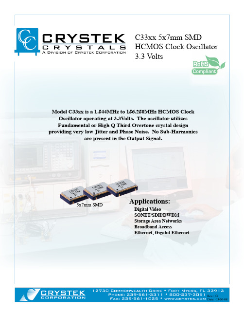
C33xx 5x7mm SMDHCMOS Clock Oscillator3.3 V oltsModel C33xx is a 1.544MHz to 156.250MHz HCMOS ClockOscillator operating at 3.3Volts. The oscillator utilizes Fundamental or High Q Third Overtone crystal design providing very low Jitter and Phase Noise. No Sub-Harmonicsare present in the Output Signal.Applications:5x7mm SMDDigital VideoSONET/SDH/DWDMStorage Area NetworksBroadband AccessEthernet, Gigabit EthernetHCMOS Clock Oscillator 3.3 V oltsC33xx 5x7mm SMD Frequency Range:1.544 to 156.250MhzFrequency Stability Options(ppm): ±20, ±25, ±50, ±100Temperature Range: (standard) 0°C to +70°C(Option M) -20°C to +70°C (Option E) -40°C to +85°C Storage: -55°C to 120°C Input Voltage: 3.3V ± 0.3V Input Current: (1.544~34.00MHz) 18mA Max (35.00~50.00MHz) 25mA Max (51.00~69.00MHz) 30mA Max (70.00~156.25MHz) 45mA MaxStandby Current: 3uA Typ., 10uA Max Output: HCMOSSymmetry: 45/55% Max @ 50%Vdd Rise/Fall Time: (1.54~10.00MHz) 5nsec Max @ 20% to 80% Vdd (10.10~30.00MHz) 4nsec Max @ 20% to 80% Vdd (30.10~50.00MHz) 3nsec Max @ 20% to 80% Vdd (50.10~80.00MHz) 2.5nsec Max @ 20% to 80% Vdd (80.10~156.25MHz) 2nsec Max @ 20% to 80% Vdd Logic: “0”= 10% Vdd Max“1”= 90% Vdd Min. Disable Time 200nSec MaxStart-up Time 1mSec Typ., 2mSec MaxLoad:30pF Max, >125MHz 15pF Max Jitter RMS:12KHz~80MHz0.5psec Typ., 1psec Max Sub-harmonics:NoneAging:<3ppm 1st/yr, <1ppm every year thereafterPART NUMBER GUIDEPart Number Stability C3390±100ppm C3392±50ppm C3391±25ppm C3398±20ppmExample: C3392-44.736MHzIntermediate Temp: CM3392-44.736MHz Extended Temp: CE3392-44.736MHzC = 0°C to 70°C CM = -20°C to 70°C CE = -40°C to 85°CHCMOS Clock Oscillator 3.3 V oltsC33xx 5x7mm SMDRECOMMENDED REFLOW SOLDERING PROFILE217°C 200°C 260°C 150°C90 Secs. Max.T E M P E R A T U R ERamp-Up 3°C/Sec Max.Preheat 180 Secs. Max.8 Minutes Max.260°C for 10 Secs. Max.CriticalTemperature ZoneRamp-Down 6°C/Sec.NOTE: Reflow Profile with 240°C peak also acceptable.0.045 ±0.008(1.14 ±0.20)0.055 Typ.(1.40 Typ.)0.200 ±0.005(5.08 ±0.13)#1#3#2#40.283(7.20)0.204(5.02)P/N XXX FrequencyXXDenotes pad 1XXX=Date Code XX=Lot Code 0.075 (1.80)PadConnection1Enable/Disable2GND 3Out 4VccSUGGESTED PAD LAYOUT0.071 SQ (1.80)0.165(4.19)0.200(5.08)0.01uF Bypass Capacitor RecommendedMechanical:Shock:Solderability:Vibration:Solvent Resistance:Resistance to Soldering Heat:Environmental:Thermal Shock:Moisture Resistance:MIL-STD-883, Method 2002, Condition B MIL-STD-883, Method 2003MIL-STD-883, Method 2007, Condition A MIL-STD-202, Method 215MIL-STD-202, Method 210, Condition I or JMIL-STD-883, Method 1011, Condition A MIL-STD-883, Method 1004Tri-State FunctionPin #1StateOutput State Open or N/C Active“1” level 0.7*Vcc Min Active “0” level 0.3*Vcc MaxHigh ZPWR SupplymA MVMOSC.pin 1pin 4pin 2pin 3Bypass Cap.O/P Load incl Probe ClOUTHigh Impedance GND or "LOW"Oscillation OPEN or "HIGH"GNDOUTVdd。
SEN-R-956-003中文资料

TECHNICAL DATA SHEET 4200…SURFACE MOUNT DIE WITH HEAT ABSORBING STANDOFF TERMINAL STRIPS TRANSIENT VOLTAGE SUPPRESSOR 500 WATT SERIES Glass Passivated Die Plus Dual Heat StripsFeatures:• Low Profile• Broad Voltage Range Available - - 6.8 to 200 Volts • Broad Spectrum Transient Suppression• Rapid Response - - 4 nanoseconds typical• Built-in Heat Absorbing Terminations• Electrically Similar to Mil-Prf-19500/516 Applications:• Connector I/O Surge Suppression• Data Line Protection Description: This is a bipolar transient voltage suppressor series extending from 6.8 volts to 200 volts intended for surface mount applications.Each device comes as a “Cell” with its own heat absorbing terminals pre-bonded at high temperature. This permits mounting on printed circuit boards that cannot provide their own heat sinking. Each terminal is silver plated and is solderable permitting solder down attachment with a very small footprint. Each unit is bi-symmetrical so any orientation can be used.ELECTRICAL CHARACTERISTICSPARAMETER SYMBOL Test Conditions Min TYP Max.Units Response Turn-on Time ton 2 5 nsTransient Energy Pulse (Cell) Ep 1 10uS rise, I= 0.5Ip at t=100us (exponentialdecay)1500 WTransient Energy Pulse (Cell) Ep 2 10uS rise, I= 0.5Ip at t=1.0mS (exponentialdecay)500 WTransient Energy Pulse (Cell) Ep 3 10uS rise, I= 0.5Ip at t=10mS (exponentialdecay)150 WTransient Energy Pulse (Cell) Ep 4 10uS rise, I= 0.5Ip at t=50mS (exponentialdecay)70 WTransient Energy Pulse(Cell)Ep 5 10uS rise, I= 0.5Ip at t=50mS (step pulse) 50 W Electrical Parameters See TableMaximum SolderTemperatureTmax 10 second exposure 300 ºC Thermal Resistance (J-C) ΤJC Assume heat sink on terminal strip ends 18 30 ºC/WNote 1: “Die Only” configuration requires user to provide adequate energy absorption. Note 2: Terminal strips are 0.009” to 0.011” thick copper with nickel and silver plate.0.034"0.039"Typ0.052"0.056"0.0115"0.0155"Bipolar Die OnlySEN-R-956-XXX 500Watt TVS SeriesNominal Vz min Vz max TC (nom) Ir max Part Vz Iz @ Iz @ Iz of Vz Vr @ Vr Vcc Ip Number (V) (mA) (V) (V) (%.°C) (V) (uA) (V) (A) SEN-R-956-001 6.8 10 6.40 7.25 0.050 5.0 1600 9.2 54.3 SEN-R-956-002 7.2 10 6.67 7.67 0.060 6.0 1600 10.3 48.5 SEN-R-956-003 7.8 10 7.22 8.30 0.060 6.5 1000 11.2 44.6 SEN-R-956-004 8.4 10 7.78 8.95 0.060 7.0 400 12.0 41.7 SEN-R-956-005 9.0 1 8.33 9.58 0.070 7.5 200 12.9 38.8 SEN-R-956-006 9.6 1 8.89 10.23 0.070 8.0 100 13.6 36.8 SEN-R-956-007 10 1 9.44 10.82 0.070 8.5 20 14.4 34.7 SEN-R-956-008 11 1 10.00 11.50 0.080 9.0 10 15.4 32.5 SEN-R-956-009 12 1 11.10 12.80 0.080 10.0 5 17.0 29.4 SEN-R-956-010 13 1 12.20 14.00 0.080 11.0 5 18.2 27.5 SEN-R-956-011 14 1 13.30 15.50 0.085 12.0 5 19.9 25.1 SEN-R-956-012 15 1 14.40 16.50 0.085 13.0 5 21.5 23.3 SEN-R-956-013 17 1 15.60 17.90 0.085 14.0 5 23.2 21.6 SEN-R-956-014 18 1 16.70 19.20 0.090 15.0 5 24.4 20.5 SEN-R-956-015 19 1 17.80 20.50 0.090 16.0 5 26.0 19.2 SEN-R-956-016 20 1 18.90 21.70 0.090 17.0 5 27.6 18.1 SEN-R-956-017 22 1 20.00 23.30 0.095 18.0 5 29.2 17.1 SEN-R-956-018 24 1 22.20 25.50 0.095 20.0 5 32.4 15.4 SEN-R-956-019 26 1 24.40 28.00 0.095 22.0 5 35.5 14.1 SEN-R-956-020 29 1 26.70 30.70 0.095 24.0 5 38.9 12.9 SEN-R-956-021 31 1 28.90 33.20 0.095 26.0 5 42.1 11.9 SEN-R-956-022 33 1 31.10 35.80 0.095 28.0 5 45.4 11.0 SEN-R-956-023 36 1 33.30 38.30 0.095 30.0 5 48.4 10.3 SEN-R-956-024 39 1 36.70 42.20 0.100 33.0 5 53.3 9.4 SEN-R-956-025 43 1 40.00 46.00 0.100 36.0 5 58.1 8.6 SEN-R-956-026 48 1 44.40 51.10 0.100 40.0 5 64.5 7.8 SEN-R-956-027 51 1 47.80 54.90 0.100 43.0 5 69.4 7.2 SEN-R-956-028 54 1 50.00 57.50 0.100 45.0 5 72.7 6.9 SEN-R-956-029 57 1 53.30 61.30 0.100 48.0 5 77.4 6.5 SEN-R-956-030 61 1 56.7 65.2 0.100 51.0 5 82.4 6.1 SEN-R-956-031 65 1 60.0 69.0 0.100 54.0 5 87.1 5.7 SEN-R-956-032 69 1 64.4 74.1 0.105 58.0 5 93.6 5.3 SEN-R-956-033 72 1 66.7 76.7 0.105 60.0 5 96.8 5.2 SEN-R-956-034 76 1 71.1 81.8 0.105 64.0 5 103.0 4.9 SEN-R-956-035 84 1 77.8 89.5 0.110 70.0 5 113.0 4.4 SEN-R-956-036 90 1 83.3 95.8 0.110 75.0 5 121.0 4.1 SEN-R-956-037 93 1 86.7 99.7 0.110 78.0 5 126.0 4.0 SEN-R-956-038 101 1 94.4 108.2 0.110 85.0 5 137.0 3.6 SEN-R-956-039 108 1 100.0 115.5 0.110 90.0 5 146.0 3.4 SEN-R-956-040 120 1 111.0 128.0 0.110 100.0 5 162.0 3.1 SEN-R-956-041 131 1 122.0 140.5 0.110 110.0 5 177.0 2.8 SEN-R-956-042 143 1 133.0 153.0 0.110 120.0 5 193.0 2.6 SEN-R-956-043 155 1 144.0 165.5 0.110 130.0 5 209.0 2.4 SEN-R-956-044 180 1 167.0 192.5 0.110 150.0 5 243.0 2.1 SEN-R-956-045 192 1 178.0 205.0 0.110 160.0 5 259.0 1.9 SEN-R-956-046 203 1 189.0 217.5 0.110 170.0 5 275.0 1.81Time (s)Clamp Power vs Time for Sensitron 500W TVS SeriesTime (mS)Exponential Decay Pulse WaveformRated Vz of Device (V)Reverse Junction Capacitance for Sensitron 500W TVSSENSITRONSEMICONDUCTORTECHNICAL DATADISCLAIMER:1- The information given herein, including the specifications and dimensions, is subject to change without prior notice to improve product characteristics. Before ordering, purchasers are advised to contact the Sensitron Semiconductor sales department for the latest version of the datasheet(s).2- In cases where extremely high reliability is required (such as use in nuclear power control, aerospace and aviation, traffic equipment, medical equipment, and safety equipment), safety should be ensured by using semiconductor devices that feature assured safety or by means of users’ fail-safe precautions or other arrangement.3- In no event shall Sensitron Semiconductor be liable for any damages that may result from an accident or any other cause during operation of the user’s units according to the datasheet(s). Sensitron Semiconductor assumes no responsibility for any intellectual property claims or any other problems that may result from applications of information, products or circuits described in the datasheets.4- In no event shall Sensitron Semiconductor be liable for any failure in a semiconductor device or any secondary damage resulting from use at a value exceeding the absolute maximum rating.5- No license is granted by the datasheet(s) under any patents or other rights of any third party or Sensitron Semiconductor.6- The datasheet(s) may not be reproduced or duplicated, in any form, in whole or part, without the expressed written permission of Sensitron Semiconductor.7- The products (technologies) described in the datasheet(s) are not to be provided to any party whose purpose in their application will hinder maintenance of international peace and safety nor are they to be applied to that purpose by their direct purchasers or any third party. When exporting these products (technologies), the necessary procedures are to be taken in accordance with related laws and regulations.。
2N3906中文资料(nte)中文数据手册「EasyDatasheet - 矽搜」
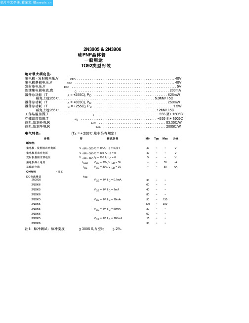
VCE = 1V, I C = 1mA
40 − − 80 − −
2N3905 2N3906
VCE = 1V, I C = 10mA
50 − 150 100 − 300
2N3905 2N3906
VCE = 1V, I C = 50mA
30 − − 60 − −
2N3905 2N3906
VCE = 1V, I C = 100mA
芯片中文手册,看全文,戳
2N3905 & 2N3906 硅PNP晶体管
一般用途
TO92类型封装
绝对最大额定值:
集电极 - 发射极电压,V
CEO . . . . . . . . . . . . . . . . . . . . . . . . . . . . . . . . . . . . . . . . . . . . . . . . . . . . . . 40V
器件总功耗(T
C = +255C), PD . . . . . . . . . . . . . . . . . . . . . . . . . . . . . . . . . . . . . . . . . . . . 1.5W
减免上述255℃. . . . . . . . . . . . . . . . . . . . . . . . . . . . . . . . . . . . . . . . . . . . . . . . . . . . . . 12MW / 5C
减免上述255℃. . . . . . . . . . . . . . . . . . . . . . . . . . . . . . . . . . . . . . . 5.0MW / 5C
器件总功耗(T
4N33-X000中文资料

Optocoupler, Photodarlington Output, High Gain, with Base Connection 4N32/4N33Vishay SemiconductorsDESCRIPTIONThe 4N32 and 4N33 are optically coupled isolators with a gallium arsenide infrared LED and a solicon photodarlington sensor.Switching can be achieved while maintaining a high degree of isolation between driving and load circuits.These optocouplers can be used to replace reed and mercury relays with advantages of long life, high speed switching and elimination of magnetic fields.FEATURES•Very high current transfer ratio, 500 % min.•High isolation resistance, 1011Ω typical •Standard plastic DIP package•Lead (Pb)-free component•Component in accordance to RoHS 2002/95/EC and WEEE 2002/96/ECAGENCY APPROVALS•UL1577, file no. E76222 system code A•DIN EN 60747-5-5 available with option 1•BSI IEC 60950; IEC 60065ORDER INFORMATIONPART REMARKS4N32CTR > 500 %, DIP-64N33CTR > 500 %, DIP-6ABSOLUTE MAXIMUM RATINGS (1)PARAMETER TEST CONDITION SYMBOL VALUE UNIT INPUTReverse voltage V R 6.0V Forward current I F60mAPower dissipation P diss100mWDerate linearly from 55 °C 1.33mW/°C OUTPUTCollector emitter breakdown voltage BV CEO30VEmitter base breakdown voltage BV EBO8.0V Collector base breakdown voltage BV CBO50VEmitter collector breakdown voltage BV ECO 5.0V Collector (load) current I C150mAPower dissipation P diss150mWDerate linearly 2.0mW/°CDocument Number: 83736For technical questions, contact: optocoupler.answers@ For technical questions, contact: optocoupler.answers@Document Number: 837364N32/4N33Vishay Semiconductors Optocoupler, Photodarlington Output,High Gain, with Base ConnectionNotes (1)T amb = 25 °C, unless otherwise specified.Stresses in excess of the absolute maximum ratings can cause permanent damage to the device. Functional operation of the device is not implied at these or any other conditions in excess of those given in the operational sections of this document. Exposure to absolute maximum ratings for extended periods of the time can adversely affect reliability.(2)Refer to wave profile for soldering conditions for through hole devices.Notes(1)T amb = 25 °C, unless otherwise specified.Minimum and maximum values are testing requirements. Typical values are characteristics of the device and are the result of engineering evaluation. Typical values are for information only and are not part of the testing requirements.(2)Indicates JEDEC registered values.COUPLER Total dissipation P tot250mW Derate linearly 3.3mW/°C Isolation test voltage V ISO 5300V RMS Leakage path 7.0mm min.Air path7.0mm min.Isolation resistance V IO = 500 V, T amb = 25 °C R IO ≥ 1012ΩV IO = 500 V, T amb = 100 °CR IO ≥ 1011ΩStorage temperature T stg - 55 to + 125°C Operating temperature T amb - 55 to + 100°C Lead soldering time (2)at 260 °C10sELECTRICAL CHARACTERISTICS (1)PARAMETER TEST CONDITIONSYMBOLMIN.TYP.MAX.UNIT INPUTForward voltage I F = 50 mA V F 1.25 1.5V Reverse current V R = 3.0 V I R 0.1100µA Capacitance V R = 0 V C O 25pF OUTPUTCollector emitter breakdown voltage (2)I C = 100 µA, I F = 0BV CEO 30V Collector base breakdown voltage (2)I C = 100 µA, I F = 0BV CBO 50V Emitter base breakdown voltage (2)I C = 100 µA, I F = 0BV EBO 8VEmitter collector breakdown voltage (2)I C = 100 µA, I F = 0BV ECO 510V Collector emitter leakage current V CE = 10 V, I F = 0I CEO 1.0100nA COUPLERCollector emitter saturation voltage V CEsat1.0V Coupling capacitance1.5pFCURRENT TRANSFER RATIOPARAMETER TEST CONDITION SYMBOL MIN.TYP.MAX.UNIT Current transfer ratioV CE = 10 V, I F = 10 mACTR500%SWITCHING CHARACTERISTICSPARAMETER TEST CONDITION SYMBOLMIN.TYP.MAX.UNIT Turn-on time V CC = 10 V, I C = 50 mA t on 5.0µs Turn-off timeI F = 200 mA, R L = 180 Ωt off100µsABSOLUTE MAXIMUM RATINGS (1)PARAMETER TEST CONDITIONSYMBOLVALUEUNIT4N32/4N33Optocoupler, Photodarlington Output,High Gain, with Base ConnectionVishay SemiconductorsNoteAs per IEC 60747-5-2, § 7.4.3.8.1, this optocoupler is suitable for "safe electrical insulation" only within the safety ratings. Compliance with the safety ratings shall be ensured by means of protective circuits.TYPICAL CHARACTERISTICST amb = 25 °C, unless otherwise specifiedFig. 1 - Normalized Non-Saturated and Saturated CTR CE vs.LED Current Fig. 2 - Normalized Non-Saturated and Saturated Collector EmitterCurrent vs. LED CurrentSAFETY AND INSULATION RATINGSPARAMETER TEST CONDITION SYMBOL MIN.TYP.MAX.UNIT Climatic classification(according to IEC 68 part 1)55/100/21Comparative tracking index CTI175399Peak transient overvoltage V IOTM6000V Peak insulation voltage V IORM850V Safety rating - power output P SO265mW Safety rating - input current I SI130mA Safety rating - temperature T SI150°C Creepage distance standard DIP-67mm Clearance distance standard DIP-67mm Creepage distance400 mil DIP-68mm Clearance distance400 mil DIP-68mmInsulation thickness,reinforced ratedper IEC 60950 2.10.5.10.4mmDocument Number: 83736For technical questions, contact: optocoupler.answers@ 4N32/4N33Vishay Semiconductors Optocoupler, Photodarlington Output,High Gain, with Base ConnectionFig. 3 - Normalized Collector Base Photocurrent vs.LED CurrentFig. 4 - Non-Saturated and Saturated h FE vs.Base CurrentFig. 5 - Low to High Propagation Delay vs.Collector Load Resistance and LED CurrentFig. 6 - High to Low Propagation Delay vs.Collector Load Resistance and LED Current Fig. 7 - Switching Waveform and Switching Schematic For technical questions, contact: optocoupler.answers@ Document Number: 837364N32/4N33Optocoupler, Photodarlington Output,Vishay SemiconductorsHigh Gain, with Base ConnectionPACKAGE DIMENSIONS in millimetersFor 4N32/33.... see DIL300-6 Package dimension in the package section.For products with an option designator (e.g. 4N32-X007 or 4N33-X009).... see DIP-6 Package dimensions in the package section. DIL300-6 Package DimensionsDIP-6 Package DimensionsDocument Number: 83736For technical questions, contact: optocoupler.answers@ 4N32/4N33Vishay Semiconductors Optocoupler, Photodarlington Output,High Gain, with Base Connection For technical questions, contact: optocoupler.answers@ Document Number: 837364N32/4N33Optocoupler, Photodarlington Output,Vishay SemiconductorsHigh Gain, with Base ConnectionOZONE DEPLETING SUBSTANCES POLICY STATEMENTIt is the policy of Vishay Semiconductor GmbH to1.Meet all present and future national and international statutory requirements.2.Regularly and continuously improve the performance of our products, processes, distribution and operating systems withrespect to their impact on the health and safety of our employees and the public, as well as their impact on the environment. It is particular concern to control or eliminate releases of those substances into the atmosphere which are known as ozone depleting substances (ODSs).The Montreal Protocol (1987) and its London Amendments (1990) intend to severely restrict the use of ODSs and forbid their use within the next ten years. Various national and international initiatives are pressing for an earlier ban on these substances. Vishay Semiconductor GmbH has been able to use its policy of continuous improvements to eliminate the use of ODSs listed in the following documents.1.Annex A, B and list of transitional substances of the Montreal Protocol and the London Amendments respectively.2.Class I and II ozone depleting substances in the Clean Air Act Amendments of 1990 by the Environmental Protection Agency(EPA) in the USA.3.Council Decision 88/540/EEC and 91/690/EEC Annex A, B and C (transitional substances) respectively.Vishay Semiconductor GmbH can certify that our semiconductors are not manufactured with ozone depleting substances and do not contain such substances.We reserve the right to make changes to improve technical designand may do so without further notice.Parameters can vary in different applications. All operating parameters must be validated for each customer application by the customer. Should the buyer use Vishay Semiconductors products for any unintended or unauthorized application, the buyer shall indemnify Vishay Semiconductors against all claims, costs, damages, and expenses, arising out of, directly or indirectly, any claim of personal damage, injury or death associated with such unintended or unauthorized use.Vishay Semiconductor GmbH, P.O.B. 3535, D-74025 Heilbronn, GermanyDocument Number: 83736For technical questions, contact: optocoupler.answers@ Disclaimer Legal Disclaimer NoticeVishayAll product specifications and data are subject to change without notice.Vishay Intertechnology, Inc., its affiliates, agents, and employees, and all persons acting on its or their behalf (collectively, “Vishay”), disclaim any and all liability for any errors, inaccuracies or incompleteness contained herein or in any other disclosure relating to any product.Vishay disclaims any and all liability arising out of the use or application of any product described herein or of any information provided herein to the maximum extent permitted by law. The product specifications do not expand or otherwise modify Vishay’s terms and conditions of purchase, including but not limited to the warranty expressed therein, which apply to these products.No license, express or implied, by estoppel or otherwise, to any intellectual property rights is granted by this document or by any conduct of Vishay.The products shown herein are not designed for use in medical, life-saving, or life-sustaining applications unless otherwise expressly indicated. Customers using or selling Vishay products not expressly indicated for use in such applications do so entirely at their own risk and agree to fully indemnify Vishay for any damages arising or resulting from such use or sale. Please contact authorized Vishay personnel to obtain written terms and conditions regarding products designed for such applications.Product names and markings noted herein may be trademarks of their respective owners.元器件交易网Document Number: 。
标准电阻阻值表67824

国家标准规定了电阻的阻值按其精度分为两大系列,分别为E-24系列和E-96系列,E-24系列精度为5%,E-96系列为1%。
精度为5%的碳膜电阻,以欧姆为单位的标称值:1.0 5.6 33 160 820 3.9K 20K 100K 510K2.7M1.1 6.2 36 180 910 4.3K 22K 110K 560K 3M1.2 6.8 39 200 1K 4.7K 24K 120K 620K 3.3M1.3 7.5 43 220 1.1K 5.1K 27K 130K 680K 3.6M1.5 8.2 47 240 1.2K 5.6K 30K 150K 750K 3.9M1.6 9.1 51 270 1.3K 6.2K 33K 160K 820K 4.3M1.8 10 56 300 1.5K 6.6K 36K 180K 910K 4.7M2.0 11 62 330 1.6K 7.5K 39K 200K 1M 5.1M2.2 12 68 360 1.8K 8.2K 43K 220K 1.1M 5.6M2.4 13 75 390 2K 9.1K 47K 240K 1.2M 6.2M2.7 15 82 430 2.2K 10K 51K 270K 1.3M 6.8M3.0 16 91 470 2.4K 11K 56K 300K 1.5M 7.5M3.3 18 100 510 2.7K 12K 62K 330K 1.6M 8.2M3.6 20 110 560 3K 13K 68K 360K 1.8M 9.1M3.9 22 120 620 3.2K 15K 75K 390K 2M 10M4.3 24 130 680 3.3K 16K 82K 430K 2.2M 15M4.7 27 150 750 3.6K 18K 91K 470K 2.4M 22M5.1 30精度为1%的金属膜电阻,以欧姆为单位的标称值:10 33 100 332 1K 3.32K 10.5K 34K 107K 357K10.2 33.2 102 340 1.02K 3.4K 10.7K 34.8K 110K 360K10.5 34 105 348 1.05K 3.48K 11K 35.7K 113K 365K10.7 34.8 107 350 1.07K 3.57K 11.3K 36K 115K 374K11 35.7 110 357 1.1K 3.6K 11.5K 36.5K 118K 383K11.3 36 113 360 1.13K 3.65K 11.8K 37.4K 120K 390K11.5 36.5 115 365 1.15K 3.74K 12K 38.3K 121K 392K11.8 37.4 118 374 1.18K 3.83K 12.1K 39K 124K 402K12 38.3 120 383 1.2K 3.9K 12.4K 39.2K 127K 412K12.1 39 121 390 1.21K 3.92K 12.7K 40.2K 130K 422K12.4 39.2 124 392 1.24K 4.02K 13K 41.2K 133K 430K12.7 40.2 127 402 1.27K 4.12K 13.3K 42.2K 137K 432K13 41.2 130 412 1.3K 4.22K 13.7K 43K 140K 442K13.3 42.2 133 422 1.33K 4.32K 14K 43.2K 143K 453K13.7 43 137 430 1.37K 4.42K 14.3K 44.2K 147K 464K14 43.2 140 432 1.4K 4.53K 14.7K 45.3K 150K 470K14.3 44.2 143 442 1.43K 4.64K 15K 46.4K 154K 475K14.7 45.3 147 453 1.47K 4.7K 15.4K 47K 158K 487K15 46.4 150 464 1.5K 4.75K 15.8K 47.5K 160K 499K15.4 47 154 470 1.54K 4.87K 16K 48.7K 162K 511K15.8 47.5 158 475 1.58K 4.99K 16.2K 49.9K 165K 523K16 48.7 160 487 1.6K 5.1K 16.5K 51K 169K 536K16.2 49.9 162 499 1.62K 5.11K 16.9K 51.1K 174K 549K16.5 51 165 510 1.65K 5.23K 17.4K 52.3K 178K 560K16.9 51.1 169 511 1.69K 5.36K 17.8K 53.6K 180K 562K17.4 52.3 174 523 1.74K 5.49K 18K 54.9K 182K 576K17.8 53.6 178 536 1.78K 5.6K 18.2K 56K 187K 590K18 54.9 180 549 1.8K 5.62K 18.7K 56.2K 191K 604K18.2 56 182 560 1.82K 5.76K 19.1K 57.6K 196K 619K18.7 56.2 187 562 1.87K 5.9K 19.6K 59K 200K 620K19.1 57.6 191 565 1.91K 6.04K 20K 60.4K 205K 634K19.6 59 196 578 1.96K 6.19K 20.5K 61.9K 210K 649K20 60.4 200 590 2K 6.2K 21K 62K 215K 665K20.5 61.9 205 604 2.05K 6.34K 21.5K 63.4K 220K 680K21 62 210 619 2.1K 6.49K 22K 64.9K 221K 681K21.5 63.4 215 620 2.15K 6.65K 22.1K 66.5K 226K 698K22 64.9 220 634 2.2K 6.8K 22.6K 68K 232K 715K22.1 66.5 221 649 2.21K 6.81K 23.2K 68.1K 237K 732K22.6 68 226 665 2.26K 6.98K 23.7K 69.8K 240K 750K23.2 68.1 232 680 2.32K 7.15K 24K 71.5K 243K 768K23.7 69.8 237 681 2.37 7.32K 24.3K 73.2K 249K 787K24 71.5 240 698 2.4K 7.5K 24.9K 75K 255K 806K24.3 73.2 243 715 2.43K 7.68K 25.5K 76.8K 261K 820K24.7 75 249 732 2.49K 7.87K 26.1K 78.7K 267K 825K24.9 75.5 255 750 2.55K 8.06K 26.7K 80.6K 270K 845K25.5 76.8 261 768 2.61K 8.2K 27K 82K 274K 866K26.1 78.7 267 787 2.67K 8.25K 27.4K 82.5K 280K 887K26.7 80.6 270 806 2.7K 8.45K 28K 84.5K 287K 909K27 82 274 820 2.74K 8.66K 28.7K 86.6K 294K 910K27.4 82.5 280 825 2.8K 8.8K 29.4K 88.7K 300K 931K28 84.5 287 845 2.87K 8.87K 30K 90.9K 301K 953K28.7 86.6 294 866 2.94K 9.09K 30.1K 91K 309K 976K29.4 88.7 300 887 3.0K 9.1K 30.9K 93.1K 316K 1.0M30 90.9 301 909 3.01K 9.31K 31.6K 95.3K 324K 1.5M30.1 91 309 910 3.09K 9.53K 32.4K 97.6K 330K 2.2M30.9 93.1 316 931 3.16K 9.76K 33K 100K 332K31.6 95.3 324 953 3.24K 10K 33.2K 102K 340K32.4 97.6 330 976 3.3K 10.2K 33.6K 105K 348K常用电阻阻值:1,1.1,1.2,1.3,1.5,1.6,1.8 2,2.2,2.4,2.7,3,3.3,3.6,3.9 4.3,4.7 5.1,5.6 6.2,6.8 7.5 8.29.1 10,11,12,13,15,16,1820,22,24,2730,33,36,3943,4751,5662,687582,81 100,110,120,130,150 ,160,180200,220,240,270300,330,360,390430,470510,560620,680750820910 1K,1.1K,1.2K,1.3K,1.5K,1.6K,1.8K 2K,2.2K,2.4K,2.7K 3K,3.3K,3.6K,3.9K 4.3K,4.7K 5.1K,5.6K 6.2K,6.8K,7.5K 8.2K 9.1K10K,11K ,12K,13K,15K,16K,18K20K,22K,24K,27K30K,33K,36K,39K43K,47K 51K,56K62K,68K75K82K91K 100K,110K,120K,130K,150K,160K,180K 200K,220K,240K,270K,300K,330K,360K,390K430K,470K510K 560K 620K,680K750K,820K 910K 1M,1.1M,1.2M,1.3M,1.5M,1.6M,1.8M 2M,2.2M,2.4M,2.7M 3M,3.3M,3.6M,3.9M 4.4M,4.7M常用电容值:【单位pF】39 P 43 P 47 P 51 P 56 P 62 P 68 P 75 P 82 P 91 P 100 P 120 P 150 P 180 P 200 P 220 P 240 P 270 P 300 P 330 P 360 P 390 P 470 P 560 P 620 P 680 P 750 P【单位nF】1.0 1.2 1.5 1.8 2.2 2.7 3.3 3.9 4.7 5.6 10 15 18 22 27 33 39 56 68 82【单位uF】0.15 0.22 0.33 0.47 1.0 (1.5) 2.21、5%精度的命名:RS-05K102JT2、1%精度的命名:RS-05K1002FTR -表示电阻S -表示功率0402是1/16W、0603是1/10W、0805是1/8W、1206是1/4W、1210是1/3W、1812是1/2W、2010是3/4W、2512是1W。
饲料卫生标准新旧版对照表

饲料卫生标准新旧版对照表
说明:
一、标准对照说明
本对照表主要对照了2007版与2001版(包括其后续补充标准)及NY 5072-2002在卫生标准方面的区别,同时,另对比了部分原料标准中规定的卫生标准供参考。
GB 13078-2007(新标准)
NY 5072-2002(现行标准)
GB 13078-2001(旧标准)
GB 13078.1-2006(旧标准)
GB 13078.2-2006(旧标准)
GB 13078.3-2007(旧标准)
GB 21693-2008(旧标准)
二、新标准修改的主要内容
1.拓展了标准对于饲料原料和饲料产品的覆盖范围;
2.适用范围中删除了饲料添加剂,其卫生指标将在产品标准中规定;
3.明确提出不适用于宠物饲料,宠物饲料卫生标准另行制定;
4.增补了污染物的控制项目进口饲料登记;
5.更新了检测方法;
6.修订了部分限量指标进口饲料注册;
7.调整了列式方式。
三、新标准修订的内容包括污染物项目共5类24个
1.无机污染物(7个):总砷、铅、汞、镉、铬、氟、亚硝酸盐;
2.真菌毒素(6个):黄曲霉毒素B1、赭曲霉毒素A、玉米赤霉烯酮、呕吐毒素、T-2毒素、伏马毒素(B1+B2);
3.天然植物毒素(4个):氰化物、游离棉酚、异硫氰酸酯、恶唑烷硫酮;
4.有机氯污染物(4个):多氯联苯、六六六、滴滴涕、六氯苯;
5.微生物污染物(3个):霉菌总数、细菌总数、沙门氏菌。
信浓步进电机产品目录2011年版

0.9° φ36mm
NEMA16
双极
36C0 36C1
规格
型号 步进角 deg. 0.9 0.9 0.9 0.9 0.9 0.9 0.9 0.9 电压 V 5.0 3.2 2.6 2.0 8.2 5.2 4.1 3.3 电流 A/φ 0.3 0.5 0.6 0.8 0.3 0.5 0.6 0.8 电阻 Ω/φ 16.80 6.40 4.30 2.53 27.20 11.50 6.90 4.10 电感 mH/φ 8.50 3.16 2.23 1.24 20.70 9.00 5.35 3.16 保持力矩 mN-m 41.2 41.2 41.2 41.2 100 100 100 100 转动惯量 g-cm2 7.3 7.3 7.3 7.3 19.6 19.6 19.6 19.6 引线数 Lead 4 4 4 4 4 4 4 4 重量 g 50 50 50 50 90 90 90 90 机身长 mm 12.35 12.35 12.35 12.35 19.7 19.7 19.7 19.7
2200 4950 6000 6000 *1:1520 /*2:1800 850 6500 6500 5330 1000 7700
* * * *
1
□39mm
NEMA16
单极
39C1 40C1 40C2
*
2
*
□56mm
NEMA23
单极
56C1 56C3 56C5
* * * * * *
1.8° □28mm
单极
42H0 42H1 42H2 42H3
力矩 (mN-m)
1500 2000 3000 4000 5000 6000 7000 8000 9000 10000 11000
NSVA339资料
NSVS339 Dec-01
Notice
1. Use this component within operating temperature range. It might not be satisfied with electrical specification without operating temperature range. When it is used less than -10ºC or more than +60ºC, it might be a cause of degradation or destruction of the component. Even if it endures during a short time, it causes degradation of qualification. 2. When soldering iron is used, solder with the temperature at the tip of soldering iron: 350ºC max., the time of soldering: 10 seconds max., the power of soldering iron: 30W max.. 3. Notice that the allowed time of soldering with soldering iron is accumulated time, when soldering is repeated. 4. As rapid temperature change for cleaning after reflow soldering might be a cause of destruction clean this component after confirming that temperature of this component goes down to room temperature. 5. Confirm that there are not any influence for qualification to this component in mounting on PCB when this component is cleaned. 6. As it might be a cause of degradation of destruction to apply static electricity to this component, do not apply static electricity or excessive voltage while assembling and measuring. And do not transport this component with bare hand. 7. As it might be a cause of degradation or destruction to apply D.C. voltage between each terminal, apply D.C. voltage 7.5V max. in actual circuit.