2SK2202-E中文资料
2SK2850-01中文资料

Symbol VDS ID ID(puls] VGS IAR *2 EAS *1 PD Tch Tstg
Ratings 900 ±6 ±24 ±30 6 277 125
+150 -55 to +150
*1 L=14.1mH, Vcc=90V
Unit
V A A V A mJ W °C °C *2 Tch<=150°C
1.0 900
10
Max. Units
V
3.5 V
500
µA
1.0 mA
100
nA
2.50 Ω
S
1450
pF
210
120
30
ns
80
170
90
A
1.5 V
ns
µC
Thermalcharacteristics Item Thermal resistance
Symbol Rth(ch-c)
Rth(ch-a)
Zthch-c [K/W]
Transient thermal impedande Zthch=f(t) parameter:D=t/T
101
100 D=0.5
0.2
0.1 10-1 0.05
0
0.02 0.01
t t
D= T
T
10-2
10-5
10-4
10-3
10-2
10-1
100
101
t [s]
4
100
150
Eas [mJ]
10-1
10-2 0.0 0.2 0.4 0.6 0.8 1.0 1.2 1.4
VSD [V]
100 50 0 0
2SK1522中文资料(renesas)中文数据手册「EasyDatasheet - 矽搜」

7.如果这些产品或技术受日本出口管理限制,必须是 日本政府根据许可证出口,不能导入比批准目地以外国家.
禁止任何转移或再出口违反出口管制法律和日本及/或目地国家相关规定.
8.请与瑞萨科技公司对这些材料或产品进一步详情 其中所载.
芯片中文手册,看全文,戳
V GS = ±25 V, V DS = 0 V DS = 360 V, V GS = 0 V DS = 400 V, V GS = 0 ID =1毫安,V DS = 10 V ID = 25 A, V GS = 10 V * 1
ID = 25 A, V DS = 10 V * 1 VDS = 10 V, V GS = 0, F = 1兆赫
芯片中文手册,看全文,戳
2SK1521, 2SK1522
绝对最大额定值
(Ta = 25°C)
项目
漏极至源极电压
2SK1521
2SK1522
门源电压
漏极电流
漏电流峰值
身体流失二极管反向漏电流
频道耗散
通道温度
储存温度
注:1.PW
10 µs, 占空比
1%
2.价值在T C = 25°C
符号
ID = 25 A, V GS = 10 V, RL = 1.2
IF = 50 A, V GS = 0
IF = 50 A, V GS = 0, di F/ DT = 100 A /μs的
3
—
远期转移导纳
|yfs|
22
输入电容
Ciss —
输出电容
Coss —
反向传输电容
Crss —
导通延迟时间 上升时间 关断延迟时间 下降时间 身体向前漏二极管 电压
松下电工 KC2S 环保型计数器和环保型计时器 用户手册说明书

杜绝电浪!!环保型计数器和环保时计时器适用于设备和机器的理想维护。
环保型计数器环保型计时器专用CT■特点1.易于安装在原有设备上专用CT只要夹紧在原有电缆上,无需安装任何辅助线。
2.内置电池内置电池,可被安装任何地方。
3.经济的价格4.紧凑的尺寸,节省空间(DIN24×48)即使在狭窄的空间也容易安装。
5.有两种安装方法可用(其他类型)6.字符高度为8.7mm配备了字符高度8.7mm 的清晰明显的大LCD 面板。
7.符合CE 标准(EMC 指令)KC2S ■产品类型1. KC2S 环保型计数器产品名称安装类型前端复位测量计数范围订购编号环保型计数器本体※1安装框架型※20~99999999AKC2421单触安装型AKC2621中继电源电缆※3AKE2811注)※1. 环保型计时器(AKC2421、AKC2621)为本体、专用CT 、中继电缆的成套货号。
※2. 只有安装框安装型附带有橡胶垫圈以及安装框加。
※3. 中继电源电缆的容许电流为15A 以下。
2. KE2S 环保型计时器产品名称安装类型前端复位测量计数范围订购编号环保型计数器本体※1装框架型※2AKE2421单触安装型AKE2621中继电源电缆※3AKE2811■规格及性能概要1. 主部件项目规格产品名称环保型计数器(接通次数计)环保型计时器(通电计时表)型号AKC2421/AKC2621A K E 2421/A K E 2621位数8位6位外部电源不需要(内置电池)测量计数速度2Hz (CT 通过当前最小电源接通时间:250ms 、ON:OFF :1:1)测量时间范围0~99999.9h检测灵敏度(贯穿电流)计数开始:0.5A ~80A (50/60Hz )※1计数开始:0.5A~80A (50/60Hz )※1计数停止:0.2A (50/60Hz )以下复位输入最小输入信号宽度100ms输入方法(信号)・使用触点或开路集电极连接无电压输入・输入阻抗,当短路时:最大10k Ω 开路时:最小750k Ω・残留电压:最大0.5V显示方法7段LCD 显示击穿电压(初始值)绝缘电阻(初始值)在加电与未加电金属之间:最小100M Ω(用500V DC 兆欧表测量)防护等级 注)2时间精度-误动作震动抗震动能力误动作冲击抗冲击能力环境温度储存温度环境湿度电池寿命※37年(在25℃下)10年(在25℃下)重量注)※1. 最大电缆直径10mm 。
2SK2608中文资料

TOSHIBA Field Effect Transistor Silicon N Channel MOS Type (π−MOSIII)2SK2608Switching Regulator Applicationsz Low drain −source ON resistance : R DS (ON) = 3.73 Ω (typ.) z High forward transfer admittance : |Y fs |= 2.6 S (typ.)z Low leakage current : I DSS = 100 μA (max) (V DS = 720 V) z Enhancement mode : V th = 2.0~4.0 V (V DS = 10 V, I D = 1 mA)Absolute Maximum Ratings (Ta = 25°C)Characteristics Symbol Rating UnitDrain −source voltageV DSS 900 VDrain −gate voltage (R GS = 20 k Ω) V DGR 900 V Gate −source voltage V GSS ±30 V DC (Note 1) I D 3 A Drain currentPulse (Note 1)I DP 9A Drain power dissipation (Tc = 25°C)P D 100 WSingle pulse avalanche energy(Note 2) E AS 295mJ Avalanche currentI AR 3 ARepetitive avalanche energy (Note 3) E AR 10.0 mJ Channel temperature T ch 150 °C Storage temperature rangeT stg−55~150 °CNote: Using continuously under heavy loads (e.g. the application of high temperature/current/voltage and the significant change intemperature, etc.) may cause this product to decrease in the reliability significantly even if the operating conditions (i.e. operating temperature/current/voltage, etc.) are within the absolute maximum ratings. Please design the appropriate reliability upon reviewing the Toshiba Semiconductor Reliability Handbook (“Handling Precautions”/Derating Concept and Methods) and individual reliability data (i.e. reliability test report and estimated failure rate, etc).Thermal CharacteristicsCharacteristics Symbol Max UnitThermal resistance, channel to case R th (ch −c) 1.25 °C / W Thermal resistance, channel to ambientR th (ch −a)83.3°C / WNote 1: Ensure that the channel temperature does not exceed 150°C. Note 2: V DD = 90 V, T ch = 25°C (initial), L = 60.0 mH, R G = 25 Ω, I AR = 3 A Note 3: Repetitive rating: pulse width limited by maximum channel temperature This transistor is an electrostatic-sensitive device. Please handle with caution.Unit: mmJEDEC TO-220AB JEITA SC-46 TOSHIBA 2-10P1B Weight: 2.0 g (typ.)Electrical Characteristics (Ta = 25°C)Characteristics SymbolTest ConditionMin Typ. Max Unit Gate leakage currentI GSS V GS = ±30 V, V DS = 0 V — — ±10μA Gate −source breakdown voltage V (BR) GSS I G = ±10 μA, V DS = 0 V ±30 — — V Drain cut −off currentI DSS V DS = 720 V, V GS = 0 V — — 100μA Drain −source breakdown voltage V (BR) DSS I D = 10 mA, V GS = 0 V 900 — — V Gate threshold voltage V th V DS = 10 V, I D = 1 mA 2.0 — 4.0 V Drain −source ON resistance R DS (ON)V GS = 10 V, I D = 1.5 A— 3.73 4.3 Ω Forward transfer admittance |Y fs | V DS = 20 V, I D = 1.5 A0.652.6—SInput capacitanceC iss — 750 —Reverse transfer capacitance C rss — 10 — Output capacitanceC ossV DS = 25 V, V GS = 0 V, f = 1 MHz — 70 —pF Rise timet r — 15 —Turn −on timet on — 55 —Fall timet f — 30 — Switching timeTurn −off timet off— 110 —nsTotal gate charge (gate −sourceplus gate −drain) Q g —25 — Gate −source charge Q gs — 13 — Gate −drain (“miller”) ChargeQ gdV DD ≈ 400 V, V GS = 10 V, I D = 3 A — 12 —nCSource −Drain Ratings and Characteristics (Ta = 25°C)Characteristics SymbolTest ConditionMin Typ. Max UnitContinuous drain reverse current(Note 1)I DR —— — 3 A Pulse drain reverse current(Note 1) I DRP —— — 9 A Forward voltage (diode) V DSF I DR = 3 A, V GS = 0 V——−1.9VReverse recovery time t rr — 1200 — ns Reverse recovery chargeQ rrI DR = 3 A, V GS = 0 V, dI DR / dt = 100 A / μs— 8.5 — μCMarkinglead (Pb)-free package or lead (Pb)-free finish.K2608⎟⎠⎞⎜⎝⎛−⋅⋅⋅=DD VDSS VDSS AS V B B I L 21E 2R G = 25 ΩV DD = 90 V , L = 60 mHRESTRICTIONS ON PRODUCT USE20070701-EN •The information contained herein is subject to change without notice.•TOSHIBA is continually working to improve the quality and reliability of its products. Nevertheless, semiconductor devices in general can malfunction or fail due to their inherent electrical sensitivity and vulnerability to physical stress. It is the responsibility of the buyer, when utilizing TOSHIBA products, to comply with the standards of safety in making a safe design for the entire system, and to avoid situations in which a malfunction or failure of such TOSHIBA products could cause loss of human life, bodily injury or damage to property.In developing your designs, please ensure that TOSHIBA products are used within specified operating ranges as set forth in the most recent TOSHIBA products specifications. Also, please keep in mind the precautions and conditions set forth in the “Handling Guide for Semiconductor Devices,” or “TOSHIBA Semiconductor Reliability Handbook” etc.• The TOSHIBA products listed in this document are intended for usage in general electronics applications (computer, personal equipment, office equipment, measuring equipment, industrial robotics, domestic appliances, etc.).These TOSHIBA products are neither intended nor warranted for usage in equipment that requires extraordinarily high quality and/or reliability or a malfunction or failure of which may cause loss of human life or bodily injury (“Unintended Usage”). Unintended Usage include atomic energy control instruments, airplane or spaceship instruments, transportation instruments, traffic signal instruments, combustion control instruments, medical instruments, all types of safety devices, etc.. Unintended Usage of TOSHIBA products listed in his document shall be made at the customer’s own risk.•The products described in this document shall not be used or embedded to any downstream products of which manufacture, use and/or sale are prohibited under any applicable laws and regulations.• The information contained herein is presented only as a guide for the applications of our products. No responsibility is assumed by TOSHIBA for any infringements of patents or other rights of the third parties which may result from its use. No license is granted by implication or otherwise under any patents or other rights of TOSHIBA or the third parties.• Please contact your sales representative for product-by-product details in this document regarding RoHS compatibility. Please use these products in this document in compliance with all applicable laws and regulations that regulate the inclusion or use of controlled substances. Toshiba assumes no liability for damage or losses occurring as a result of noncompliance with applicable laws and regulations.。
2SK2232中文资料
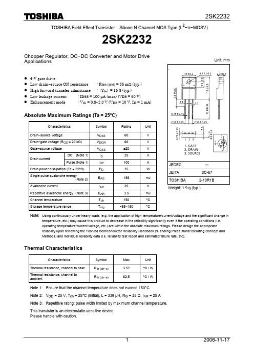
TOSHIBA Field Effect Transistor Silicon N Channel MOS Type (L 2−π−MOSV)2SK2232Chopper Regulator, DC −DC Converter and Motor Drive Applicationsz 4-V gate drivez Low drain −source ON resistance : R DS (ON) = 36 m Ω (typ.) z High forward transfer admittance : |Y fs | = 16 S (typ.)z Low leakage current : I DSS = 100 μA (max) (V DS = 60 V) z Enhancement mode : V th = 0.8~2.0 V (V DS = 10 V, I D = 1 mA)Absolute Maximum Ratings (Ta = 25°C)Characteristics Symbol Rating UnitDrain −source voltageV DSS 60 VDrain −gate voltage (R GS = 20 k Ω) V DGR 60 VGate −source voltage V GSS ±20 V DC (Note 1) I D 25 A Drain currentPulse (Note 1)I DP 100 ADrain power dissipation (Tc = 25°C)P D 35 WSingle pulse avalanche energy(Note 2) E AS 156mJ Avalanche currentI AR 25 A Repetitive avalanche energy (Note 3) E AR 3.5 mJ Channel temperature T ch 150 °C Storage temperature rangeT stg−55~150 °CNote: Using continuously under heavy loads (e.g. the application of high temperature/current/voltage and the significant change intemperature, etc.) may cause this product to decrease in the reliability significantly even if the operating conditions (i.e. operating temperature/current/voltage, etc.) are within the absolute maximum ratings. Please design the appropriate reliability upon reviewing the Toshiba Semiconductor Reliability Handbook (“Handling Precautions”/Derating Concept and Methods) and individual reliability data (i.e. reliability test report and estimated failure rate, etc).Thermal CharacteristicsCharacteristics Symbol Max UnitThermal resistance, channel to case R th (ch −c)3.57°C / W Thermal resistance, channel to ambientR th (ch −a) 62.5°C / WNote 1: Ensure that the channel temperature does not exceed 150°C. Note 2: V DD = 25 V, T ch = 25°C (initial), L = 339 μH, R G = 25 Ω, I AR = 25 A Note 3: Repetitive rating: pulse width limited by maximum channel temperature. This transistor is an electrostatic-sensitive device. Please handle with caution.Unit: mmJEDEC―JEITA SC-67TOSHIBA 2-10R1B Weight: 1.9 g (typ.)Electrical Characteristics (Ta = 25°C)Characteristics SymbolTest ConditionMin Typ. Max Unit Gate leakage current I GSS V GS = ±16 V, V DS = 0 V — — ±10μA Drain cut −off current I DSS V DS = 60 V, V GS = 0 V — — 100μA Drain −source breakdown voltageV (BR) DSSI D = 10 mA, V GS = 0 V 60 — — V Gate threshold voltage V th V DS = 10 V, I D = 1 mA 0.8 — 2.0 V V GS = 4 V, I D = 12 A — 0.057 0.08Drain −source ON resistance R DS (ON)V GS = 10 V, I D = 12 A— 0.036 0.046Ω Forward transfer admittance |Y fs | V DS = 10 V, I D = 12 A1016—SInput capacitanceC iss — 1000 —Reverse transfer capacitance C rss — 200 — Output capacitanceC ossV DS = 10 V, V GS = 0 V, f = 1 MHz — 550 —pF Rise timet r — 20 —Turn −on timet on — 30 —Fall timet f — 55 — Switching timeTurn −off timet off— 130 —nsTotal gate charge (Gate −sourceplus gate–drain) Q g —38 — Gate −source charge Q gs — 25 — Gate −drain (“miller”) chargeQ gdV DD ≈ 48 V, V GS = 10 V, I D = 25 A — 13 —nCSource −Drain Ratings and Characteristics (Ta = 25°C)Characteristics SymbolTest ConditionMin Typ. Max UnitContinuous drain reverse current(Note 1)I DR —— — 25 A Pulse drain reverse current(Note 1) I DRP —— — 100 A Forward voltage (diode) V DSFI DR = 25 A, V GS = 0 V——−1.8VReverse recovery time t rr — 50 — nsReverse recovered chargeQ rr I DR = 25 A, V GS = 0 V, dI DR / dt = 50 A / μs— 35 — μCMarkinglead (Pb)-free package or lead (Pb)-free finish.K2232R G = 25 ΩV DD = 25 V , L = 339 μH⎟⎠⎞⎜⎝⎛−⋅⋅⋅=DD VDSS VDSS AS V B B I L 21E 2RESTRICTIONS ON PRODUCT USE20070701-EN •The information contained herein is subject to change without notice.•TOSHIBA is continually working to improve the quality and reliability of its products. Nevertheless, semiconductor devices in general can malfunction or fail due to their inherent electrical sensitivity and vulnerability to physical stress. It is the responsibility of the buyer, when utilizing TOSHIBA products, to comply with the standards of safety in making a safe design for the entire system, and to avoid situations in which a malfunction or failure of such TOSHIBA products could cause loss of human life, bodily injury or damage to property.In developing your designs, please ensure that TOSHIBA products are used within specified operating ranges as set forth in the most recent TOSHIBA products specifications. Also, please keep in mind the precautions and conditions set forth in the “Handling Guide for Semiconductor Devices,” or “TOSHIBA Semiconductor Reliability Handbook” etc.• The TOSHIBA products listed in this document are intended for usage in general electronics applications (computer, personal equipment, office equipment, measuring equipment, industrial robotics, domestic appliances, etc.).These TOSHIBA products are neither intended nor warranted for usage in equipment that requires extraordinarily high quality and/or reliability or a malfunction or failure of which may cause loss of human life or bodily injury (“Unintended Usage”). Unintended Usage include atomic energy control instruments, airplane or spaceship instruments, transportation instruments, traffic signal instruments, combustion control instruments, medical instruments, all types of safety devices, etc.. Unintended Usage of TOSHIBA products listed in his document shall be made at the customer’s own risk.•The products described in this document shall not be used or embedded to any downstream products of which manufacture, use and/or sale are prohibited under any applicable laws and regulations.• The information contained herein is presented only as a guide for the applications of our products. No responsibility is assumed by TOSHIBA for any infringements of patents or other rights of the third parties which may result from its use. No license is granted by implication or otherwise under any patents or other rights of TOSHIBA or the third parties.• Please contact your sales representative for product-by-product details in this document regarding RoHS compatibility. Please use these products in this document in compliance with all applicable laws and regulations that regulate the inclusion or use of controlled substances. Toshiba assumes no liability for damage or losses occurring as a result of noncompliance with applicable laws and regulations.。
2SK410中文资料

10
1
Ratings 180 ±20 8 120 Hale Waihona Puke 50 –55 to +150
Unit V V A W °C °C
Electrical Characteristics (Ta = 25°C)
Item Power output Drain efficiency Drain to source breakdown voltage Gate to source breakdown voltage Gate to source cutoff voltage Drain current Drain to source saturation voltage Forward transfer admittance Input capacitance Output capacitance Reverse transfer capacitance Power output Power gain Note: 1. Pulse Test Symbol Min PO η V(BR)DSS V(BR)GSS VGS(off) I DSS VDS(on) |yfs| Ciss Coss Crss PO PG 140 — 180 ±20 0.5 — — 0.9 — — — — — Typ 180 80 — — — — 3.8 1.25 440 75 0.5 100 17 Max — — — — 3.0 1.0 6.0 — — — — — — Unit W % V V V mA V S pF pF pF WPEP dB Test conditions VDD = 80 V, f = 28 MHz, I DQ = 0.1 A, Pin = 5 W I D = 10 mA, VGS = 0 I G = ±100 µA, VDS = 0 I D = 1 mA, VDS = 10 V*1 VDS = 140 V, VGS = 0 I D = 4 A, VGS = 10 V*1 I D = 3 A, VDS = 20 V*1 VGS = 5 V, VDS = 0, f = 1 MHz VGS = –5 V, VDS = 50 V, f = 1 MHz VGD = –50 V, f = 1 MHz VDD = 80 V, f = 28 MHz, ∆f = 20 kHz, IMD ≤ –30 dB
2SK1762-E中文资料

VGS = 10 V
0.2 15 V 0.1 0.05 0.5 1 2 5 10 20 50
Gate to Source Voltage VGS (V)
Drain Current ID (A)
Rev.2.00 Sep 07, 2005 page 3 of 6
元器件交易网
80 100
10
Maximum Safe Operation Area
Channel Dissipation Pch (W)
பைடு நூலகம்
30
µs
Drain Current ID (A)
60
10 3 1
PW
DC O pe
10
=
ra
1
0
10
tio
m
m
s
µs
s
40
20
sh ot ) (T c = Operation in this area 25 °C 0.3 is limited by RDS(on) )
元器件交易网
2SK1762
Silicon N Channel MOS FET
REJ03G0969-0200 (Previous: ADE-208-1316) Rev.2.00 Sep 07, 2005
Application
High speed power switching
2 1
Ratings 250 ±30 12 48 12 35 150 –55 to +150
Unit V V A A A W
Tstg
°C °C
Electrical Characteristics
(Ta = 25°C)
Item Drain to source breakdown voltage Gate to source breakdown voltage Gate to source leak current Zero gate voltage drain current Gate to source cutoff voltage Static drain to source on state resistance Forward transfer admittance Input capacitance Output capacitance Reverse transfer capacitance Turn-on delay time Rise time Turn-off delay time Fall time Body to drain diode forward voltage Body to drain diode reverse recovery time Note: 3. Pulse Test Symbol V(BR)DSS V(BR)GSS IGSS IDSS VGS(off) RDS(on) |yfs| Ciss Coss Crss td(on) tr td(off) tf VDF trr Min 250 ±30 — — 2.0 — 5.0 — — — — — — — — — Typ — — — — — 0.23 8.0 1100 440 68 20 65 100 44 1.0 200 Max — — ±10 250 3.0 0.35 — — — — — — — — — — Unit V V µA µA V Ω S pF pF pF ns ns ns ns V ns Test Conditions ID = 10 mA, VGS = 0 IG = ±100 µA, VDS = 0 VGS = ±25 V, VDS = 0 VDS = 200 V, VGS = 0 ID = 1 mA, VDS = 10 V ID = 6 A, VGS = 10 V* ID = 6 A, VDS = 10 V* VDS = 10 V, VGS = 0, f = 1 MHz ID = 6 A, VGS = 10 V, RL = 5 Ω
EK-220说明书中文版

A DIN EN50014
B
C EK220 •
EK220
A-2
1
DINEN60079-14 VDE0165 GB 3836.1 GB 3836.4
A-1
4
1 EK220
(K )
S-GERG88 AGA8 AGA-N1 19
/
1
/ 2Hz
EEPROM 16
2
3
/ /
Calibration Lock Supply Lock
Eq2.T
2
Eq3.T
3
Bin.T
T.Mes
T.Mes=Eq1.T+ Eq2.T Bin.T+ Eq3.T Bin.T2
EK220
Bin.T
22
`EK220
T1Adj T2Adj Prog
Eq3.T 1 2
Prog 1
a)
1
1
1
b)
2
2
2
c) Prog 1
EK220
T.Mes
T.MP
T=T.Mes
T.Mon max T.Mon min
Sel.p
3.9
Eq1.p
1
Eq2.p
2
Eq3.p
3
p.Mes
p.F EK220
Bin.p
19
p.Mes=Eq1.p+ Eq2.p Bin.p+ Eq3.p Bin.p2 EK220
Bin.p
`EK220
p1Adj p2Adj Prog
Eq3.p 1 2
Prog 1
1
1
1
2
2
2
3 Prog 1
- 1、下载文档前请自行甄别文档内容的完整性,平台不提供额外的编辑、内容补充、找答案等附加服务。
- 2、"仅部分预览"的文档,不可在线预览部分如存在完整性等问题,可反馈申请退款(可完整预览的文档不适用该条件!)。
- 3、如文档侵犯您的权益,请联系客服反馈,我们会尽快为您处理(人工客服工作时间:9:00-18:30)。
Drain Current ID (A) Typical Capacitance vs. Drain to Source Voltage
VGS = 0 f = 1 MHz
Reverse Recovery Time trr (ns)
500
Capacitance C (pF)
Outline
RENESAS Package code: PRSS0003AD-A (Package name: TO-220FM)
D G
1. Gate 2. Drain 3. Source
1
2 3
S
Rev.3.00 Sep 20, 2005 page 1 of 6
元器件交易网
40 20 10
Maximum Safe Operation Area
10 µs 10 0 µs
m s
Channel Dissipation Pch (W)
Drain Current ID (A)
30
5 2 1 0.5 0.2 0.1
DC
PW
1
= 10 m s
O
pe
ra
20
(T Operation in c = this area is 25 limited by RDS(on) °
Drain to Source Voltage VDS (V)
Dynamic Input Characteristics
Drain to Source Voltage VDS (V)
200
VGS
Switching Characteristics
20 500
Gate to Source Voltage VGS (V)
tio
n
(1
sh
ot
)
C)
10
Ta = 25°C 2 5 10 20 50 100 200
0
50
100
150
200
Case Temperature TC (°C)
Drain to Source Voltage VDS (V)
Typical Output Characteristics
10 10 V Pulse Test 4V 3.5 V 6 3V 6V 10
Electrical Characteristics
(Ta = 25°C)
Item Drain to source breakdown voltage Gate to source breakdown voltage Gate to source leak current Zero gate voltage drain current Gate to source cutoff voltage Static drain to source on state resistance Forward transfer admittance Input capacitance Output capacitance Reverse transfer capacitance Turn-on delay time Rise time Turn-off delay time Fall time Body to drain diode forward voltage Body to drain diode reverse recovery time Note: 3. Pulse Test Symbol V(BR)DSS V(BR)GSS IGSS IDSS VGS(off) RDS(on) |yfs| Ciss Coss Crss td(on) tr td(off) tf VDF trr Min 120 ±20 — — 1.0 — — 3.0 — — — — — — — — — Typ — — — — — 0.3 0.35 5.0 420 140 35 9 50 140 65 1.35 320 Max — — ±10 250 2.0 0.4 0.55 — — — — — — — — — — Unit V V µA µA V Ω Ω S pF pF pF ns ns ns ns V ns Test conditions ID = 10 mA, VGS = 0 IG = ±100 µA, VDS = 0 VGS = ±16 V, VDS = 0 VDS = 100 V, VGS = 0 ID = 1 mA, VDS = 10 V ID = 4 A, VGS = 10 V*3 ID = 4 A, VGS = 4 V*3 ID = 4 A, VDS = 10 V*3 VDS = 10 V, VGS = 0, f = 1 MHz ID = 4 A, VGS = 10 V, RL = 7.5 Ω
元器件交易网
2SK2202
Silicon N Channel MOS FET
REJ03G1002-0300 (Previous: ADE-208-139) Rev.3.00 Sep 07, 2005
Application
High speed power switching
10 5
VDS = 10 V Pulse Test
0.8
2 1 0.5
0.6
Tc = 75°C 25°C –25°C
0.4
5A 1, 2 A
0.2 0 –40
10 V
0.2 0.1 0.1
0
40
80
120
160
0.2
0.5
1
2
5
10
Case Temperature TC (°C) Body to Drain Diode Reverse Recovery Time
10
Reverse Drain Current IDR (A)
8
Pulse Test
6
4 10 V 2
5V
VGS = 0, –5 V
0
0.4
0.8
1.2
1.6
2.0
Source to Drain Voltage VSD (V) Normalized Transient Thermal Impedance vs. Pulse Width
0.03
0.01 10 µ
0.02 e 1 uls 0.0 tp o h 1s
D=
PW T
100 µ
1m
10 m
100 m
1
10
Pulse Width PW (s)
Switching Time Test Circuit
Vin Monitor D.U.T. RL VDD = 30 V Vout Monitor Vin Vout Vin 10 V 50 Ω 10% 10%
IF = 7 A, VGS = 0 IF = 7 A, VGS = 0, diF / dt = 50 A / µs
Rev.3.00 Sep 20, 2005 page 2 of 6
元器件交易网
2SK2202
Main Characteristics
Power vs. Temperature Derating
500 200 100 50 20 10
Ciss
200 100 50 20 10 0.1 di / dt = 50 A / µs, VGS = 0 Ta = 25°C, Pulse Test 0.2 0.5 1 2 5 10
Coss
Crss
0
10
20
30
40
50
Reverse Drain Current IDR (A)
Normalized Transient Thermal Impedance γS (t)
3 Tc = 25°C D=1 0.5 0.3
0.2
1
0.1
0.1
0.05
θ ch – c(t) = γ s (t) • θ ch – c θ ch – c = 6.25°C/W, Tc = 25°C
PDM PW T
ID = 7 A 120
VDS
Switching Time t (ns)
160
16
200 100 50 20 10 5 3 0.1 0.2 0.5 1
VGS = 10 V VDD = 30 V PW = 2 µs duty < 1 %
td(off) tf tr
12
VDD = 100 V 50 V 25 V VDD = 1er Characteristics
Drain Current ID (A)
Drain Current ID (A)
8
8
VDS = 10 V Pulse Test
6
4
4 Tc = –25°C 25°C 75°C 1 2 3 4 5
2
VGS = 2.5 V
2
0
2
4
6
8
10
0
10 V
0
4
8
12
16
20
0.5
1
2
5
10
20
Gate to Source Voltage VGS (V)
Drain Current ID (A)
Rev.3.00 Sep 20, 2005 page 3 of 6
元器件交易网
2SK2202
Static Drain to Source on State Resistance vs. Temperature
2SK2202
Absolute Maximum Ratings
(Ta = 25°C)
Item Drain to source voltage Gate to source voltage Drain current Drain peak current Body to drain diode reverse drain current Channel dissipation Channel temperature Storage temperature Notes: 1. PW ≤10 µs, duty cycle ≤ 1 % 2. Value at Tc = 25°C Symbol VDSS VGSS ID ID(pulse)*1 IDR Pch*2 Tch Tstg Ratings 120 ±20 7 14 7 20 150 –55 to +150 Unit V V A A A W °C °C