昂宝OB2263中文规格书
OB2263芯片
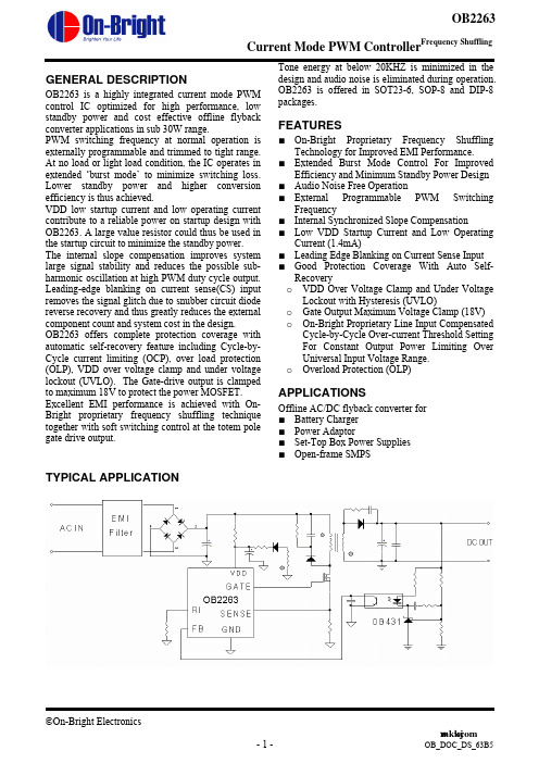
GENERAL DESCRIPTIONOB2263 is a highly integrated current mode PWM control IC optimized for high performance, low standby power and cost effective offline flybackconverter applications in sub 30W range.PWM switching frequency at normal operation is externally programmable and trimmed to tight range. At no load or light load condition, the IC operates in extended ‘burst mode’ to minimize switching loss. Lower standby power and higher conversion efficiency is thus achieved. VDD low startup current and low operating current contribute to a reliable power on startup design with OB2263. A large value resistor could thus be used in the startup circuit to minimize the standby power. The internal slope compensation improves system large signal stability and reduces the possible sub-harmonic oscillation at high PWM duty cycle output. Leading-edge blanking on current sense(CS) input removes the signal glitch due to snubber circuit diode reverse recovery and thus greatly reduces the external component count and system cost in the design. OB2263 offers complete protection coverage with automatic self-recovery feature including Cycle-by-Cycle current limiting (OCP), over load protection (OLP), VDD over voltage clamp and under voltage lockout (UVLO). The Gate-drive output is clamped to maximum 18V to protect the power MOSFET. Excellent EMI performance is achieved with On-Bright proprietary frequency shuffling technique together with soft switching control at the totem pole gate drive output. Tone energy at below 20KHZ is minimized in the design and audio noise is eliminated during operation. OB2263 is offered in SOT23-6, SOP-8 and DIP-8 packages.FEATURES ■ On-Bright Proprietary Frequency Shuffling Technology for Improved EMI Performance.■ Extended Burst Mode Control For Improved Efficiency and Minimum Standby Power Design ■ Audio Noise Free Operation ■ External Programmable PWM Switching Frequency■ Internal Synchronized Slope Compensation■ Low VDD Startup Current and Low Operating Current (1.4mA)■ Leading Edge Blanking on Current Sense Input ■ Good Protection Coverage With Auto Self-Recovery oVDD Over Voltage Clamp and Under Voltage Lockout with Hysteresis (UVLO) o Gate Output Maximum Voltage Clamp (18V) o On-Bright Proprietary Line Input Compensated Cycle-by-Cycle Over-current Threshold Setting For Constant Output Power Limiting OverUniversal Input Voltage Range. o Overload Protection (OLP) APPLICATIONS Offline AC/DC flyback converter for■ Battery Charger ■ Power Adaptor ■ Set-Top Box Power Supplies■ Open-frame SMPSTYPICAL APPLICATIONGENERAL INFORMATIONPin ConfigurationThe OB2263 is offered in SOT23-6, DIP8 and SOP8 packages, shown as below.Ordering Information Part Number DescriptionOB2263MP SOT23-6, Pb-free OB2263AP DIP8, Pb-free OB2263CP SOP8, Pb-freePackage Dissipation RatingPackageR θJA (°C/W)DIP8 90 SOP8 150SOT23-6200Absolute Maximum RatingsParameter Value VDD DC Supply Voltage30 V VDD Zener Clamp VoltageNoteVDD_Clamp+0.1VVDD DC Clamp Current 10 mA V FB Input Voltage -0.3 to 7V V SENSE Input Voltage to Sense Pin-0.3 to 7V V RI Input Voltage to RI Pin -0.3 to 7V Min/Max Operating Junction Temperature T J -20 to 150 o C Min/Max Storage Temperature T stg-55 to 160 o C Note: VDD_Clamp has a nominal value of 34V.Stresses beyond those listed under “absolute maximum ratings” may cause permanent damage to the device. These are stress ratings only, functional operation of the device at these or any other conditions beyond those indicated under “recommended operating conditions” is not implied. Exposure to absolute maximum-rated conditions for extended periods may affect device reliability.Marking InformationTERMINAL ASSIGNMENTSPin Name I/O DescriptionGND PGroundFB I Feedback input pin. The PWM duty cycle is determined by voltage level into this pin and SENSE pin input.RI I Internal Oscillator frequency setting pin. A resistor connected between RI and GND sets the PWM frequency.SENSE I Current sense input pin. Connected to MOSFET current sensing resistor node.VDD P Chip DC power supply pin.GATE O Totem-pole gate drive output for the power MOSFET.RECOMMENDED OPERATING CONDITIONSymbol Parameter MinMaxUnitVDD VDD Supply Voltage 10 to 30 VRI RI Resistor Value 100 KohmT A Operating Ambient Temperature -20 to 85 o CBLOCK DIAGRAMELECTRICAL CHARACTERISTICS(T A = 25O C if not otherwise noted)Symbol Parameter Test Conditions Min Typ Max Unit Supply Voltage (VDD) I_VDD_Startup VDD Start up Current VDD =12.5V, RI=100K Measure Leakage currentinto VDD3 20 uAI_VDD_Ops Operation Current VDD =16V,RI=100Kohm, V FB =3V1.4 mA UVLO(ON) VDD Under Voltage Lockout Enter7.8 8.8 9.8 VUVLO(OFF) VDD Under Voltage Lockout Exit (Recovery)13 14 15 VVDD_Clamp VDD Zener Clamp VoltageI VDD = 5 mA 34 VFeedback Input Section(FB Pin)A VCS PWM Input Gain ΔV FB /ΔV cs2.0 V/V V FB_Open V FB Open Loop Voltage4.8 VI FB _Short FB pin short circuit current Short FB pin to GND and measure current1.2 mAV TH _0D Zero Duty Cycle FB Threshold Voltage VDD = 16V, RI=100Kohm0.75 VV TH _PL Power Limiting FB Threshold Voltage3.7 VT D _PL Power limiting Debounce Time35 mSecZ FB _IN Input Impedance 6 Kohm DC_MAX Maximum Duty Cycle VDD=18V, RI=100Kohm, FB=3V,CS=075 %Current Sense Input(Sense Pin) T_blanking Leading edge blanking timeRI = 100 Kohm 300 nsZ SENSE _IN Input Impedance 40 Kohm T D _OC Over Current Detection andControl DelayVDD = 16V, CS>V TH _OC, FB=3.3V 75 nSecV TH _OC Over CurrentThreshold Voltage at zero Duty CycleFB=3.3V, RI=100 Kohm 0.70 0.75 0.80 V Oscillator F OSC Normal Oscillation FrequencyRI = 100 Kohm 60 65 70 KHZ∆f_TempFrequency Temperature Stability VDD = 16V, RI=100Kohm, T A -20oCto 100 o C5 % ∆f_VDDFrequency Voltage Stability VDD = 12-25V, RI=100Kohm5 % RI_range Operating RI Range 50 100 150 Kohm V_RI_open RI open load voltage 2 VF osc_BM Burst Mode BaseFrequency VDD = 16V, RI =100Kohm22 KHZGate Drive OutputVOL Output Low Level VDD = 16V, Io = -20 mA0.8 V VOH Output High Level VDD = 16V, Io = 20 mA 10 VV_Clamp OutputClampVoltage Level 18VT_r Output Rising Time VDD = 16V, CL = 1nf 220 nSec T_f Output Falling Time VDD = 16V, CL = 1nf 70 nSec Frequency Shuffling∆f_OSC FrequencyModulation range/Base frequencyRI=100K -33%f_shuffling Shuffling Frequency RI=100K 64 HZUVLO(ON) vs Temp8.08.28.48.68.89.0-20104070100130Temp(C)U V L O (O N ) (V )OPERATION DESCRIPTIONThe OB2263 is a highly integrated PWM controller IC optimized for offline flyback converter applications in sub 30W power range. The extended burst mode control greatly reduces the standby power consumption and helps the design easily meet the international power conservation requirements.•Startup Current and Start up Control Startup current of OB2263 is designed to be very low so that VDD could be charged up above UVLO threshold level and device starts up quickly. A large value startup resistor can therefore be used to minimize the power loss yet provides reliable startup in application. For AC/DC adaptor with universal input range design, a 2 MΩ, 1/8 W startup resistor could be used together with a VDD capacitor to provide a fast startup and low power dissipation solution.•Operating CurrentThe Operating current of OB2263 is low at 1.4mA. Good efficiency is achieved with OB2263 low operating current together with extended burst mode control features.•Frequency shuffling for EMI improvement The frequency Shuffling/jittering (switching frequency modulation) is implemented in OB2263. The oscillation frequency is modulated with a random source so that the tone energy is spread out. The spread spectrum minimizes the conduction band EMI and therefore reduces system design challenge.•Extended Burst Mode OperationAt zero load or light load condition, majority of the power dissipation in a switching mode power supply is from switching loss on the MOSFET transistor, the core loss of the transformer and the loss on the snubber circuit. The magnitude of power loss is in proportion to the number of switching events within a fixed period of time. Reducing switching events leads to the reduction on the power loss and thus conserves the energy.OB2263 self adjusts the switching mode according to the loading condition. At from no load to light/medium load condition, the FB input drops below burst mode threshold level. Device enters Burst Mode control. The Gate drive output switches only when VDD voltage drops below a preset level and FB input is active to output an on state. Otherwise the gate drive remains at off state to minimize the switching loss and reduces the standby power consumption to the greatest extend. The frequency control also eliminates the audio noise at any loading conditions.•Oscillator OperationA resistor connected between RI and GND sets the constant current source to charge/discharge the internal cap and thus the PWM oscillator frequency is determined. The relationship between RI and switching frequency follows the below equation within the specified RI in Kohm range at nominal loading operational condition.)()(6500KhzKohmRIFOSC=•Current Sensing and Leading Edge Blanking Cycle-by-Cycle current limiting is offered in OB2263 current mode PWM control. The switch current is detected by a sense resistor into the sense pin. An internal leading edge blanking circuit chops off the sense voltage spike at initial MOSFET on state due to Snubber diode reverse recovery so that the external RC filtering on sense input is no longer required. The current limit comparator is disabled and thus cannot turn off the external MOSFET during the blanking period. PWM duty cycle is determined by the current sense input voltage and the FB input voltage.•Internal Synchronized Slope Compensation Built-in slope compensation circuit adds voltage ramp onto the current sense input voltage for PWM generation. This greatly improves the close loop stability at CCM and prevents the sub-harmonic oscillation and thus reduces the output ripple voltage.•Gate DriveOB2263 Gate is connected to an external MOSFET gate for power switch control. Too weak the gate drive strength results in higher conduction and switch loss of MOSFET while too strong gate drive output compromises the EMI.A good tradeoff is achieved through the built-in totem pole gate design with right output strength and dead time control. The low idle loss and good EMI system design is easier to achieve with this dedicated control scheme. An internal 18V clamp is added for MOSFET gate protection at higher than expected VDD input.Current Mode PWM Controllerm kw k c om• Protection ControlsGood power supply system reliability is achieved with its rich protection features including Cycle-by-Cycle current limiting (OCP), Over Load Protection (OLP) and over voltage clamp, Under Voltage Lockout on VDD (UVLO).With On-Bright Proprietary technology, the OCP threshold tracks PWM Duty cycles and is line voltage compensated to achieve constant output power limit over the universal input voltage range with recommended reference design.At overload condition when FB input voltage exceeds power limit threshold value for more than TD_PL, control circuit reacts to shut down the output power MOSFET. Device restarts when VDD voltage drops below UVLO limit.VDD is supplied by transformer auxiliary winding output. It is clamped when VDD is higher than threshold value. The power MOSFET is shut down when VDD drops below UVLO limit and device enters power on start-up sequence thereafter.PACKAGE MECHANICAL DATASOT23-68-Pin Plastic DIP8-Pin Plastic SOPIMPORTANT NOTICERIGHT TO MAKE CHANGESOn-Bright Electronics Corp. reserves the right to make corrections, modifications, enhancements, improvements and other changes to its products and services at any time and to discontinue any product or service without notice. Customers should obtain the latest relevant information before placing orders and should verify that such information is current and complete.WARRANTY INFORMATIONOn-Bright Electronics Corp. warrants performance of its hardware products to the specifications applicable at the time of sale in accordance with its standard warranty. Testing and other quality control techniques are used to the extent it deems necessary to support this warranty. Except where mandated by government requirements, testing of all parameters of each product is not necessarily performed.On-Bright Electronics Corp. assumes no liability for application assistance or customer product design. Customers are responsible for their products and applications using On-Bright’s components, data sheet and application notes. To minimize the risks associated with customer products and applications, customers should provide adequate design and operating safeguards.LIFE SUPPORTOn-Bright Electronics Corp.’s products are not designed to be used as components in devices intended to support or sustain human life. On-bright Electronics Corp. will not be held liable for any damages or claims resulting from the use of its products in medical applications.MILITARYOn-Bright Electronics Corp.’s products are not designed for use in military applications. On-Bright Electronics Corp. will not be held liable for any damages or claims resulting from the use of its products in military applications.。
ob6683cgpa规格书

ob6683cgpa规格书英文回答:OB6683CGPA Specification.Introduction:The OB6683CGPA specification outlines the requirements and standards for the OB6683CGPA product. Thisspecification aims to provide a detailed description of the product's features, functionality, and performance expectations. In this response, I will discuss the key aspects of the OB6683CGPA specification and provide examples to illustrate its application.Product Features:The OB6683CGPA is a versatile and high-performance device that offers a range of features to meet the needs of users. It is equipped with advanced technology andinnovative design elements. Some of its notable features include:1. High-resolution display: The OB6683CGPA boasts a vibrant and sharp display, allowing users to enjoy crystal-clear visuals and an immersive viewing experience.2. Powerful processor: With a state-of-the-art processor, the OB6683CGPA delivers lightning-fast performance, enabling seamless multitasking and smooth operation of resource-intensive applications.3. Extensive storage capacity: The OB6683CGPA offers ample storage space, allowing users to store a large amount of data, including photos, videos, and documents, without worrying about running out of space.4. Advanced camera system: The OB6683CGPA is equipped with a high-quality camera system, enabling users to capture stunning photos and videos with exceptional clarity and detail.Performance Expectations:The OB6683CGPA is designed to deliver exceptional performance across various tasks and applications. Its powerful hardware and optimized software ensure smooth and efficient operation. Some performance expectations for the OB6683CGPA include:1. Fast and responsive user interface: The OB6683CGPA provides a seamless user experience with its quick and responsive interface. Users can navigate through menus, open applications, and perform tasks without any lag or delay.2. Smooth gaming experience: The OB6683CGPA is capable of handling graphically demanding games with ease. Users can enjoy a smooth and immersive gaming experience without experiencing any frame drops or stuttering.3. Efficient multitasking: The OB6683CGPA allows users to run multiple applications simultaneously without compromising performance. Users can switch between appsseamlessly and enjoy a seamless multitasking experience.4. Long battery life: The OB6683CGPA is equipped with a high-capacity battery that provides extended usage time. Users can enjoy using the device for extended periodswithout worrying about frequent recharging.中文回答:OB6683CGPA规格书。
开关环路设计与计算

开关电源系统基本组成部分(Voltage Mode PWM System)开关电源环路分析和设计流程开关电源环路的小信号传函FlybackTL431Power StageFlyback PWM Stage右半平面零点PWM Stage()t d)+考虑斜率补偿后的考虑斜率补偿后的考虑斜率补偿后的考虑斜率补偿后的考虑斜率补偿后的DCM模式下电流模式与电压模式的直观理解()(O V D V D =−−1()(v d V V vI L 1ˆˆˆ−−+=()D I I L O −=1dI i L O ˆˆ−=电压模式的信号流程图(siˆ电流模式的信号流程图零极点对环路稳定性的影响及环路带宽选择标准环路的补偿方法把控制带宽拉低,在功率部分或加有其他补偿的部分相位达环路的补偿方法常用的补偿方式.补偿网络产生一个s=0(DC)极点,而且通常所以补偿网络需补偿网络的高频极点抵消输出滤波电容的ESR零点。
环路的补偿方法复杂,适用于输出带LC滤波的拓扑结构中.补偿网络产生一个s=0(DC)极点,以及两个零点和两个极点,反激变换器反馈回路的设计采用补偿方法Power Stage GainOB2263 控制芯片内部模块图OB2263OB2263基于OB2263的基于OB2263的基于OB2263的基于OB2263的5) 确定EA补偿网络的零点和极点的位置基于OB2263的基于OB2263的附录: 431及其补偿网络传函的推导6KR I v ⋅−=Thank you Any Questions?。
因为OB2263直接驱动时只适合做到36W左右为了降低成本很多
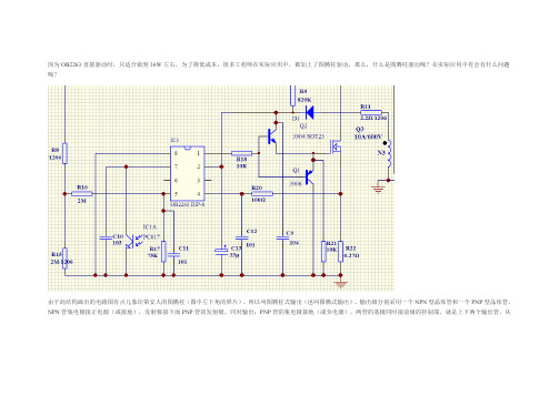
因为OB2263直接驱动时,只适合做到36W左右,为了降低成本,很多工程师在实际应用中,都加上了图腾柱驱动,那么,什么是图腾柱驱动呢?在实际应用中有会有什么问题呢?由于此结构画出的电路图有点儿象印第安人的图腾柱(图中左下角的照片),所以叫图腾柱式输出(也叫图腾式输出)。
输出级分别采用一个NPN型晶体管和一个PNP型晶体管。
NPN管集电极接正电源(或接地),发射极接下面PNP管的发射极,同时输出;PNP管的集电极接地(或负电源)。
两管的基极同时接前级的控制端。
就是上下两个输出管,从直流角度看是串联,而从交流看是并联,两管发射极连接处为输出端,实际是一对射极跟随器。
追随输入电平,上管导通、下管截止输出高电平,下管导通、上管截止输出低电平,如果上下两管均截止则输出为高阻态。
在开关电源中,类似的电路常称为“半桥”。
1.不就是OUT高位时,上三极管导通,下三极管关断,Rgate接上Vdrv,MOS开通,OUT低位时,反过来,Rgate接地,MOS关断。
2.输出极采用一个上电阻接一个NPN型晶体管的集电极,这个管子的发射极接下面管子的集电极同时输出;下管的发射极接地.两管的基极分别接前级的控制.就是上下两个输出管,从直流角度看是串联,两管联接处为输出端.上管导通下管截止输出高电平,下管导通上管截止输出低电平,如果电路逻辑可以上下两管均截止则输出为高阻态.其实也是用NPN和PNP管子的搭配使用,当上升沿的时候NPN工作打开,当下降沿的时候PNP工作关闭,依次循环。
3.这个电路看似简单,其实用起来要考虑的还比较多,简单谈谈个人的看法,先声明一下,只是随手总结,可能有不对或不足之处,1)首先要确定的是你需要多少的驱动能力?要驱动的负载(一般可认为是功率管)有多少?以MOSFET为例,驱动其实就是对MOS的门级电容的充放电,这就要考虑你有几个MOS并联,门级电容有多大?MOS的Rg 有多大,加上驱动回路寄生电感等,其实就是一个LRC串联回路。
OB2263

GENERAL DESCRIPTIONOB2263 is a highly integrated current mode PWM control IC optimized for high performance, low standby power and cost effective offline flybackconverter applications in sub 30W range.PWM switching frequency at normal operation is externally programmable and trimmed to tight range.At no load or light load condition, the IC operates in extended ‘burst mode’ to minimize switching loss.Lower standby power and higher conversion efficiency is thus achieved.VDD low startup current and low operating currentcontribute to a reliable power on startup design with OB2263. A large value resistor could thus be used in the startup circuit to minimize the standby power.The internal slope compensation improves system large signal stability and reduces the possible sub-harmonic oscillation at high PWM duty cycle output.Leading-edge blanking on current sense(CS) inputremoves the signal glitch due to snubber circuit diodereverse recovery and thus greatly reduces the externalcomponent count and system cost in the design.OB2263 offers complete protection coverage withautomatic self-recovery feature including Cycle-by-Cycle current limiting (OCP), over load protection(OLP), VDD over voltage clamp and under voltagelockout (UVLO). The Gate-drive output is clamped to maximum 18V to protect the power MOSFET. Excellent EMI performance is achieved with On-Bright proprietary frequency shuffling technique together with soft switching control at the totem pole gate drive output. Tone energy at below 20KHZ is minimized in the design and audio noise is eliminated during operation. OB2263 is offered in SOT23-6, SOP-8 and DIP-8 packages.FEATURES ■ On-Bright Proprietary Frequency ShufflingTechnology for Improved EMI Performance. ■ Extended Burst Mode Control For ImprovedEfficiency and Minimum Standby Power Design ■ Audio Noise Free Operation■ External Programmable PWM Switching Frequency ■ Internal Synchronized Slope Compensation■ Low VDD Startup Current and Low OperatingCurrent (1.4mA) ■ Leading Edge Blanking on Current Sense Input■ Good Protection Coverage With Auto Self-Recovery o VDD Over Voltage Clamp and Under Voltage Lockout with Hysteresis (UVLO) o Gate Output Maximum Voltage Clamp (18V) o On-Bright Proprietary Line Input Compensated Cycle-by-Cycle Over-current Threshold Setting For Constant Output Power Limiting OverUniversal Input Voltage Range. o Overload Protection (OLP) APPLICATIONS Offline AC/DC flyback converter for■ Battery Charger ■ Power Adaptor ■ Set-Top Box Power Supplies■ Open-frame SMPSTYPICAL APPLICATIONGENERAL INFORMATIONPin ConfigurationThe OB2263 is offered in SOT23-6, DIP8 and SOP8 packages, shown as below.Ordering Information Part Number DescriptionOB2263MP SOT23-6, Pb-free OB2263AP DIP8, Pb-free OB2263CP SOP8, Pb-freePackage Dissipation RatingPackageR θJA (°C/W)DIP8 90 SOP8 150SOT23-6200Absolute Maximum RatingsParameter Value VDD DC Supply Voltage 30 VVDD Zener Clamp VoltageNoteVDD_Clamp+0.1VVDD DC Clamp Current 10 mA V FB Input Voltage -0.3 to 7V V SENSE Input Voltage to Sense Pin-0.3 to 7V V RI Input Voltage to RI Pin -0.3 to 7V Min/Max Operating Junction Temperature T J -20 to 150 o C Min/Max Storage Temperature T stg-55 to 160 o C Note: VDD_Clamp has a nominal value of 34V.Stresses beyond those listed under “absolute maximum ratings” may cause permanent damage to the device. These are stress ratings only, functional operation of the device at these or any other conditions beyond those indicated under “recommended operating conditions” is not implied. Exposure to absolute maximum-rated conditions for extended periods may affect device reliability.Marking InformationTERMINAL ASSIGNMENTSPin Name I/O DescriptionGroundGND PFB I Feedback input pin. The PWM duty cycle is determined by voltage level into this pin and SENSE pin input.RI I Internal Oscillator frequency setting pin. A resistor connected between RI and GND sets the PWM frequency.SENSE I Current sense input pin. Connected to MOSFET current sensing resistor node.VDD P Chip DC power supply pin.GATE O Totem-pole gate drive output for the power MOSFET.RECOMMENDED OPERATING CONDITIONUnit Symbol Parameter MinMaxVDD VDD Supply Voltage 10 to 30 VRI RI Resistor Value 100 KohmT A Operating Ambient Temperature -20 to 85 o CBLOCK DIAGRAMELECTRICAL CHARACTERISTICS(T A = 25O C if not otherwise noted)Symbol Parameter Test Conditions Min Typ Max Unit Supply Voltage (VDD) I_VDD_Startup VDD Start up Current VDD =12.5V, RI=100K Measure Leakage currentinto VDD3 20 uAI_VDD_Ops Operation Current VDD =16V,RI=100Kohm, V FB =3V1.4 mA UVLO(ON) VDD Under Voltage Lockout Enter7.8 8.8 9.8 VUVLO(OFF) VDD Under Voltage Lockout Exit (Recovery)13 14 15 VVDD_Clamp VDD Zener Clamp VoltageI VDD = 5 mA 34 VFeedback Input Section(FB Pin)A VCS PWM Input Gain ΔV FB /ΔV cs2.0 V/V V FB_Open V FB Open Loop Voltage4.8 VI FB _Short FB pin short circuit current Short FB pin to GND and measure current1.2 mAV TH _0D Zero Duty Cycle FB Threshold Voltage VDD = 16V, RI=100Kohm0.75 VV TH _PL Power Limiting FB Threshold Voltage3.7 VT D _PL Power limiting Debounce Time35 mSecZ FB _IN Input Impedance 6 Kohm DC_MAX Maximum Duty Cycle VDD=18V, RI=100Kohm, FB=3V,CS=075 %Current Sense Input(Sense Pin) T_blanking Leading edge blanking timeRI = 100 Kohm 300 nsZ SENSE _IN Input Impedance 40 Kohm T D _OC Over Current Detection andControl DelayVDD = 16V, CS>V TH _OC, FB=3.3V 75 nSecV TH _OC Over CurrentThreshold Voltage at zero Duty CycleFB=3.3V, RI=100 Kohm 0.70 0.75 0.80 V Oscillator F OSC Normal Oscillation FrequencyRI = 100 Kohm 60 65 70 KHZ∆f_TempFrequency Temperature Stability VDD = 16V, RI=100Kohm, T A -20oCto 100 o C5 % ∆f_VDDFrequency Voltage Stability VDD = 12-25V, RI=100Kohm5 % RI_range Operating RI Range 50 100 150 Kohm V_RI_open RI open load voltage 2 VF osc_BM Burst Mode BaseFrequency VDD = 16V, RI =100Kohm22 KHZGate Drive OutputVOL Output Low Level VDD = 16V, Io = -20 mA0.8 V VOH Output High Level VDD = 16V, Io = 20 mA 10 VV_Clamp OutputClampVoltage Level 18VT_r Output Rising Time VDD = 16V, CL = 1nf 220 nSec T_f Output Falling Time VDD = 16V, CL = 1nf 70 nSec Frequency Shuffling∆f_OSC FrequencyModulation range/Base frequencyRI=100K -33%f_shuffling Shuffling Frequency RI=100K 64 HZUVLO(ON) vs Temp8.08.28.48.68.89.0-20104070100130Temp(C)U V L O (O N ) (V )OPERATION DESCRIPTIONThe OB2263 is a highly integrated PWM controller IC optimized for offline flyback converter applications in sub 30W power range. The extended burst mode control greatly reduces the standby power consumption and helps the design easily meet the international power conservation requirements.•Startup Current and Start up Control Startup current of OB2263 is designed to be very low so that VDD could be charged up above UVLO threshold level and device starts up quickly. A large value startup resistor can therefore be used to minimize the power loss yet provides reliable startup in application. For AC/DC adaptor with universal input range design, a 2 MΩ, 1/8 W startup resistor could be used together with a VDD capacitor to provide a fast startup and low power dissipation solution.•Operating CurrentThe Operating current of OB2263 is low at 1.4mA. Good efficiency is achieved with OB2263 low operating current together with extended burst mode control features.•Frequency shuffling for EMI improvement The frequency Shuffling/jittering (switching frequency modulation) is implemented in OB2263. The oscillation frequency is modulated with a random source so that the tone energy is spread out. The spread spectrum minimizes the conduction band EMI and therefore reduces system design challenge.•Extended Burst Mode OperationAt zero load or light load condition, majority of the power dissipation in a switching mode power supply is from switching loss on the MOSFET transistor, the core loss of the transformer and the loss on the snubber circuit. The magnitude of power loss is in proportion to the number of switching events within a fixed period of time. Reducing switching events leads to the reduction on the power loss and thus conserves the energy.OB2263 self adjusts the switching mode according to the loading condition. At from no load to light/medium load condition, the FB input drops below burst mode threshold level. Device enters Burst Mode control. The Gate drive output switches only when VDD voltage drops below a preset level and FB input is active to output an on state. Otherwise the gate drive remains at off state to minimize the switching loss and reduces the standby power consumption to the greatest extend. The frequency control also eliminates the audio noise at any loading conditions.•Oscillator OperationA resistor connected between RI and GND sets the constant current source to charge/discharge the internal cap and thus the PWM oscillator frequency is determined. The relationship between RI and switching frequency follows the below equation within the specified RI in Kohm range at nominal loading operational condition.)()(6500KhzKohmRIFOSC=•Current Sensing and Leading Edge Blanking Cycle-by-Cycle current limiting is offered in OB2263 current mode PWM control. The switch current is detected by a sense resistor into the sense pin. An internal leading edge blanking circuit chops off the sense voltage spike at initial MOSFET on state due to Snubber diode reverse recovery so that the external RC filtering on sense input is no longer required. The current limit comparator is disabled and thus cannot turn off the external MOSFET during the blanking period. PWM duty cycle is determined by the current sense input voltage and the FB input voltage.•Internal Synchronized Slope Compensation Built-in slope compensation circuit adds voltage ramp onto the current sense input voltage for PWM generation. This greatly improves the close loop stability at CCM and prevents the sub-harmonic oscillation and thus reduces the output ripple voltage.•Gate DriveOB2263 Gate is connected to an external MOSFET gate for power switch control. Too weak the gate drive strength results in higher conduction and switch loss of MOSFET while too strong gate drive output compromises the EMI.A good tradeoff is achieved through the built-in totem pole gate design with right output strength and dead time control. The low idle loss and good EMI system design is easier to achieve with this dedicated control scheme. An internal 18V clamp is added for MOSFET gate protection at higher than expected VDD input.•Protection ControlsGood power supply system reliability is achieved with its rich protection features including Cycle-by-Cycle current limiting (OCP), Over Load Protection (OLP) and over voltage clamp, Under Voltage Lockout on VDD (UVLO).With On-Bright Proprietary technology, the OCP threshold tracks PWM Duty cycles and is line voltage compensated to achieve constant output power limit over the universal input voltage range with recommended reference design. At overload condition when FB input voltage exceeds power limit threshold value for more than TD_PL, control circuit reacts to shut down the output power MOSFET. Device restarts when VDD voltage drops below UVLO limit.VDD is supplied by transformer auxiliary winding output. It is clamped when VDD is higher than threshold value. The power MOSFET is shut down when VDD drops below UVLO limit and device enters power on start-up sequence thereafter.PACKAGE MECHANICAL DATA SOT23-68-Pin Plastic DIP8-Pin Plastic SOP。
昴宝OB2263PDF详细文档
Current Mode PWM ControllerFrequency Shuffling
Tone energy at below 20KHZ is minimized in the
GENERAL DESCRIPTION
design and audio noise is eliminated during operation.
OB2263AP
DIP8, Pb-free
The OB2263 is offered in SOT23-6, DIP8 and SOP8
OB2263CP
SOP8, Pb-free
packages, shown as below.
Package Dissipation Rating
Package
RθJA
Cycle-by-Cycle Over-current Threshold Setting
rFor Constant Output Power Limiting Over aUniversal Input Voltage Range. Cho Overload Protection (OLP)
lockout (UVLO). The Gate-drive output is clamped to maximum 18V to protect the power MOSFET.
-0.3 to 7V -20 to 150 oC
r Temperature TJ a Min/Max Storage Temperature -55 to 160 oC
hTstg CNote: Stresses beyond those listed under “absolute maximum
开关电源芯片HT2263、2269的基本运用(1)

设备,电子产品,照明产品等等,目前在中国市 场上做得最多的是照明产品,包括节能灯(CFL, 灯具(RLF),交通信号灯和出口指示灯。 目前全球计有七个国家参与美国环保署推动 的能源之星计划,分别为美国、加拿大、日本、 台湾、澳洲、新西兰、欧盟。
对于小型开关电源的标准如下:
Foxit PDF Document
二、 开关电源的概念 开关电源就是用通过电路控制开关管进行 高速的导通与截止.将直流电转换为高频率的交 流电提供给变压器进行变压,从而产生所需要的 一组或多组电压的电源。 1、开关电源主要有以下特点: (1).体积小、重量轻:由于没有工频变压器, 所以体积和重量只有线性电源的20~30%。 (2).功耗小、效率高:功率晶体管工作在开关 状态,所以晶体管上的功耗小,转 化效率高, 一般为60~70%,而线性电电源只有30~40%。
五、我们公司的AC-DC产品
产品型号 SP3706 SP3842 SP3843 SP7500 TL494 VIPER22A HT202 HT203 HT2262 HT2263 HT2268 HT2269 功能 PWM PWM PWM PWM PWM PWM+MOSFET PWM+三级管 PWM+三级管 PWM PWM PWM PWM Vin(AC) 85-264V 85-264V 85-264V 85-264V 85-264V 85-264V 85-264V 85-264V 85-264V 85-264V 85-264V 85-264V Vdd 4.8-5.3V 10-30V 10-30V 7-40V 7-40V 9-38V 4.8-9V 4.8-10V 11-30V 11-30V 12-23V 12-23V 启动电流 70uA 0.5mA 0.5mA 1mA 2.4mA 2.4mA 3uA 3uA 6.5uA 6.5uA 输出最大电 振荡频率 流/功率 10W 1A 1A 200mA 200mA 20W 5W 18W 30W 30W 100W 100W Adaptive 500KHz 500KHz 300KHz 300KHz 60KHz 66KHz 66KHz 65KHz 65KHz 65KHz 65KHz 封装 SOIC-8 SOIC-8 DIP8 SOIC-8 DIP8 SOIC-16 DIP-16 SOIC-16 DIP-16 DIP-8 DIP-8 DIP-8 SOT23-6 SOT23-6 SOIC-8 DIP8 SOIC-8 DIP8 备注
昂宝-OB2535规格书
MBr i d e ch n ol o gy Co .,Lt d .OB2535High Precision CC/CV Primary-Side PWM Power SwitchGENERAL DESCRIPTIONOB2535 is a high performance offline PWM Power switch for low power AC/DC charger and adaptor applications. It operates in primary-side sensing and regulation. Consequently, opto-coupler and TL431 could be eliminated. Proprietary Constant Voltage (CV) and Constant Current (CC) control is integrated as shown in the figure below.In CC control, the current and output power setting can be adjusted externally by the sense resistor Rs at CS pin. In CV control, multi-mode operations are utilized to achieve high performance and high efficiency. In addition, good load regulation is achieved by the built-in cable drop compensation. Device operates in PFM in CC mode as well at large load condition and it operates in PWM with frequency reduction at light/medium load.OB2535 offers power on soft start control and protection coverage with auto-recovery features including Cycle-by-Cycle current limiting, VDD OVP, VDD clamp and UVLO. Excellent EMI performance is achieved with On-Bright proprietary frequency shuffling technique.High precision constant voltage (CV) and constant current (CC) can be achieved by OB2535. .Fig.1. Typical CC/CV CurveFEATURES5% Constant Voltage Regulation, 5% ConstantCurrent Regulation at Universal AC input Primary-side Sensing and Regulation WithoutTL431 and Opto-couplerProgrammable CV and CC RegulationAdjustable Constant Current and Output PowerSettingBuilt-in Secondary Constant Current Controlwith Primary Side FeedbackBuilt-in Adaptive Current Peak Regulation Built-in Primary winding inductancecompensationProgrammable Cable drop Compensation Power on Soft-startBuilt-in Leading Edge Blanking (LEB) Cycle-by-Cycle Current LimitingVDD Under Voltage Lockout with Hysteresis(UVLO) VDD OVP VDD ClampAPPLICATIONSLow Power AC/DC offline SMPS for Cell Phone ChargerDigital Cameras Charger Small Power AdaptorAuxiliary Power for PC, TV etc. Linear Regulator/RCC ReplacementOB2535 is offered in SOP8 package.TYPICAL APPLICATIONM icr oBge Te ch n ol o gy Co .,Lt d .OB2535High Precision CC/CV Primary-Side PWM Power SwitchGENERAL INFORMATIONPin ConfigurationThe pin map is shown as below for SOP8VDD COMP INVCSGND GNDOrdering Information Part Number Description OB2535CP SOP8, Pb-free, Tube OB2535CPA SOP8, Pb-free, T&RPackage Dissipation Rating Package R θJA (℃/W) SOP8 90Note: Drain Pin Connected 100mm 2 PCB copper clad.Absolute Maximum RatingsParameter Value Drain Voltage (off state) -0.3V to Bvdss VDD Voltage -0.3 to V DD _clamp VDD Zener Clamp Continuous Current 10 mA COMP Voltage -0.3 to 7V CS Input Voltage -0.3 to 7V INV Input Voltage -0.3 to 7V Min/Max Operating Junction Temperature T J -20 to 150 o C Min/Max Storage Temperature T stg -55 to 150 o C Lead Temperature (Soldering, 10secs) 260 o CNote: Stresses beyond those listed under “absolute maximum ratings” may cause permanent damage to the device. These are stress ratings only, functional operation of the device at these or any other conditions beyond those indicated under “recommended operating conditions” is not implied. Exposure to absolute maximum-rated conditions for extended periods may affect device reliability.M ic r oBr id ge Te ch nol o gy Co .,Lt d .OB2535High Precision CC/CV Primary-Side PWM Power SwitchMarking InformationOB2535CP YWWSC:SOP8 Package P:Pb-free Package Y:Year Code(0-9)WW:Week Code(01-52)S:Internal Code(Optional)TERMINAL ASSIGNMENTSPin Num Pin Name I/O Description 1 VDD P Power Supply 2 COMP I Loop Compensation for CV Stability3 INV I The voltage feedback from auxiliary winding. Connected to resistor dividerfrom auxiliary winding reflecting output voltage. PWM duty cycle isdetermined by EA output and current sense signal at pin 4.4 CS I Current sense input5/6 DRAIN OHV MOSFET Drain Pin. The Drain pin is connected to the primary lead ofthe transformer7/8 GND P GroundOUTPUT POWER TABLE230VAC±15% 85-264VAC Product Adapter 1 Adapter 1OB2535 6W 5WNotes:1.Maximum practical continuous power in an Adapter design with sufficient drain pattern as a heat sink, at 50℃ ambient.M ic r oBr i d geBLOCK DIAGRAMM ic r oBr i d ge Te ch n ol o gy Co .,Lt d .ELECTRICAL CHARACTERISTICS(T A = 25O C, VDD=VDDG=16V, if not otherwise noted)Symbol Parameter Test Conditions Min Typ Max UnitSupply Voltage (VDD) Section I DD ST Standby Current VDD=13V5 20uA I DD op Operation CurrentOperation supply current INV=2V, CS=0V,VDD=VDDG=20V- 2.5 3.5 mAUVLO(ON) VDD Under Voltage Lockout Enter VDD falling 7.5 8.5 10V UVLO(OFF) VDD Under Voltage Lockout Exit VDD rsing13.5 14.5 16.0V V DD _clamp Maximum VDD operationvoltageI DD =10mA30.5 32.5 34.5V OVPOver voltage protection ThresholdRamp VDD until gate shut down27.5 29.5 31.5V Current Sense Input SectionTLEB LEB time540 ns Vth_oc Over current threshold870 900 930 mVTd_oc OCP Propagation delay150 ns Z SENSE _IN Input Impedance50 KohmT_ssSoft start time10msFrequency SectionFreq_Max Note 1 IC Maximum frequency66 72 78 KHzFreq_NomSystem Nominal switch frequency60KHzFreq_startup INV =0V, Comp =5V 14 KHz △f/FreqFrequency shuffling range+/-4% Error Amplifier section Vref_EA Reference voltage for EA 1.972 2.03 V GainDC gain of EA60 dB I_COMP_MAXMax. Cable compensationcurrentINV=2V, Comp=0V42uAPower MOSFET Section BVdss MOSFET Drain-Source Breakdown Voltage 600 V RdsonOn ResistanceStatic, Id=0.4A1215ΏNote:1. Freq_Max indicates IC internal maximum clock frequency. In system application, the maximum operation frequency of 60Khz nominal occurs at maximum output power or the transition point from CV to CC.M ic r oBr i d g e T en t CHARACTERIZATION PLOTSM ic r oBr i d ge Te c.,Lt d .OPERATION DESCRIPTIONOB2535 is a cost effective PWM power switch optimized for off-line low power AC/DC applications including battery chargers and adaptors. It operates in primary side sensing and regulation, thus opto-coupler and TL431 are not required. Proprietary built-in CV and CC control can achieve high precision CC/CV control meeting most adaptor and charger application requirements.z Startup Current and Start up ControlStartup current of OB2535 is designed to be very low so that VDD could be charged up above UVLO threshold and starts up quickly. A large value startup resistor can therefore be used to minimize the power loss in application.z Operating CurrentThe Operating current of OB2535 is as low as 2.5mA. Good efficiency is achieved with the low operating current together with ‘Muti-mode’ control features.z Soft StartOB2535 features an internal soft start to minimize the component electrical over-stress during power on startup. As soon as VDD reaches UVLO (OFF), the control algorithm will ramp peak current voltage threshold gradually from nearly zero to normal setting of 0.90V. Every restart is a soft start.z CC/CV OperationOB2535 is designed to produce good CC/CV control characteristic as shown in the Fig. 1.In charger applications, a discharged battery charging starts in the CC portion of the curve until it is nearly full charged and smoothly switches to operate in CV portion of the curve.In an AC/DC adapter, the normal operation occurs only on the CV portion of the curve. The CC portion provides output current limiting. In CV operation, the output voltage is regulated through the primary side control. In CC operation mode, OB2535 will regulate the output current constant regardless of the output voltage drop.z Principle of OperationTo support OB2535 proprietary CC/CV control, system needs to be designed in DCM mode for flyback system (Refer to Typical Application Diagram on page1).In the DCM flyback converter, the output voltage can be sensed via the auxiliary winding. During MOSFET turn-on time, the load current is supplied from the output filter capacitor Co. The current inthe primary winding ramps up. When MOSFET turns off, the primary current transfers to the secondary at the amplitude ofP SPS I N N I ⋅=(1) The auxiliary voltage reflects the output voltage as shown in fig.2 and it is given by)(V V N N V O SAUXAUX Δ+⋅=(2) Where ΔV indicates the drop voltage of the output Diode.Fig.2. Auxiliary voltage waveformVia a resistor divider connected between the auxiliary winding and INV (pin 3), the auxiliary voltage is sampled at the end of the de-magnetization and it is hold until the next sampling. The sampled voltage is compared with Vref (2.0V) and the error is amplified. The error amplifier output COMP reflects the load condition and controls the PWM switching frequency to regulate the output voltage, thus constant output voltage can be achieved.When sampled voltage is below Vref and the error amplifier output COMP reaches its maximum, the switching frequency is controlled by the sampled voltage thus the output voltage to regulate the output current, thus the constant output current can be achieved.z Adjustable CC point and Output PowerIn OB2535, the CC point and maximumoutput power can be externally adjusted by external current sense resistor Rs at CS pin as illustrated in Typical Application Diagram. The output power is adjusted through CC point change. The larger Rs, the smaller CC point is, and the smaller output power becomes, and vice versa as shown in Fig.3.M ic r oBr i d ge Te ch n ol o gy Co .,Lt d .Fig.3 Adjustable output power by changing Rsz Operation switching frequencyThe switching frequency of OB2535 is adaptively controlled according to the load conditions and the operation modes. No external frequency setting components are required. The operation switching frequency at maximum output power is set to 60K Hz internally.For flyback operating in DCM, The maximum output power is given by221pSW P MAX I F L Po =(3) Where Lp indicate the inductance of primary winding and Ip is the peak current of primary winding.Refer to the equation 3, the change of the primary winding inductance results in the change of the maximum output power and the constant output current in CC mode. To compensate the change from variations of primary winding inductance, the switching frequency is locked by an internal loop such that the switching frequency isDemagSW T F 21=(4)Since T Demag is inversely proportional to the inductance, as a result, the product Lp and fsw is constant, thus the maximum output power and constant current in CC mode will not change as primary winding inductance changes. Up to +/-10% variation of the primary winding inductance can be compensated.z Frequency shuffling for EMI improvement The frequency shuffling (switching frequency modulation) is implemented in OB2535. The oscillation frequency is modulated so that the tone energy is spread out. The spread spectrum minimizes the conduction band EMI and therefore eases the system design.z Gate DriveThe internal power MOSFET in OB2535 is driven by a dedicated gate driver for power switch control. Too weak the gate drive strength results in higher conduction and switch loss of MOSFET while too strong gate drive compromises EMI.A good tradeoff is achieved through the built-in totem pole gate design with right output strength control.z Programmable Cable drop CompensationIn OB2535, cable drop compensation is implemented to achieve good load regulation. An offset voltage is generated at INV by an internal current flowing into the resister divider. The current is inversely proportional to the voltage across pin COMP, as a result, it is inversely proportional to the output load current, thus the drop due to the cable loss can be compensated. As the load current decreases from full-load to no-load, the offset voltage at INV will increase. It can also be programmed by adjusting the resistance of the divider to compensate the drop for various cable lines used.z Protection ControlGood power supply system reliability is achieved with its rich protection features including Cycle-by-Cycle current limiting (OCP), VDD clamp, Power on Soft Start, and Under Voltage Lockout on VDD (UVLO).VDD is supplied by transformer auxiliary winding output. The output of OB2535 is shut down when VDD drops below UVLO (ON) limit and Switcher enters power on start-up sequence thereafter.M ic r oBr i d ge Te ch n ol o gy Co .,Lt d .PACKAGE MECHANICAL DATADimensions In Millimeters Dimensions In InchesSymbolMin Max Min MaxA 1.350 1.750 0.053 0.069 A1 0.050 0.250 0.002 0.010 A2 1.250 1.650 0.049 0.065 b 0.310 0.510 0.012 0.020 c 0.170 0.250 0.006 0.010D 4.700 5.150 0.185 0.203E 3.800 4.000 0.150 0.157 E1 5.800 6.200 0.228 0.244 e 1.270 (BSC) 0.05 (BSC)L 0.400 1.270 0.016 0.050 θ 0º 8º 0º 8º。
- 1、下载文档前请自行甄别文档内容的完整性,平台不提供额外的编辑、内容补充、找答案等附加服务。
- 2、"仅部分预览"的文档,不可在线预览部分如存在完整性等问题,可反馈申请退款(可完整预览的文档不适用该条件!)。
- 3、如文档侵犯您的权益,请联系客服反馈,我们会尽快为您处理(人工客服工作时间:9:00-18:30)。
昂宝OB2263中文规格书
通用描述:
OB2263是一个高度集成的电流模式PWM控制
IC,优化了高性能、低待机功耗和低成本有效,用于30W内的离线反激变换器。
正常操作时,PWM开关频率由外部编程并在
小范围内调整。
在空载或轻载条件下,IC工作
在扩展“burst模式”来减少开关损耗,实现低
待机功耗和高转换效率。
VDD低启动电流和低工作电流有助于用
OB2263设计一个启动可靠的电源。
一个大的
电阻值可以用于启动电路以最小化待机功率。
内部斜率补偿,提高了系统的大信号稳定性,
减少高PWM占空比输出时的可能的次谐波振
荡。
电流检测输入脚(CS)过滤信号前沿消除了
信号的干扰,从而大大降低了设计中的外部元
件数量和系统成本。
OB2263提供完整的保护,覆盖自动的自恢复功
能,包括逐周期电流限制(OCP),过载保护
(OLP),VDD过压钳位和欠压锁定(UVLO)。
栅极驱动输出钳位到最大18V以保护功率
MOSFET。
优良的EMI性能的获得是图腾柱式栅
极驱动输出基于昂宝的专有的频率抖动技术和
软开关控制。
工作时,低于20kHz的音能量被最小化,音频
噪声设被消除。
OB2263封装提供SOT23-6、
SOP-8和DIP-8。
特征:
⏹∙∙昂宝特有频率抖动技术,提升
EMI性能。
⏹∙∙扩展“burst模式”提高效率和
最小的待机功耗。
⏹∙∙无音频噪音。
⏹∙∙扩展的可编程PWM开关频率。
⏹∙∙内同步斜率补偿。
⏹∙∙低VDD启动电流和工作电流
(1.4mA)。
⏹∙∙CS前沿消除。
⏹∙∙覆盖自动自恢复的良好保护:
➢∙∙迟滞的VDD过压钳位和欠压
锁定(UVLO)。
➢∙∙栅极驱动最大18V锁定。
➢∙∙对于超过通用输入电压的连
续输出功率限值,昂宝专有
线性输入补偿逐周期过流
阈值设定。
➢∙∙过载保护(OLP)。
应用:
离线的AC/DC反激式变换器
●∙∙∙电池充电器
●∙∙∙电源适配器
●∙∙∙机顶盒电源
●∙∙∙开放式开关电源(SMPS)
1 典型应用
2 通用信息
脚位配置
OB2263封装提供SOT23-6、SOP-8和DIP-8,如下图:元件号描述
OB2263MP SOT23-6,无铅OB2263AP DIP8,无铅OB2263CP SOP8,无铅
9 工作描述
OB2263是一个高度集成的PWM控制器
IC,针对离线反激变换器做了优化,用
于30W以下。
扩展的Burst模式控制大
大降低了待机功耗,有助于设计容易地
满足国际节能的要求。
●∙∙启动电流和启动控制
OB2263设计的启动电流很低,VDD被充
电到UVLO阈值水平,芯片迅速启动。
因此大启动电阻值能用于减少功率损耗,
但为应用提供了可靠的启动。
对于通用
输入范围设计的AC/DC适配器,2MΩ,
1/8W启动电阻与VDD电容可以提供一个快速启动和低功耗的解决方案。
●∙∙工作电流●∙∙振荡器工作
连接RI和GND之间的电阻设置恒流源为内部电容充电/放电,这就确定了PWM振荡频率。
在额定负载和工作环境下,RI和开关频率之间的关系按如下方程,其中RI单位为kΩ。
●∙∙电流检测和前沿消除
在OB2263电流模式PWM控制,提供逐周期电流限制。
开关电流由Sense脚内一个电阻检测。
内部的前沿消隐电路由于缓冲二极管的反向恢复,在初始MOSFET的通状态砍下了检测的电压尖峰,使此脚不再需要外部RC滤波。
在消隐周期,电流限制比较器被禁用,因此无法关闭外部MOSFET。
PWM占空比是由电流检测输入电压和FB输入电压来确定。
●∙∙内部同步斜率补偿
内置斜率补偿电路为生成PWM,在电流检测输
OB2263的工作电流低于1.4mA,低工作电流与扩展的Burst模式控制功能实现了高效率。
●∙∙改善EMI的频率抖动
OB2263采用了频率波动/抖动(开关频率调制),振荡频率随机调制使音能量发散,发散频谱最小化了EMI传导,因而降低了系统设计挑战。
●∙∙扩展Burst模式工作
在空载或轻载条件下,开关模式电源中的大部分功耗是MOSFET晶体管的开关损耗、变压器的铁心损耗和缓冲电路的损耗。
功率损耗的大小正比于固定的时间内开关事件的数量。
降低开关次数能减少功率损耗,从而节约了能源。
OB2263根据负载条件自动调节开关模式。
从空载到光/中等负载条件下,FB 输入低于Burst模式的阈值,芯片进入Burst模式控制。
只有当VDD电压下降到低于预定水平和FB输入为开时,栅极驱动才输出。
否则,栅极驱动器处于关闭状态,以最大程度地最小化开关损耗和待机功耗。
频率控制也消除了任何条件下的音频噪声。
入电压增加了斜率电压,这在CCM时大大提高了闭环稳定性,防止次谐波振荡,从而降低输出纹波电压。
●∙∙栅极驱动
OB2263的栅极连接到电源开关控制的外部MOSFET的栅极。
栅极驱动强度太弱,导致更高的传导和开关损耗,太强则影响EMI。
一个很好的平衡是通过有合适的输出强度和死区时间控制的内置的图腾柱栅极设计来实现,这一专用控制方案更容易实现低空载损耗和良好的电磁系统的设计。
MOSFET栅极加了内部18V钳位,保护高于预期的VDD输入。
●∙∙保护控制
丰富的保护功能,包括逐周期电流限制(OCP),过载保护(OLP)和过压钳位,VDD欠压锁定(UVLO),实现了优异的电源系统可靠性。
昂宝的专有技术,OCP阈值跟踪PWM占空比,和由线性电压补偿,实现超出推荐参考设计的通用输入电压范围外的恒定的输出功率限值。
在过载条件下当FB输入电压超过高于TD_PL
的功率限定阈值时,控制电路关闭输出功率MOSFET,VDD电压低于UVLO限值时,芯片重启。
VDD电压由变压器辅助绕组的输出提供,高于阈值将被锁定。
当VDD低于UVLO限值时,功率MOSFET被关闭,之后芯片进入电源启动程
序。