B101EAN02.0_1A Functional Spec for WB COG_v1_20150116
HP HP-UX 说明书

AUO(友达)液晶面板连接器型号清单--精电连接
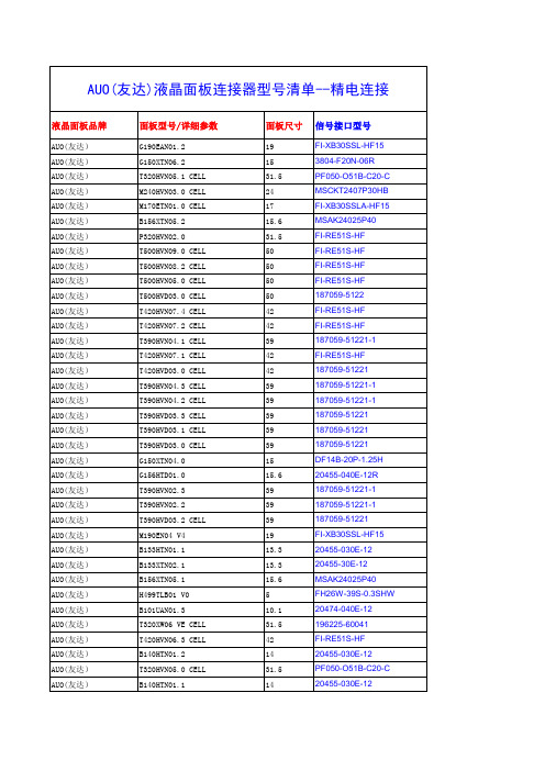
面板尺寸
19 15 31.5 24 17 15.6 31.5 50 50 50 50 42 42 39 42 42 39 39 39 39 39 15 15.6 39 39 39 19 13.3 13.3 15.6 5 10.1 31.5 42 14 31.5 14
信号接口型号
FI-XB30SSL-HF15 3804-F20N-06R PF050-O51B-C20-C MSCKT2407P30HB FI-XB30SSLA-HF15 MSAK24025P40 FI-RE51S-HF FI-RE51S-HF FI-RE51S-HF FI-RE51S-HF 187059-5122 FI-RE51S-HF FI-RE51S-HF 187059-51221-1 FI-RE51S-HF 187059-51221 187059-51221-1 187059-51221-1 187059-51221 187059-51221 187059-51221 DF14B-20P-1.25H 20455-040E-12R 187059-51221-1 187059-51221-1 187059-51221 FI-XB30SSL-HF15 20455-030E-12 20455-30E-12 MSAK24025P40 FH26W-39S-0.3SHW 20474-040E-12 196225-60041 FI-RE51S-HF 20455-030E-12 PF050-O51B-C20-C 20455-030E-12
AUO(友达) AUO(友达) AUO(友达) AUO(友达) AUO(友达) AUO(友达) AUO(友达) AUO(友达) AUO(友达) AUO(友达) AUO(友达) AUO(友达) AUO(友达) AUO(友达) AUO(友达) AUO(友达) AUO(友达) AUO(友达) AUO(友达) AUO(友达) AUO(友达) AUO(友达) AUO(友达) AUO(友达) AUO(友达) AUO(友达) AUO(友达) AUO(友达) AUO(友达) AUO(友达) AUO(友达) AUO(友达) AUO(友达) AUO(友达) AUO(友达) AUO(友达) AUO(友达) AUO(友达) AUO(友达) AUO(友达) AUO(友达) AUO(友达)
AS-PS02 AS-PS02A 安裝說明说明书
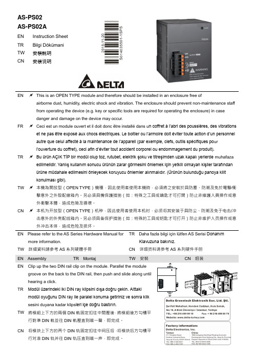
AS-PS02AS-PS02AEN Instruction SheetTR Bilgi DökümaniTW安裝說明CN安装说明EN This is an OPEN TYPE module and therefore should be installed in an enclosure free of airborne dust, humidity, electric shock and vibration. The enclosure should prevent non-maintenance staff from operating the device (e.g. key or specific tools are required for operating the enclosure) in casedanger and damage on the device may occur.FR Ceci est un module ouvert et il doit donc être installé dans u n coffret à l’abri des poussières, des vibrations et ne pas être exposé aux chocs électriques. Le boitier ou l’armoire doit éviter toute action d’un personnel autre que celui affecté à la maintenance de l’appareil (par exemple, clefs, outils spécifiques po url’ouverture du coffret), ceci afin d’éviter tout accident corporel ou endommagement du produit).TR Bu ürün AÇIK TİP bir modül olup toz, rutubet, elektrik şoku ve titreşimden uzak kapalı yerlerde muhafaza edilmelidir. Yanlış kullanım sonucu ürünün zarar görmesini önlemek için yetkili olmayan kişiler tarafındanürüne müdahale edilmesini önleyecek koruyucu önlemler alınmalıdır. (Ürünün bulunduğu panoya kilitkonulması gibi).TW 本機為開放型(OPEN TYPE)機種,因此使用者使用本機時,必須將之安裝於具防塵、防潮及免於電擊∕衝擊意外之外殼配線箱內。
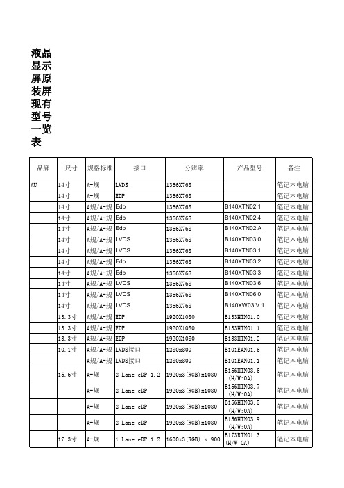
2015-04笔记本电脑显示屏现有型号一览表
LVDS接口 LVDS接口 EDP接口
HB140FH1-301镜面 笔记本电脑 HB140FH1-401雾01 HB133WX1-402 IT1160030 笔记本电脑 笔记本电脑 笔记本电脑 笔记本电脑
LED驱动/EDP接口 1366X768 LED驱动/EDP接口 1366X768 EDP接口 1366X768
A规/A-规 Edp A规/A-规 Edp A规/A-规 Edp A规/A-规 LVDS A规/A-规 LVDS A规/A-规 Edp A规/A-规 Edp A规/A-规 LVDS A规/A-规 LVDS A规/A-规 LVDS A规/A-规 EDP A规/A-规 EDP A规/A-规 EDP A规/A-规 LVDS接口 A规/A-规 LVDS接口
液晶显示屏原装屏现有型号一览表
品牌 AU 尺寸 14寸 14寸 14寸 14寸 14寸 14寸 14寸 14寸 14寸 14寸 14寸 14寸 13.3寸 13.3寸 13.3寸 10.1寸 规格标准 A-规 A-规 LVDS EDP 接口 分辨率 1366X768 1366X768 1366X768 1366X768 1366X768 1366X768 1366X768 1366X768 1366X768 1366X768 1366X768 1366X768 1920X1080 1920X1080 1920X1080 1280x800 1280x800
B4NT116WHM-N10 笔记本电脑 N140HGE-EAA AG 笔记本电脑 N140HGE-EBA Glare 笔记本电脑 1N116BGE-EA2 笔记本电脑 M185BGE-L23 一体机 M236HGE-L23 电视机 M236HGE-L20 电视机
B140XTN02.1 B140XTN02.4 B140XTN02.A B140XTN03.0 B140XTN03.1 B140XTN03.2 B140XTN03.3 B140XTN03.6 B140XTN06.0 B140XW03 V.1
Modicon ABLM1A24012电源供应设备说明书
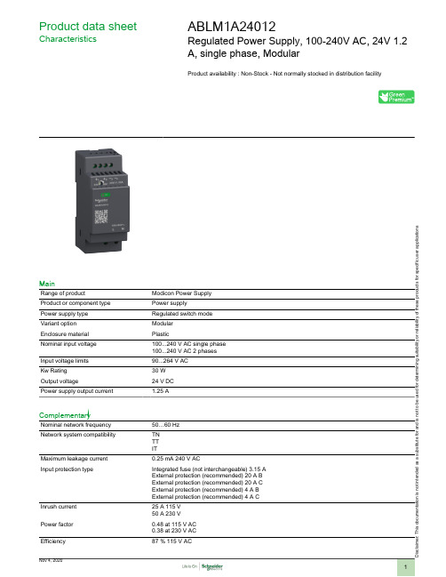
Product data sheetCharacteristicsABLM1A24012Regulated Power Supply, 100-240V AC, 24V 1.2A, single phase, ModularProduct availability : Non-Stock - Not normally stocked in distribution facilityMainRange of productModicon Power Supply Product or component type Power supplyPower supply type Regulated switch mode Variant option Modular Enclosure material PlasticNominal input voltage 100...240 V AC single phase 100...240 V AC 2 phases Input voltage limits 90...264 V AC Kw Rating 30 W Output voltage24 V DC Power supply output current1.25 AComplementaryNominal network frequency 50…60 Hz Network system compatibilityTN TT ITMaximum leakage current 0.25 mA 240 V ACInput protection typeIntegrated fuse (not interchangeable) 3.15 A External protection (recommended) 20 A B External protection (recommended) 20 A C External protection (recommended) 4 A B External protection (recommended) 4 A C Inrush current 25 A 115 V 50 A 230 V Power factor 0.48 at 115 V AC 0.38 at 230 V AC Efficiency87 % 115 V ACi s c l a i m e r : T h i s d o c u m e n t a t i o n i s n o t i n t e n d e d a s a s u b s t i t u t e f o r a n d i s n o t t o b e u s e d f o r d e t e r m i n i n g s u i t a b i l i t y o r r e l i a b i l i t y o f t h e s e p r o d u c t s f o r s p e c i f i c u s e r a p p l i c a t i o n s87 % 230 V ACOutput voltage adjustment24...28 VPower dissipation in W5 WCurrent consumption< 0.8 A 115 V AC< 0.6 A 230 V ACTurn-on time< 2 sHolding time> 20 ms 115 V AC> 60 ms 230 V ACStartup with capacitive loads3000 µFResidual ripple< 100 mVExpected capacitor life time10 year(s)Meantime between failure [MTBF]2500000 h at 77 °F (25 °C), full load1000000 h at 131 °F (55 °C), 80 % loadOutput protection type Against overload and short-circuits automatic resetAgainst over temperature manual resetAgainst overvoltage manual resetConnections - terminals Screw connection 0.5...1.5 mm², AWG 20...AWG 16) without wire end ferrule input/outputScrew connection 0.5...1 mm², AWG 20...AWG 18) with wire end ferrule input/output Line and load regulation< 0.5 %line< 1 %loadStatus LED Output voltage 1 LED Green)Maximum Depth 2.19 in (55.6 mm)Maximum Height 3.58 in (91 mm)Maximum Width 1.42 in (36 mm)Net Weight0.37 lb(US) (0.170 kg)Output coupling SerialParallelMounting support Top hat type TH35-15 rail IEC 60715Top hat type TH35-7.5 rail IEC 60715Double-profile DIN railpanel mountingEnvironmentStandards EN 62368-1EN/IEC 61010-1EN 61010-2-201EN/IEC 61204-3EN 61000-6-1EN 61000-6-2EN 61000-6-3EN 61000-6-4EN 61000-3-2EN 61000-3-3UL 62368-1UL 61010-1UL 61010-2-201CSA C22.2 No 62368-1CSA C22.2 No 61010-1CSA C22.2 No 61010-2-201Product certifications CECUL ListedCUL RecognizedRCMCB SchemeEACKCNEC class 2Operating altitude< 6561.68 ft (2000 m) overvoltage category III2000 m...5000 m overvoltage category IIShock resistance100 m/s² 11 msIP degree of protection IP20Ambient air temperature for operation-13…131 °F (-25…55 °C) without current derating)131…158 °F (55…70 °C) with current derating of 2.67 % per °C)Ambient air temperature for storage-40…185 °F (-40…85 °C)Relative humidity0…95 % without condensationOvervoltage category IIElectrical shock protection class Class II without PE connectionPollution degree2Vibration resistance 3 mm 2…9 Hz)IEC 60721-3-310 m/s² 9…200 Hz)IEC 60721-3-3Electromagnetic immunity Immunity to electrostatic discharge 6 kV contact discharge) EN/IEC 61000-4-2Immunity to electrostatic discharge 9 kV air discharge) EN/IEC 61000-4-2Electromagnetic field immunity test 10 V/m 80 MHz...2 GHz) EN/IEC 61000-4-3Electromagnetic field immunity test 5 V/m 2...2.7 GHz) EN/IEC 61000-4-3Electromagnetic field immunity test 3 V/m 2.7...6 GHz) EN/IEC 61000-4-3Immunity to fast transients 4 kV on input-output) EN/IEC 61000-4-4Surge immunity test 3 kV between power supply and earth) EN/IEC 61000-4-5Surge immunity test 1.5 kV between phases) EN/IEC 61000-4-5Immunity to conducted disturbances 10 Vrms 0.15...80 MHz) EN/IEC 61000-4-6Immunity to magnetic fields 30 A/m 50...60 Hz) EN/IEC 61000-4-8Immunity to voltage dips 100 % 1 cycle) EN/IEC 61000-4-11Immunity to voltage dips 60 % 10 cycles) EN/IEC 61000-4-11Immunity to voltage dips 30 % 25 cycles) EN/IEC 61000-4-11Disturbing field emission EN 55016-2-3Limits for harmonic current emissions EN 61000-3-2Conducted disturbance emission EN 55016-1-2Conducted disturbance emission EN 55016-2-1Electromagnetic emission Conducted emissions EN 61000-6-3Radiated emissions EN 61000-6-4Dielectric strength3000 V AC input/outputOrdering and shipping detailsCategory22525 - ABL8 AND ABL7 POWER SUPPLIEDiscount Schedule CP12GTIN00785901704706Package weight(Lbs)1 lb(US) (0.45 kg)Returnability YesCountry of origin CNOffer SustainabilitySustainable offer status Green Premium productREACh Regulation REACh DeclarationEU RoHS Directive Pro-active compliance (Product out of EU RoHS legal scope)EU RoHS DeclarationMercury free YesRoHS exemption information YesChina RoHS Regulation China RoHS declarationEnvironmental Disclosure Product Environmental ProfileCircularity Profile End of Life InformationWEEE The product must be disposed on European Union markets following specific waste collection andnever end up in rubbish bins.Electrical Safety●If the unit is use in a manner not specified by the manufacturer, the protection provided by the equipment may be impaired.●For means of disconnection a switch or circuit breaker, located near the product, must be included in the installation. A marking as disconnecting device for th ●The device has an internal fuse. The unit is tested and approved with branch circuit protective device up to 20A. This circuit breaker can be used as disconne ●The power supply is only suitable for audio, video, information, communication, industrial and control equipment.DimensionsSide and Rear ViewConnections and SchemaConnections and Schema Correct Parallel Connection(1) :LoadIncorrect Parallel Connection(1) :LoadABLx1Axxxxx-1 = ABLx1Axxxxx-2 max 2 x ABLx1AxxxxxL1 = L2∆V max 25 mVL Load < 90% 2 x L nomOutput Voltage Balancing(1) :R Load1(2) :R Load2R Load1= R Load2I1= I 2= ~ I nomSeries Connection(1) :V out1(2) :V out2(3) : 2 x Diode, V RRM> 2 x V out1/2, I F > 2 x I nom1/2(4) :V Load = 2 x V out(5) :LoadConnections and Schema Connections and Schema(1) :AmbientPerformance Curves Performance CurveX :Ambient Temperature (ºC)Y :Percentage of Max Load (%)1 :Mounting A & B, altitude 2000M2 :Mounting A & B, altitude 5000MMounting and ClearanceMountingMounting Position AMounting Position BIncorrect Mounting。
ABB低压继电器手册
2CDC 293 034 F0004
ᕃ ᕄ ᕆ ᕅ ᕇ
1 c/o contact: 250 V, 16 A CR-P012DC1 CR-P024DC1 CR-P048DC1 CR-P110DC1 CR-P024AC1 CR-P048AC1 CR-P110AC1 CR-P120AC1 CR-P230AC1 CR-P012DC2 CR-P024DC2 CR-P048DC2 CR-P110DC2 CR-P024AC2 CR-P048AC2 CR-P110AC2 CR-P120AC2 CR-P230AC2 12 V DC 24 V DC 48 V DC 110 V DC 24 V AC 48 V AC 110 V AC 120 V AC 230 V AC 12 V DC 24 V DC 48 V DC 110 V DC 24 V AC 48 V AC 110 V AC 120 V AC 230 V AC 1SVR 405 600 R4000 1SVR 405 600 R1000 1SVR 405 600 R6000 1SVR 405 600 R8000 1SVR 405 600 R0000 1SVR 405 600 R5000 1SVR 405 600 R7000 1SVR 405 600 R2000 1SVR 405 600 R3000 1SVR 405 601 R4000 1SVR 405 601 R1000 1SVR 405 601 R6000 1SVR 405 601 R8000 1SVR 405 601 R0000 1SVR 405 601 R5000 1SVR 405 601 R7000 1SVR 405 601 R2000 1SVR 405 601 R3000 10 10 10 10 10 10 10 10 10 10 10 10 10 10 10 10 10 10
B101AW06 Functional Spec V1-LED_O_0A_032910

( V ) Preliminary Specifications ( ) Final SpecificationsModule 10.1”(10.06”) SD 16:9 Color TFT-LCD with LED Backlight design Model Name B101AW06 V1 (H/W:0A)Note ()LED Backlight with driving circuit designCustomerDateChecked & Approved byDateNote: This Specification is subject to change without notice.Approved by DateCH Lin03/29/2010Prepared by DateMarcus Yen03/29/2010NBBU Marketing Division AU Optronics corporationContents1. Handling Precautions (4)2. General Description (5)2.1 General Specification (5)2.2 Optical Characteristics (6)3. Functional Block Diagram (11)4. Absolute Maximum Ratings (12)4.1 Absolute Ratings of TFT LCD Module (12)4.2 Absolute Ratings of Environment (12)5. Electrical Characteristics (13)5.1 TFT LCD Module (13)5.2 Backlight Unit (15)6. Signal Interface Characteristic (16)6.1 Pixel Format Image (16)6.2 The Input Data Format (17)6.3 Integration Interface Requirement (18)6.4 Interface Timing (20)7. Panel Reliability Test (22)7.1 Vibration Test (22)7.2 Shock Test (22)7.3 Reliability Test (22)8. Mechanical Characteristics (23)8.1 LCM Outline Dimension (23)9. Shipping and Package (25)9.1 Shipping Label Format (25)9.2 Carton Package (26)9.3 Shipping Package of Palletizing Sequence (26)10. Appendix: EDID Description (27)Record of RevisionVersion and Date Page Old description New Description Remark 0.1 2009/12/02 All First Edition for Customer0.2 2009/12/14 15 PWM Input Frequency100(Min),200(Typ),20K(Max) Follow Customer Request 700(Min),1K(Typ),2K(Max)0.3 2009/12/23 18 Update Pin Assignment0.4 2010/01/10 24 Update Module drawing0.5 2010/02/22 14 Update 5.1.2, EDID0.6 2010/03/10 25 Update Label0.7 2010/03/29 15,20 Update PWM duty and ClockFrequency typ.1. Handling Precautions1) Since front polarizer is easily damaged, pay attention not to scratch it.2) Be sure to turn off power supply when inserting or disconnecting from inputconnector.3) Wipe off water drop immediately. Long contact with water may cause discolorationor spots.4) When the panel surface is soiled, wipe it with absorbent cotton or other soft cloth.5) Since the panel is made of glass, it may break or crack if dropped or bumped onhard surface.6) Since CMOS LSI is used in this module, take care of static electricity and insurehuman earth when handling.7) Do not open nor modify the Module Assembly.8) Do not press the reflector sheet at the back of the module to any directions.9) At the insertion or removal of the Signal Interface Connector, be sure not to rotatenor tilt the Interface Connector of the TFT Module.11)After installation of the TFT Module into an enclosure (Notebook PC Bezel, forexample), do not twist nor bend the TFT Module even momentary. At designing the enclosure, it should be taken into consideration that no bending/twisting forces are applied to the TFT Module from outside. Otherwise the TFT Module may be damaged.12) S mall amount of materials having no flammability grade is used in the LCD module. TheLCD module should be supplied by power complied with requirements of Limited Power Source (IEC60950 or UL1950), or be applied exemption.13) D isconnecting power supply before handling LCD modules, it can prevent electric shock,DO NOT TOUCH the electrode parts, cables, connectors and LED circuit part of TFT module that a LED light bar build in as a light source of back light unit. It can prevent electrostic breakdown.2. General DescriptionB101AW06 V1 is a Color Active Matrix Liquid Crystal Display composed of a TFT LCD panel, a driver circuit, and LED backlight system. The screen format is intended to support the 16:9 SD, 1024(H) x600(V) screen and 262k colors (RGB 6-bits data driver) with LED backlight driving circuit. All input signals are LVDS interface compatible.B101AW06 V1 is designed for a display unit of notebook style personal computer and industrial machine.2.1 General SpecificationThe following items are characteristics summary on the table at 25 ℃ condition:ItemsUnit SpecificationsScreen Diagonal [mm] 255.537Active Area [mm] 222.72 (H) X125.28 (V) Pixels H x V 1024x 600x 3(RGB) Pixel Pitch [mm] 0.2175 (H)X0.2088 (V) Pixel Format R.G.B. Horizontal Stripe Display ModeNormally WhiteWhite Luminance (I LED =20mA)(Note: ILED is LED current)[cd/m 2] 200 typ. (5 points average)170 min. (5 points average) Luminance Uniformity 1.25 max. (5 points) Contrast Ratio 400 typ Response Time[ms] 16 typ / 25 Max Nominal Input Voltage VDD [Volt] +3.3 typ.Power Consumption [Watt]2.6 max. (Include Logic and Blu power)Weight[Grams] 170 max. Min.Typ.Max. Length 244.5 245.0 245.5 Width 146.0 146.5 147.0 Physical Size Include bracket [mm] Thickness - -3.6Electrical Interface 1 channel LVDS Glass Thickness [mm] 0.5Surface Treatment Glare, Hardness 3H,Reflection 4.3%Support Color262K colors ( RGB 6-bit )Temperature Range OperatingStorage (Non-Operating) [oC] [oC]0 to +50 -20 to +60RoHS ComplianceRoHS Compliance2.2 Optical CharacteristicsThe optical characteristics are measured under stable conditions at 25℃ (Room Temperature) :ItemSymbolConditions Min. Typ. Max. Unit Note White LuminanceI LED =20mA5 points average170 200 - cd/m 21, 4, 5.θR θL Horizontal (Right) CR = 10 (Left) 40 40 45 45 - - degreeViewing AngleψH ψL Vertical (Upper) CR = 10 (Lower)10 30 15 35 - -4, 9Luminance Uniformity δ5P 5 Points - - 1.25 1, 3, 4 Luminance Uniformity δ13P 13 Points- - 1.60 2, 3, 4 Contrast Ratio CR 300 400 - 4, 6 Cross talk % 44, 7T r Rising - 9 - T f Falling - 7 - Response TimeT RTRising + Falling-1625msec 4, 8Rx 0.562 0.592 0.622 RedRy 0.316 0.346 0.376 Gx 0.299 0.329 0.359 GreenGy 0.512 0.542 0.572Bx 0.119 0.149 0.179 BlueBy 0.115 0.145 0.175 Wx 0.263 0.313 0.363 Color / ChromaticityCoodinates WhiteWy 0.279 0.329 0.379 NTSC%CIE 1931-45-4Note 1: 5 points position (Ref: Active area)Note 2: 13 points position (Ref: Active area)Note 3: The luminance uniformity of 5 or13 points is defined by dividing the maximum luminance values by the minimum test point luminanceNote 4: Measurement methodThe LCD module should be stabilized at given temperature for 30 minutes to avoid abrupt temperature change during measuring. In order to stabilize the luminance, the measurement should be executed afterδW13 = Maximum Brightness of thirteen pointsMinimum Brightness of thirteen pointsMaximum Brightness of five pointsδW5 = Minimum Brightness of five pointslighting Backlight for 30 minutes in a stable, windless and dark room, and it should be measured in the center of screen.Note 5: Definition of Average Luminance of White (Y L ):Measure the luminance of gray level 63 at 5 points ,Y L = [L (1)+ L (2)+ L (3)+ L (4)+ L (5)] / 5 L (x) is corresponding to the luminance of the point X at Figure in Note (1).Note 6: Definition of contrast ratio:Contrast ratio is calculated with the following formula.Note 7: Definition of Cross Talk (CT)CT = | Y B – Y A | / Y A × 100 (%) WhereY A = Luminance of measured location without gray level 0 pattern (cd/m 2) Y B = Luminance of measured location with gray level 0 pattern (cd/m 2)Contrast ratio (CR)=Brightness on the “White” state Brightness on the “Black” stateNote 8: Definition of response time:The output signals of BM-7 or equivalent are measured when the input signals are changed from “Black” to “White” (falling time) and from “White” to “Black” (rising time), respectively. The response time interval between the 10% and 90% of amplitudes. Refer to figure as below.Note 9. Definition of viewing angleViewing angle is the measurement of contrast ratio ≧10, at the screen center, over a 180° horizontal an d 180° vertical range (off-normal viewing angles). Th e 180° viewing angle range is broken down as follow s; 90°(θ) horizontal left and right and 90° (Φ) vertical, high (up) and low (down). The measurement direction is typically perpendicular to the display surface with the screen rotated about its center to develop the desired measurement viewing angle.3. Functional Block DiagramThe following diagram shows the functional block of the 10.1 inches wide Color TFT/LCD 40 Pin one channel Module4. Absolute Maximum RatingsAn absolute maximum rating of the module is as following:4.1 Absolute Ratings of TFT LCD ModuleItem Symbol Min Max Unit Conditions Logic/LCD Drive Vin -0.3 +4.0 [Volt] Note 1,25. Electrical Characteristics 5.1 TFT LCD Module5.1.1 Power SpecificationInput power specifications are as follows;The power specification are measured under 25℃ and frame frenquency under 60HzSymble Parameter Min Typ Max UnitsNote VDD Logic/LCD Drive Voltage 3.0 3.3 3.6 [Volt] PDD VDD Power - 0.8 - [Watt] Note 1 IDD IDD Current -240- [mA] Note 1 I Rush Inrush Current - - 2000 [mA] Note 2VDDrpAllowableLogic/LCD Drive Ripple Voltage--100[mV] p-pNote 1 : Maximum Measurement Condition :Black Pattern at 3.3V driving voltage. (P max =V 3.3 x I black ) Note 2:Measure ConditionVin rising time0V3.3V5.1.2 Signal Electrical CharacteristicsInput signals shall be low or High-impedance state when VDD is off.Signal electrical characteristics are as follows;Parameter Condition Min Max UnitV TH Differential Input HighThreshold (Vcm=+1.2V) 100[mV]V TL Differential Input LowThreshold (Vcm=+1.2V) -100 -[mV]|V ID| Differential InputVoltage 100 600 [mV]V CM Differential InputCommon Mode VoltagelVIDl / 2 2.4 - lVIDl / 2 [V] Note: LVDS Signal Waveform15 of 29AU OPTRONICS CORPORATIONProduct SpecificationB101AW06 V0 Document Version : 0.7 5.2 Backlight Unit5.2.1 LED characteristicsParameter Symbol Min Typ Max Units ConditionBacklight Power Consumption PLED - 1.506 1.647 [Watt] (Ta=25℃), Note 1Vin =12V LED Life-TimeN/A10,000--Hour (Ta=25℃), Note 2I F =20 mANote 1: Calculator value for reference P LED = V F (Normal Distribution) * I F (Normal Distribution) / Efficiency Note 2: The LED life-time define as the estimated time to 50% degradation of initial luminous.5.2.2 Backlight input signal characteristicsParameterSymbol Min Typ Max Units RemarkLED Power Supply VLED 5.0 12.0 21.0 [Volt] LED Enable Input High Level 2.5 - 5.5 [Volt] LED Enable Input Low LevelVLED_EN- - 0.8 [Volt] PWM Logic Input High Level 2.5 - 5.5 [Volt] PWM Logic Input Low LevelVPWM_EN-- 0.8 [Volt] PWM Input Frequency FPWM 100 200 20K Hz PWM Duty RatioDuty5--100%Define as Connector Interface (Ta=25℃)6. Signal Interface Characteristic 6.1 Pixel Format ImageFollowing figure shows the relationship of the input signals and LCD pixel format.1 1024 1st Line600th Line6.2 The Input Data FormatSignal Name DescriptionR5 R4 R3 R2 R1 R0 Red Data 5 (MSB)Red Data 4Red Data 3Red Data 2Red Data 1Red Data 0 (LSB)Red-pixel DataRed-pixel DataEach red pixel's brightness data consists ofthese 6 bits pixel data.G5 G4 G3 G2 G1 G0 Green Data 5 (MSB)Green Data 4Green Data 3Green Data 2Green Data 1Green Data 0 (LSB)Green-pixel DataGreen-pixel DataEach green pixel's brightness data consists ofthese 6 bits pixel data.B5 B4 B3 B2 B1 B0 Blue Data 5 (MSB)Blue Data 4Blue Data 3Blue Data 2Blue Data 1Blue Data 0 (LSB)Blue-pixel DataBlue-pixel DataEach blue pixel's brightness data consists ofthese 6 bits pixel data.RxCLKIN Data Clock The signal is used to strobe the pixel data andDE signals. All pixel data shall be valid at thefalling edge when the DE signal is high.DE Display Timing This signal is strobed at the falling edge ofRxCLKIN. When the signal is high, the pixeldata shall be valid to be displayed.VS Vertical Sync The signal is synchronized to RxCLKIN .HS Horizontal Sync The signal is synchronized to RxCLKIN . Note: Output signals from any system shall be low or High-impedance state when VDD is off.6.3 Integration Interface Requirement6.3.1 Connector DescriptionPhysical interface is described as for the connector on module.These connectors are capable of accommodating the following signals and will be following components.Connector Name / Designation For Signal ConnectorManufacturer IPEX or compatibleType / Part Number IPEX 20455-040E-12R or compatibleMating Housing/Part Number IPEX 20453-040T-116.3.2 Pin AssignmentLVDS is a differential signal technology for LCD interface and high speed data transfer device.PIN# Signal Name Description1NC No connect2VDD Power Supply +3.3V3VDD Power Supply +3.3V4VEDID EDID +3.3V Power5NC No Connect6CLK_EDID EDID Clock Input7DATA_EDID EDID Data Input8RxOIN0--LVDS Differential Data (Odd R0-R5, G0)9RxOIN0++LVDS Differential Data (Odd R0-R5, G0)10VSS Ground11RxOIN1--LVDS Differential Data (Odd G1-G5,B0-B1)12RxOIN1++LVDS Differential Data (Odd G1-G5,B0-B1)13VSS Ground14RxOIN2--LVDS Differential Data (Odd B2-B5,HS,VS,DE)15RxOIN2++LVDS Differential Data (Odd B2-B5,HS,VS,DE)16VSS Ground17RxOCKIN--LVDS Odd Differential CLK18RxOCKIN++LVDS Odd Differential CLK19VSS Ground20NC No Connect21NC No ConnectNote1: Input signals shall be low or High-impedance state when VDD is off.Pin 40 VLEDNCPin 16.4 Interface Timing6.4.1 Timing CharacteristicsBasically, interface timings should match the 1024x600 /60Hz manufacturing guide line timing.Parameter SymbolMin. Typ. Max. Unit Frame Rate - - - - Hz Clock frequency 1/ T Clock 20 49.8 75 MHzPeriod T V 614-1024Active T VD600 Vertical SectionBlanking T VB 14 - 424 T Line Period T H 1064 -2048Active T HD 1024 Horizontal SectionBlankingT HBh-128 h (Note1)h+128 T ClockNote : DE mode onlyNote1 : H-Blanking support +/- 128 LVDS clock variation6.4.2 Timing diagramDOTCLKDEHDET VDInput Timing Definition ( DE Mode)Input Data Invaild Data Invaild Data6.5 Power ON/OFF SequencePower on/off sequence is as follows. Interface signals and LED on/off sequence are also shown inthe chart. Signals from any system shall be Hi-Z state or low level when VDD is offPower Sequence TimingValueParameter Min. Max. UnitsT1 0.510T2 050T3 200-T4 200-T5 050T6 010msT7 500-T8 10-T9 10180T10 10180T11 10-T12 0.5107. Panel Reliability Test7.1 Vibration TestTest Spec:Test method: Non-OperationAcceleration: 1.5 GFrequency: 10 - 500Hz RandomSweep: 30 Minutes each Axis (X, Y, Z)7.2 Shock TestTest Spec:Test method: Non-OperationAcceleration: 220 G , Half sine waveActive time: 2 msPulse: X,Y,Z .one time for each side7.3 Reliability TestItems Required Condition Note TemperatureHumidity BiasTa= 40℃, 90%RH, 300hHigh TemperatureOperationTa= 50℃, Dry, 300hLow TemperatureOperationTa= 0℃, 300hHigh TemperatureStorageTa= 60℃, 35%RH, 300hLow TemperatureStorageTa= -20℃, 50%RH, 250hThermal ShockTestTa=-20℃to 60℃, Duration at 30 min, 100 cyclesESD Contact : ±8 KVAir : ±15 KVNote 1Note1: According to EN 61000-4-2 , ESD class B: Some performance degradation allowed. Self-recoverable.No data lost, No hardware failures.Remark: MTBF (Excluding the LED): 30,000 hours with a confidence level 90%23 of 298. Mechanical Characteristics 8.1 LCM Outline Dimension24 of 29B101AW06 V0 Document Version : 0.78.1.2 Standard Rear View9. Shipping and Package9.1 Shipping Label FormatH/W9.2 Carton Package9.3 Shipping Package of Palletizing Sequence10. Appendix: EDID DescriptionAddress FUNCTION Value Value Value Note HEX HEX BIN DEC00 Header 00 00000000 001 FF 11111111 25502 FF 11111111 25503 FF 11111111 25504 FF 11111111 25505 FF 11111111 25506 FF 11111111 25507 00 00000000 008 EISA Manuf. Code LSB 06 00000110 609 Compressed ASCII AF 10101111 1750A Product Code D2 11010010 2100B hex, LSB first 61 01100001 970C 32-bit ser # 00 00000000 00D 00 00000000 00E 00 00000000 00F 00 00000000 010 Week of manufacture 00 00000000 011 Year of manufacture 13 00010011 1912 EDID Structure Ver. 01 00000001 113 EDID revision # 03 00000011 314 Video input def. (digital I/P, non-TMDS, CRGB)80 10000000 12815 Max H image size (rounded to cm)16 00010110 2216 Max V image size (rounded to cm)0D 00001101 1317 Display Gamma (=(gamma*100)-100)78 01111000 12018 Feature support (no DPMS, Active OFF, RGB, tmg Blk#1)0A 00001010 1019 Red/green low bits (Lower 2:2:2:2 bits)15 00010101 211A Blue/white low bits (Lower 2:2:2:2 bits)85 10000101 1331B Red x (Upper 8 bits)97 10010111 1511C Red y/ highER 8 bits 58 01011000 881D Green x 53 01010011 831E Green y 8A 10001010 1381F Blue x 26 00100110 3820 Blue y 25 00100101 3721 White x 50 01010000 8022 White y 54 01010100 8423 Established timing 1 00 00000000 024 Established timing 2 00 00000000 025 Established timing 3 00 00000000 026 Standard timing #1 01 00000001 127 01 00000001 128 Standard timing #2 01 00000001 129 01 00000001 12A Standard timing #3 01 00000001 12B 01 00000001 1 2C Standard timing #4 01 00000001 1 2D 01 00000001 1 2E Standard timing #5 01 00000001 1 2F 01 00000001 130 Standard timing #6 01 00000001 131 01 00000001 132 Standard timing #7 01 00000001 133 01 00000001 134 Standard timing #8 01 00000001 135 01 00000001 136 Pixel Clock/10000 LSB 74 01110100 11637 Pixel Clock/10000 USB 13 00010011 1938 Horz active Lower 8bits00 00000000 039 Horz blanking Lower 8bits3A 00111010 58 3A HorzAct:HorzBlnk Upper 4:4 bits41 01000001 65 3B Vertical Active Lower 8bits58 01011000 88 3C Vertical Blanking Lower 8bits14 00010100 20 3D Vert Act : Vertical Blanking (upper 4:4 bit)20 00100000 32 3E HorzSync. Offset 30 00110000 48 3F HorzSync.Width 20 00100000 3240 VertSync.Offset : VertSync.Width 26 00100110 3841 Horz&Vert Sync Offset/Width Upper 2bits00 00000000 042 Horizontal Image Size Lower 8bits DE 11011110 22243 Vertical Image Size Lower 8bits7D 01111101 12544 Horizontal & Vertical Image Size (upper 4:4 bits)00 00000000 045 Horizontal Border (zero for internal LCD)00 00000000 046 Vertical Border (zero for internal LCD)00 00000000 047 Signal (non-intr, norm, no stero, sep sync, neg pol)18 00011000 2448 Detailed timing/monitor 00 00000000 049 descriptor #2 00 00000000 0 4A 00 00000000 0 4B 0F 00001111 15 4C 00 00000000 0 4D 00 00000000 0 4E 00 00000000 0 4F 00 00000000 050 00 00000000 051 00 00000000 052 00 00000000 053 00 00000000 054 00 00000000 055 00 00000000 056 00 00000000 057 00 00000000 058 00 00000000 05A Detailed timing/monitor 00 00000000 05B descriptor #3 00 00000000 05C 00 00000000 05D FE 11111110 2545E 00 00000000 05F Manufacture 41 01000001 65 A60 Manufacture 55 01010101 85 U61 Manufacture 4F 01001111 79 O62 0A 00001010 1063 20 00100000 3264 20 00100000 3265 20 00100000 3266 20 00100000 3267 20 00100000 3268 20 00100000 3269 20 00100000 326A 20 00100000 326B 20 00100000 326C Detailed timing/monitor 00 00000000 06D descriptor #4 00 00000000 06E 00 00000000 06F FE 11111110 25470 00 00000000 071 Manufacture P/N 42 01000010 66 B72 Manufacture P/N 31 00110001 49 173 Manufacture P/N 30 00110000 48 074 Manufacture P/N 31 00110001 49 175 Manufacture P/N 41 01000001 65 A76 Manufacture P/N 57 01010111 87 W77 Manufacture P/N 30 00110000 48 078 Manufacture P/N 36 00110110 54 679 Manufacture P/N 20 00100000 327A Manufacture P/N 56 01010110 86 V 7B Manufacture P/N 31 00110001 49 1 7C 20 00100000 327D 0A 00001010 107E Extension Flag 00 00000000 07F Checksum 29 00101001 41。
西门子技术问题总汇

文档标题
如何设置模拟量输入模板 SM 431-7KF00的温度补偿? 如何解决 SIMATIC BATCH 的 IL43基本设备上 hotfix 安装的问题? 如果通过 PCS7 V6.1 SP1 DVD 单独安装 SIMATIC BATCH Report 需要注意哪些设置? 为什么冗余模拟量输出模块的每个通道只有一半电流输出? 使用WinCC/Web Navigator V6.1 SP1需要什么样的操作系统和软件? 是否 COM PROFIBUS 可以使用所有版本的 GSD 文件? 如何在 WinCC flexible 中组态与S7 控制器的 Profinet 连接? 如何在操作面板上设定定时器时间, 同时如何输出定时器的剩余时间? 数据块初始值与实际值的含义 如何通过窗口对象滚动条步进调节过程值参数? 使用 SINAUT ST7 向电子邮箱接受方发送文本信息 SMS 需要做何设置? 可以使用CPU317-2PN/DP替代在iMap中组态的CPU315-2PN/DP吗? 什么情况下插入C-PLUG卡或者C-PLUG有什么作用? 通过一台PC,可以使用哪种方式访问与IWLAN/PB link PNIO或IE/PB link PNIO连接的PROFIBUS设备? 当在SINAUT网络中使用4线变压器应该注意哪些设置? 在 SINAUT 网络中,使用MD3拨号调制解调器作为专线调制解调器时,要进行哪些设置? 如何安装 DCF77 天线, 当选择 DCF77 天线时需要注意什么? 使用SINAUT ST7向传真机发送文本信息时,需要进行哪些设置? 在 SINAUT 项目中发送短消息必须进行哪些特殊服务的设置? 如何在S7-300 PN CPU和CP343-1之间建立一个open TCP 通讯连接,以及如何进行数据交换? 如何在两个S7-300 PN CPU之间建立一个open TCP 通讯连接,以及如何进行数据交换? 哪些控制系统可以成功与SINAUT ST7一起使用? 使用“零-Modem”电缆连接 TIM 模块应该注意什么? 当用 SINAUT 诊断工具的ST1协议进行诊断时,为什么TIM的状态不能显示? TIM 3V-IE 和 TIM 3V-IE Advanced 模块在以太网上通信时使用哪个端口号? 如何对没有接入网络的S7-200CPU编程? 掉电后,LOGO!的程序会丢失吗? 从 PCS7 V6.1 起,为什么没有分配任何 hierarchy (PH) 的 测量点(变量)通过编译不能在OS中自动创建相应的变量? 在SFC中,如何实现从一个 Sequencer 跳出后回到另一个 Sequencer 的某个固定位置并继续执行? 如何实现过程变量的平均值归档? 存储文件的目标路径和备份可选路径有何作用? WinCC变量归档中如何实现采集周期小于500ms的变量归档? 为什么在 OS 上会显示如下信息“时间跳变通知-永久切换为从站模式”? 在西门子A&D产品支持网站是否可以下载关于ET200M的手册? 在S7-400上怎样安装冗余电源? UDT改变后怎样更新使用UDT产生的数据块。 为什么在FB块中使用OUT变量赋值被调用FB块的IN变量时出现错误信息34:4469? 如何查看4-mation导入-导出错误 不能正确引导8212-1QU IBM/Lenovo M52 ThinkCentre 实时趋势更新缓慢的原因 如何保存变量名字典CSV文件的格式
- 1、下载文档前请自行甄别文档内容的完整性,平台不提供额外的编辑、内容补充、找答案等附加服务。
- 2、"仅部分预览"的文档,不可在线预览部分如存在完整性等问题,可反馈申请退款(可完整预览的文档不适用该条件!)。
- 3、如文档侵犯您的权益,请联系客服反馈,我们会尽快为您处理(人工客服工作时间:9:00-18:30)。
Product SpecificationAU OPTRONICS CORPORATION( v ) Preliminary Specifications ( ) Final Specifications Module Model Name Note 10.1” WXGA 16:10 Color TFT-LCD B101EAN02.0(91階, HW:1A) COG (open cell without PCBA)CustomerDateApproved byDateYW Lee01/16/2015Checked & Approved byDatePrepared by01/16/2015Note: This Specification is subject to change without notice.MPBU Marketing Division AU Optronics corporationB101EAN02.0Document Version : 0.11 of 32Product SpecificationAU OPTRONICS CORPORATIONContents1. Handling Precautions .............................................................. 4 2. General Description ................................................................ 52.1 General Specification ..........................................................................................................................5 2.2 Optical Characteristics ........................................................................................................................53. Electrical Characteristic ........................................................ 103.1 Power Specification...........................................................................................................................10 3.2 MIPI Command Specification...........................................................................................................12 3.3 Vcom Tuning Note ............................................................................................................................12 3.4 Vcom generate from PCBA PWMIC ................................................................................................13 3.5 Vcom generate from Single Chip ......................................................................................................14 3.6 power on/off sequence.......................................................................................................................14 3.7 Initial code.........................................................................................................................................15 3.8 Timing ...............................................................................................................................................154. Signal Interface Characteristic.............................................. 174.1 Pixel Format Image ...........................................................................................................................17 4.2 FPC Pin Assignment..........................................................................................................................18 4.3 FPC Side Bonding Pad Drawing .......................................................................................................245. Mechanical Characteristics.................................................... 255.1 Standard Front View..........................................................................................................................25 5.2 Standard Back View ..........................................................................................................................26 5.3 Rubbing 角度 ...................................................................................................................................27 5.4 Ag pad Position .................................................................................................................................296. Shipping and Package ........................................................... 306.1 Shipping Label Format ......................................................................................................................30 6.2 Carton Package..................................................................................................................................31 6.3 Shipping Package of Palletizing Sequence........................................................................................317. Panel Reliability Test ............................................................ 32B101EAN02.0Document Version : 0.12 of 32Product SpecificationAU OPTRONICS CORPORATIONRecord of RevisionVersion and Date 0.1 2015/01/16 Page All Old description First Edition for Customer New Description RemarkB101EAN02.0Document Version : 0.13 of 32Product SpecificationAU OPTRONICS CORPORATION1. Handling Precautions1) Since front polarizer is easily damaged, pay attention not to scratch it. 2) Wipe off water drop immediately. Long contact with water may cause discoloration or spots. 3) When the panel surface is soiled, wipe it with absorbent cotton or other soft cloth. 4) Since the panel is made of glass, it may break or crack if dropped or bumped on hard surface. 5) Since CMOS LSI is used in this module, take care of static electricity and insure human earth when handling.B101EAN02.0Document Version : 0.14 of 32Product SpecificationAU OPTRONICS CORPORATION2. General DescriptionB101EAN02.0 is a Color Active Matrix Liquid Crystal Display composed of a TFT LCD panel and a driver IC. The screen format is intended to support the 16:10 , 800(H) x1280(V) screen and 16.7M colors (RGB 8-bits data driver). All input signals are MIPI interface compatible. Panel chip IC support CABC (Content Adaptive Brightness Control), (IE) Image Enhancement and (SRE) Sunlight Readability Enhancement.2.1 General SpecificationThe following items are characteristics summary on the table at 25℃ condition:SpecificationsItems Screen Diagonal Active Area Pixels H x V Pixel Pitch Pixel Format Display Mode Response Time Nominal Input Voltage Weight Electrical Interface Glass Thickness Panel Thickness (max) Surface Treatment( panel only) Support Color IC model Temperature Range Operating Storage (Non-Operating) RoHS ComplianceUnit [mm] [mm] 255.397135.36(H) x 216.576(V) 800 x 3(RBG) x 1280[mm]0.1695 X 0.1695 R.G.B. Vertical Stripe AHVA, Normally Black[ms] [Volt] [Grams]30 typ / 35 Max Vin=3.3V typ. / VDDI=1.8V typ. 65max. MIPI[mm] [mm]0.25/0.25 0.84 max. HC RGB 8-bit OTM1287A[oC] [oC]0 to +50 -20 to +60 RoHS Compliance2.2 Optical CharacteristicsB101EAN02.0 Document Version : 0.15 of 32Product SpecificationAU OPTRONICS CORPORATION The optical characteristics are measured under stable conditions at 25 Item Symbol θR θL Viewing Angle ψH ψL Contrast Ratio Cross talk Response Time Red CR % TRT Rx Ry Green Gx Gy CIE 1931 Bx Blue By Wx White Wy % 0.269 0.305 Rising + Falling Vertical CR = 10 (Upper) (Lower) Conditions Horizontal CR = 10 (Right) (Left)℃ (Room Temperature) :Typ. 85 85 85 85 800 --30 TBD TBD TBD TBD TBD TBD 0.299 0.335 58 0.329 0.365 Pol: With Backlight (customer provide spectrum) (C-light Max. 4 35msec 1, 3 1, 4 5 Unit degree 1, 6 NoteMin. 600 ---Color / Chromaticity Coodinates源)光NTSC亮面Transmittance%5.46NABLU: C lightB101EAN02.0Document Version : 0.16 of 32Product SpecificationAU OPTRONICS CORPORATION Note 1: Measurement methodThe LCD module should be stabilized at given temperature for 30 minutes to avoid abrupt temperature change during measuring. In order to stabilize the luminance, the measurement should be executed after lighting Backlight for 30 minutes in a stable, windless and dark room, and it should be measured in the center of screen.Photo detectorField=2°50 cmLCD PanelTFT-LCD ModuleNote 2:Center of the screen Definition of Average Luminance of White (YL):Measure the luminance of gray level 63 at 5 points,Y = [L (1)+ L (2)+ L (3)+ L (4)+ L (5)] / 5LL (x) is corresponding to the luminance of the point X at Figure in Note (1).Note 3: Definition of contrast ratio:Contrast ratio (CR)=Contrast ratio is calculated with the following formula.Brightness on the “White” state Brightness on the “Black” stateB101EAN02.0Document Version : 0.17 of 32Product SpecificationAU OPTRONICS CORPORATION Note 4: Definition of Cross Talk (CT)CT = | YB – YA | / YA × 100 (%)Where YA = Luminance of measured location without gray level 0 pattern (cd/m2) YB = Luminance of measured location with gray level 0 pattern (cd/m2)Note 5: Definition of response time:The output signals of BM-7 or equivalent are measured when the input signals are changed from “Black” to “White” (falling time) and from “White” to “Black” (rising time), respectively. The response time interval between the 10% and 90% of amplitudes. Refer to figure as below."White"100% 90%Signal(Relative value)B101EAN02.0"Black""White"10% 0%TrTfDocument Version : 0.18 of 32Product SpecificationAU OPTRONICS CORPORATION Note 6. Definition of viewing angle Viewing angle is the measurement of contrast ratio≧10, at the screen center, over a 180° horizontal and180° vertical range (off-normal viewing angles). The 180° viewing angle range is broken down as follows; 90° (θ) horizontal left and right and 90° (Φ) vertical, high (up) and low (down). The measurement direction is typically perpendicular to the display surface with the screen rotated about its center to develop the desired measurement viewing angle.B101EAN02.0Document Version : 0.19 of 32Product SpecificationAU OPTRONICS CORPORATION3. Electrical Characteristic 3.1 Power SpecificationInput power specifications are as follows: Symble Vin PVDD IVDD Irush VDDI IVDDI PVDDI RESX VSP VSN VGH VGL VCIdrop Parameter Logic/LCD Drive Voltage VDD Power IDD Current Inrush Current IC Logic Voltage IC Logic Current VDDI Power Reset voltage Postive LC voltage Negative LC voltage Pixel turn on voltage Pixel turn off voltage Allowable Logic/LCD Drive Ripple Voltage The power specification are measured under 25℃ and frame frequency under 60HzTyp Max Units [Volt] [Watt] [mA] [mA] [Volt] [mA] [Watt] [Volt] [Volt] [Volt] [Volt] [Volt] [mV] p-pmax=V3.3 x Iwhite)MinNote3.03.3 -3.6 0.4 121 1500 3.6 30 0.054 3.6 +5.1 -4.9 1001.65Note 1 Note 1 Note 21.81.65 +4.9 -5.1 -1.8 +5.0 -5.0 +15 -13Note 1 : Maximum Measurement Condition Note 2:Measure Condition:White Pattern at 3.3V driving voltage. (PB101EAN02.0Document Version : 0.110 of 32Product SpecificationAU OPTRONICS CORPORATION +3.3V90%3.3V10% 0V 0.5msVin rising timeB101EAN02.0Document Version : 0.111 of 32Product SpecificationAU OPTRONICS CORPORATION3.2 MIPI Command SpecificationT10 : power on => initial code + sleep out(0x11) (by panel different) T11 : display on (0x29) T14 : display off (0x28) T15 : power off => sleep in (0x10)3.3 Vcom Tuning Note1. Panel should be tuned Vcom voltage on flicker pattern, and the flicker pattern as below. The pattern unit is sub-pixel (RGB) and image data ( L127, L0 ) as showed.2.Vcom range: -0.779V~ -1.848VB101EAN02.0Document Version : 0.112 of 32Product SpecificationAU OPTRONICS CORPORATION3.4 Vcom generate from PCBA PWMICPin 198Pin 1Please refer to PWMIC or Digital Vcom IC spec for Vcom tuning.B101EAN02.0Document Version : 0.113 of 32Product SpecificationAU OPTRONICS CORPORATION3.5 power on/off sequencePower Sequence Timing Value Parameter T1 T2 T3 T4 T5 T6 T7 T8 T9 T10 T11 T12 T13 T14 T15 T16 T17 T18 T19 T20B101EAN02.0 Document Version : 0.1Min. 0.5 1 0.5 0 0 1 0 0.01 5 180 33.4 200 200 33.4 180 50 120 0 0 0Max. 10 10 50 0.002 0.002 10 10 10Units ms14 of 32Product SpecificationAU OPTRONICS CORPORATION T21 500 -3.6 Initial codeT10 : power on => initial code + sleep out(0x11) (by panel different) T11 : display on (0x29) T14 : display off (0x28) T15 : power off => sleep in (0x10)3.7 TimingB101EAN02.0Document Version : 0.115 of 32Product SpecificationAU OPTRONICS CORPORATIONB101EAN02.0Document Version : 0.116 of 32Product SpecificationAU OPTRONICS CORPORATION4. Signal Interface Characteristic4.1 Pixel Format ImageFollowing figure shows the relationship of the input signals and LCD pixel format.8001280thB101EAN02.0Document Version : 0.117 of 32Product SpecificationAU OPTRONICS CORPORATION4.2 FPC Pin AssignmentFPC Pin assignment is as the following. 1. 正視, & 標明PIN1 位置,並拉箭頭指示 ;2.含縮寫定義GOA 198 1GOA18 of 32B101EAN02.0Document Version : 0.1Product SpecificationAU OPTRONICS CORPORATION1 2 3 4 5 6 7 8 9 10 11 12 13 14 15 16 17 18 19 20 21 22 24 25 26 27 28 29 30 31 32 33 34 35 36FPC pin assignment Bonding TEST Bonding TEST AG Vcom_IN Vcom_IN VST_IN VGL_IN VGL_IN LC2_IN LC1_IN CK4_IN CK3_IN CK2_IN CK1_IN VST_IN Vcom_IN Vcom_IN SENSING B G R CK1_O CK3_O CK4_O DUMMY LC1_O LC2_O VST_O VGL VCOM_O VSSA VSSA LVDSVSS D0N D0NDefinition For test, do not connect to any signal For test, do not connect to any signal Connect to GND Connect to Vcom Connect to Vcom GOA VST signal to cell GOA Xon signal to cell GOA Xon signal to cell GOA LC2 signal to cell GOA LC1 signal to cell GOA CK4 signal to cell GOA CK3 signal to cell GOA CK2 signal to cell GOA CK1 signal to cell GOA VST signal to cell Connect to Vcom Connect to Vcom NC NC NC NC GOA CK1 signal from Single chip GOA CK2 signal from Single chip GOA CK3 signal from Single chip GOA CK4 signal from Single chip NC GOA LC1 signal from Single chip GOA LC2 signal from Single chip GOA VST signal from Single chip VGL from Single chip (拉出來接電容) Connect to GND Connect to GND Connect to GND MIPI signal MIPI signal23 CK2_OB101EAN02.0Document Version : 0.119 of 32Product SpecificationAU OPTRONICS CORPORATION37 38 39 40 41 42 43 44 45 46 47 48 49 50 51 52 53 54 55 56 57 58 59 60 61 62 63 64 65 66 67 68 69 70 71 72 73 74 75 76D0P D0P LVDSVSS D1N D1N D1P D1P LVDSVSS CLKN CLKN CLKP CLKP LVDSVSS D2N D2N D2P D2P LVDSVSS D3N D3N D3P D3P LVDSVSS LVDSVSS LVDSVDD LVDSVDD VDDAM VDDAM VDDAM VCC VCC VCC VDD_18V VDD_18V VDD_18V VSS VSS VSS VDDA VDDAMIPI signal MIPI signal Connect to GND MIPI signal MIPI signal MIPI signal MIPI signal Connect to GND MIPI signal MIPI signal MIPI signal MIPI signal Connect to GND MIPI signal MIPI signal MIPI signal MIPI signal Connect to GND MIPI signal MIPI signal MIPI signal MIPI signal Connect to GND Connect to GND (拉出來接電容) (拉出來接電容) Connect to 1.8V Connect to 1.8V Connect to 1.8V Connect to 1.8V Connect to 1.8V Connect to 1.8V (拉出來接電容) (拉出來接電容) (拉出來接電容) Connect to GND Connect to GND Connect to GND NC NC20 of 32B101EAN02.0Document Version : 0.1Product SpecificationAU OPTRONICS CORPORATION77 VDDA 78 VSS 79 VSS 80 VSS 81 VSS 82 NVDDA 83 NVDDA 84 VSS 85 GOUT_SEL 86 PCLK 87 DCX 88 CSX 89 SCL 90 SDI 91 SDO 92 LEDPWM 93 TE 94 TE1 95 RESX 96 VSS 97 IM0 98 VDDI 99 IM1 100 VSS 101 RS0 102 VDDI 103 RS1 104 VSS 105 LANSEL 106 VDDI 107 BOOSTM0 108 VSS 109 BOOSTM1 110 VCC 111 VCC 112 VDD_18V 113 VDD_18V 114 VSS 115 VSSNC Connect to GND Connect to GND Connect to GND Connect to GND NC NC Connect to GND Connect to 1.8V Connect to GND Connect to GND Connect to 1.8V Connect to GND Connect to GND NC TEST PAD TEST PAD TEST PAD Connect to RESET signal Connect to GND Connect to 1.8V Connect to 1.8V Connect to GND Connect to GND Connect to GND Connect to 1.8V Connect to GND Connect to GND Connect to 1.8V Connect to 1.8V Connect to 1.8V Connect to GND Connect to GND Connect to 1.8V Connect to 1.8V (拉出來接電容) (拉出來接電容) Connect to GND Connect to GNDB101EAN02.0Document Version : 0.121 of 32Product SpecificationAU OPTRONICS CORPORATION116 EXTN 117 EXTP 118 MTP_PWR 119 VCI 120 DUMMY 121 VSSA 122 GVDD 123 NGVDD 124 VREF 125 VSS 126 VCI 127 VCL 128 C41P 129 C41P 130 C41N 131 C41N 132 C42P 133 C42P 134 C42N 135 C42N 136 CSP 137 VSP 138 VSN 139 CSN 140 C21N 141 C21N 142 C21P 143 C21P 144 C22N 145 C22N 146 C22P 147 C22P 148 VGH 149 VCI 150 VSS 151 VSS 152 C23P 153 C23PNC NC OTP(燒錄電壓 7.25~7.75V) Connect to 5.0V NC Connect to GND (拉出來接電容) (拉出來接電容) (拉出來接電容) Connect to GND Connect to 5.0V (拉出來接電容) (拉出來接電容) (拉出來接電容) (拉出來接電容) (拉出來接電容) (拉出來接電容) (拉出來接電容) (拉出來接電容) (拉出來接電容) Connect to 5.0V Connect to 5.0V Connect to -5.0V Connect to -5.0V (拉出來接電容) (拉出來接電容) (拉出來接電容) (拉出來接電容) (拉出來接電容) (拉出來接電容) (拉出來接電容) (拉出來接電容) VGH from Single chip Connect to 5.0V Connect to GND Connect to GND (拉出來接電容) (拉出來接電容)B101EAN02.0Document Version : 0.122 of 32Product SpecificationAU OPTRONICS CORPORATION154 C23N 155 C23N 156 C24P 157 C24P 158 C24N 159 C24N 160 VGL 161 VGL 162 C31P 163 C31P 164 VGLO2 165 VGLO1 166 VCOMR 167 DUMMY 168 VCOM_O 169 VGL 170 VST_O 171 LC2_O 172 LC1_O 173 DUMMY 174 CK4_O 175 CK3_O 176 CK2_O 177 CK1_O 178 R 179 G 180 B 181 SENSING 182 VCOM_IN 183 VCOM_IN 184 VST_IN 185 CK1_IN 186 CK2_IN 187 CK3_IN 188 CK4_IN 189 LC1_IN 190 LC2_IN 191 VGL_IN 192 VGL_IN 193 VST_INB101EAN02.0 Document Version : 0.1(拉出來接電容) (拉出來接電容) (拉出來接電容) (拉出來接電容) (拉出來接電容) (拉出來接電容) VGL from Single chip VGL from Single chip NC NC NC NC NC NC (拉出來接電容) VGL from Single chip GOA VST signal from Single chip GOA LC2 signal from Single chip GOA LC1 signal from Single chip NC GOA CK4 signal from Single chip GOA CK3 signal from Single chip GOA CK2 signal from Single chip GOA CK1 signal from Single chip NC NC NC NC Connect to Vcom Connect to Vcom GOA VST signal to cell GOA CK1 signal to cell GOA CK2 signal to cell GOA CK3 signal to cell GOA CK4 signal to cell GOA LC1 signal to cell GOA LC2 signal to cell GOA Xon signal to cell GOA Xon signal to cell GOA VST signal to cell23 of 32Product SpecificationAU OPTRONICS CORPORATION194 VCOM_IN 195 VCOM_IN 196 AG 197 Bonding TEST 198 Bonding TESTConnect to Vcom Connect to Vcom Connect to GND NC For test, do not connect to any signal4.3 FPC Side Bonding Pad Drawing請參照 5.1 圖面B101EAN02.0Document Version : 0.124 of 32Product SpecificationAU OPTRONICS CORPORATION5. Mechanical Characteristics 5.1 Standard Front ViewB101EAN02.0Document Version : 0.125 of 32Product SpecificationAU OPTRONICS CORPORATION5.2 Standard Back ViewB101EAN02.0Document Version : 0.126 of 32Product SpecificationAU OPTRONICS CORPORATION5.3 Rubbing 角度Drawing 1 : Rubbing direction on chip5.3.1 Polarizer informationPOLAIRZER UP: AMN-0244HC03 Bottom: AMN-0244TP03型號Polarizer Vender: ChielB101EAN02.0Document Version : 0.127 of 32Product SpecificationAU OPTRONICS CORPORATIONB101EAN02.0Document Version : 0.128 of 32Product SpecificationAU OPTRONICS CORPORATION5.4 Ag pad PositionB101EAN02.0Document Version : 0.129 of 32Product SpecificationAU OPTRONICS CORPORATION6. Shipping and Package 6.1 Shipping Label Format6.1.1 Shipping label:6.1.2 Carton label:B101EAN02.0Document Version : 0.130 of 32Product SpecificationAU OPTRONICS CORPORATION6.2 Carton PackageTBD6.3 Shipping Package of Palletizing SequenceSample of One PalletB101EAN02.0Document Version : 0.131 of 32Product SpecificationAU OPTRONICS CORPORATION7. Panel Reliability Test以 AUO internal 規範為主, 必須包含下列幾項,提供 Standard conditionItems Temperature Humidity Bias High Temperature Operation Low Temperature Operation High Temperature Storage Low Temperature Storage Thermal Shock Test Vibration Drop Required Condition Ta= 40℃, 90%RH, 240h Ta= 50℃, Dry, 240h Ta= 0℃, 240h Ta= 60℃, 240h Ta= -20℃, 240h Ta=-20℃to 60℃, Duration at 30 min, 27 cycles 1.5Grms,10~200hz,30min/xyz 1. 1 corner 3 edges 6 flats (Refer ASTM D 5276) 2. Height ( refer ASTM D4169 ) NoteFor Packing For Packing Note 1Note1B101EAN02.0Document Version : 0.132 of 32。