CPH5604中文资料
CC4H-4S中文资料
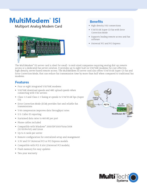
Multiport Analog Modem CardBenefits• High-density , V .92 connections • V .34/33.6K Super G3 fax with Error Correction Mode • Supports leading remote access and fax software • Universal PCI and PCI ExpressThe MultiModem ® ISI server card is ideal for small- to mid-sized companies requiring analog dial-up remote access or a dedicated fax server solution. It provides up to eight built-in V .92/56K modems for cost-effective,high-density , server-based remote access. The MultiModem ISI server card also offers V .34/33.6K Super G3 fax and Error Correction Mode, that can reduce fax transmission time by more than half when compared to traditional fax modems.Features• Four or eight integrated V .92/56K modems• V .92/56K download speeds and 48K upload speeds when connecting with V .92 servers • Class 1.0 and Class 2.1 faxing at speeds to V .34/33.6K bps (Super G3)• Error Correction Mode (ECM) provides fast and reliable fax transmissions • V .44 compression improves data throughput rates • U.S. Caller ID reporting• Sustained data rates to 460.8K per port • Phone cables included• Compatible with Windows ® 2000/XP/2003/Vista/2008 (32-bit/64-bit) and Linux • Up to 4 cards per server• Remote configuration for centralized setup and mangement • 3.3V and 5V Universal PCI or PCI Express models • Compatible with PCI-X slot (Universal PCI models)• Flash memory for easy updates • T wo-year warrantyMultiModem ®ISIWorld Headquarters Tel: (763) 785-3500 (800) EMEA Headquarters Multi-Tech Systems (EMEA)United KingdomTel: +(44) 118-959 7774Multi-Tech Systems (EMEA) FranceTel: +(33) 1 49 19 22 06HighlightsCost-Effective & Scalable. The MultiModem ISI server card provides four or eight dial-up sessions using only one server slot. When demand exceeds one modem card, you can simply add up to three additional cards.V.92 Dial-out Connections. The MultiModem ISI server card supports V .92/56K dial-out and V .34/33.6K dial-inconnections. With V .92 dial-out, you can achieve an upload speed of 48K bps (30% increase over V .90 modems).Enhanced Fax Features. The MultiModem ISI server card supports V .34 fax and Error Correction Mode providingsignificant performance and reliability enhancements over previous fax standards. V .34 sends and receives faxes at speeds up to 33.6K, more than double the speed of the V .17/14.4K fax standard. Error Correction Mode adds reliablility while increasing performance of faxtransmissions. Together these enhancements increase the performance of the MultiModem ISI server card to levels previously only found in more expensive dedicated fax boards and machines.V.44 Compression. V .44 compression standard improves V .42bis data compression anywhere from 20 to 60%, up to as much as 200% for certain types of highly compressible data. This compression technique enables data throughput rates of higher than 300K bps.Simplify Remote Access. The fully-integrated MultiModem ISI server card is easy to set up and manage. You only have to connect the phone lines. There are no external modems and power cords to hassle with; plus it saves back office space since the modems are on the prehensive Service and Support. The Multi-Techcommitment to service means we provide a two-year product warranty and service that includes free telephone technical support, 24-hour web site and ftp support.Ordering InformationProductDescriptionRegion ISI5634UPCI/8 V .92, 8-Modem Card - Universal PCI Global ISI5634UPCI/4 V .92, 4-Modem Card - Universal PCI Global ISI9234PCIE/8 V .92, 8-Modem Card - PCI Express Global ISI9234PCIE/4V .92, 4-Modem Card - PCI ExpressGlobalSpecificationsModemData: V .92, V .90, enhanced V .34, V .32bis, V .22bis Error Correction: V .42, MNP Class 3 & 4Data Compression: V .44, V .42bis, MNP Class 5FaxStandards: V .34, V .17, V .29, V .27ter, V .21, T.30, T.30Annex A, T.30 Annex F , T.31, T.31 Annex B, T.32 Annex C, TR29.2 Class 2 RecommendationRates: 33.6K, 31.2K, 28.8K, 26.4K, 24K, 21.6K, 19.2K, 16.8K, 14.4K, 12K, 9600, 7200, 4800, 2400, 300 bps Error Correction: ECMCompression: MH (T.4), MR (T.4), & MMR (T.6)Conversion: Real time (on-the-fly) compression conversionCommands: Class 1, 2, 1.0, 2.0, 2.1Bus Type3.3V & 5V Universal PCI or PCI Express (x1)Operating System SupportWindows 2000/XP/2003/Vista/2008 (32-bit/64-bit) & LinuxCablingFan out cable with 1 or 2 RJ45 connectors & 4 or 8 RJ11 connectorsPhysical DescriptionUniversal PCI Models:13.87" L × 4.97" W; 8.7 oz (35.2 cm × 12.6 cm; 247 g)PCI Express Models:13.87" L × 4.97" W; 8.5 oz (35.2 cm × 12.6 cm; 241 g)Operating EnvironmentTemperature Range: +23° to +140° F (-5° to +60° C)ApprovalsCE MarkEMC: FCC Part 15 Class B, EN 55022, EN 55024Safety: UL/cUL 60950-1, EN 60950-1, AS/NZS 60950:2000, CCCTelecom: 47CFR Part 68, CS03, TBR21Other countries also includedCopyright © 2008 by Multi-Tech Systems, Inc. All rights reserved.6/08 86000323Made in Mounds View, MN, U.S.A.Features and specifications are subject to change without notice.Trademarks / Registered Trademarks: MultiModem, Multi-Tech, and theMulti-Tech logo: Multi-Tech Systems, Inc. / All other products and technologies are the trademarks or registered trademarks of their respective holders.。
派克汉尼汾中国 H 系列 ISO 阀说明书

目录派克气动销售要约本文档中所述项目可由派克汉尼汾公司、其子公司或授权分销商销售。
此要约及其接受受本文件另一页中题为“销售要约”之条款的约束。
版权所有© 2020,2019派克汉尼汾公司。
保留所有权利P2H 网络节点P2M 网络节点非电路集成连接电路集成连接Turck 网络接口PCH 网络接口• 特性 .................................................................................3-6•电路集成连接 ...............................................................7-29 15407-2 - 尺寸 02, 01 (HB, HA) .....................................8-9 5599-2 - 尺寸 1, 2 (H1, H2) ........................................10-11 尺寸参数 ......................................................................12-21 5599-2 - 尺寸 3 (H3) ...................................................22-29•非电路集成连接 .........................................................30-51 15407-1 - 尺寸 02, 01 (HB, HA) ......................................31 5599-1 - 尺寸 1, 2 (H1, H2) ........................................32-35 订货信息 ......................................................................36-44 5599-1 - 尺寸 3 (H3) ...................................................45-51• 技术参数 / 附件 .........................................................52-66• 尺寸参数 ......................................................................67-77H 系列 ISO 阀网络通讯• 特性 .............................................................................78-89• P2M 网络节点 .............................................................90-97•P2H 网络节点............................................................98-102• PCH 网络接口 .........................................................103-119• H 系列网络接口......................................................120-134• Turck 网络接口 .......................................................135-154•附件 / 电缆..............................................................155-157•技术参数 / 尺寸参数 .............................................158-163H 系列 ISO 阀特性H 系列 ISO 阀H 系列ISO 阀符合国际标准15407和5599,为终端用户提供灵活的设置。
LNK562-564中文资料
PI-4526-040207
版本 E F G H
注释 1) 最终发布的数据手册 1) PI-3924已做修改 1) 增加SO-8封装信息 1) 器件订购部分新增无卤素产品信息
日期 10/05 10/05 2/07 11/08
器件订购信息 LNK 562 D N - TL
LinkSwitch产品系列
LP系列号
封装信息
G 塑封表面贴DIP
P 塑封直插式DIP
D 塑封SO-8封装
无铅封装
N 纯镀锡封装(符合RoHS)
G 满足RoHS及无卤素的法规(仅限P和D封装)
带装&卷轴装及其它包装形式
Blank 标准配置
TL
带装&卷轴装,至少1000个,仅适用于G封装。 D封装有2500个。不适用于P封装。
Life Support Policy POWER INTEGRATIONS PRODUCTS ARE NOT AUTHORIZED FOR USE AS CRITICAL COMPONENTS IN LIFE SUPPORT DEVICES OR SYSTEMS WITHOUT THE EXPRESS WRITTEN APPROVAL OF THE PRESIDENT OF POWER INTEGRATIONS. As used herein:
图10.输出导通
图11.峰值负脉冲漏极点
11
版本H 11/08
LNK562-564
图12.击穿电压与温度的特性曲线
图13.频率与温度的特性曲线
图14.限流点与温度的特性曲线
图15.反射引脚与温度的特性曲线
含氢硅烷偶联剂560资料表

含氢硅烷偶联剂560资料表摘要:一、介绍含氢硅烷偶联剂5601.概述2.应用领域二、含氢硅烷偶联剂560 的性能特点1.化学结构2.物理性质3.反应特性三、含氢硅烷偶联剂560 的使用方法1.常规使用方法2.注意事项四、含氢硅烷偶联剂560 的应用实例1.环氧树脂应用2.玻纤增强应用五、总结正文:一、介绍含氢硅烷偶联剂560含氢硅烷偶联剂560 是一种硅烷偶联剂,具有特殊的化学结构和反应特性,被广泛应用于各种领域。
二、含氢硅烷偶联剂560 的性能特点1.化学结构含氢硅烷偶联剂560 的化学结构中,含有硅、氢、氧等元素,具有独特的分子结构。
2.物理性质含氢硅烷偶联剂560 通常为无色或淡黄色液体,具有较低的粘度,易于混合和施工。
3.反应特性含氢硅烷偶联剂560 具有较高的反应活性,在接触到固化剂时,可以迅速发生化学反应,形成稳定的化学键。
三、含氢硅烷偶联剂560 的使用方法1.常规使用方法含氢硅烷偶联剂560 通常与固化剂一起使用,在环氧树脂、玻纤增强等材料中起到偶联作用。
在使用过程中,需要确保含氢硅烷偶联剂560 与固化剂充分混合,以确保反应的顺利进行。
2.注意事项在使用含氢硅烷偶联剂560 时,需要注意避免与眼睛、皮肤等接触,以免造成刺激。
同时,应储存在阴凉、干燥的地方,防止阳光直射。
四、含氢硅烷偶联剂560 的应用实例1.环氧树脂应用含氢硅烷偶联剂560 可以用于环氧树脂的固化,提高环氧树脂的物理性能和耐候性。
2.玻纤增强应用含氢硅烷偶联剂560 可以用于玻纤增强材料,提高玻纤与基体的粘结力,从而提高材料的整体性能。
五、总结含氢硅烷偶联剂560 作为一种性能优异的偶联剂,在环氧树脂、玻纤增强等领域有着广泛的应用。
含氢硅烷偶联剂560资料表

含氢硅烷偶联剂560资料表一、引言含氢硅烷偶联剂560是一种常用的功能性化学物质,用于改善聚合物与无机材料的粘附性能。
本文将详细探讨含氢硅烷偶联剂560的性质、应用领域以及合成方法等方面的相关内容。
二、含氢硅烷偶联剂560的性质2.1 物理性质•分子量:XXX•外观:XXX•溶解性:XXX•密度:XXX•熔点:XXX•沸点:XXX2.2 化学性质•搭接反应性:XXX•稳定性:XXX•酸碱性:XXX•氧化性:XXX•燃烧性:XXX三、含氢硅烷偶联剂560的应用领域3.1 聚合物改性1.增强聚合物与无机填料的粘附性;2.提高聚合物的力学性能;3.增加聚合物的热稳定性。
3.2 建筑材料1.用于改进水泥基复合材料的性能;2.用作水泥基、树脂基及硅酮等材料和无机表面的粘接促进剂。
3.3 电子材料1.作为导电胶黏剂的增粘剂;2.提高电子封装材料的耐热性和耐湿性。
3.4 涂料和油墨1.提高涂层和油墨的耐候性;2.提高涂层和油墨的附着力。
3.5 橡胶工业1.增强橡胶与无机催化剂的结合力;2.提高橡胶制品的机械性能和耐热性。
四、含氢硅烷偶联剂560的合成方法4.1 原料4.2 合成步骤1.步骤一:XXX2.步骤二:XXX3.步骤三:XXX4.3 反应机理4.4 优化条件和改进方法五、结论含氢硅烷偶联剂560作为一种功能性化学物质,在聚合物改性、建筑材料、电子材料、涂料和油墨、橡胶工业等领域都有重要的应用价值。
本文从物理性质、化学性质、应用领域和合成方法等多个方面对其进行了全面系统的探讨。
随着科学技术的进步和应用领域的扩大,含氢硅烷偶联剂560有望在更多的领域展现出广阔的应用前景。
六、参考文献[1] XXX [2] XXX [3] XXX。
74HC154中文资料_数据手册_参数

QUICK REFERENCE DATA GND = 0 V; Tamb = 25 °C; tr = tf = 6 ns.
HHXXXXHHHHHHHHHH H H H H H H HL XXXXHHHHHHHHHH H H H H H H LHXXXXHHHHHHHHHH H H H H H H L L L L L L LHHHHHHHHH H H H H H H
HL L LHLHHHHHHHH H H H H H H LHL LHHLHHHHHHH H H H H H H HHL LHHHLHHHHHH H H H H H H L LHLHHHHLHHHHH H H H H H H HLHLHHHHHLHHHH H H H H H H LHHLHHHHHHLHHH H H H H H H HHHLHHHHHHHLHH H H H H H H L L LHHHHHHHHHLH H H H H H H HL LHHHHHHHHHHL H H H H H H LHLHHHHHHHHHHH L H H H H H HHLHHHHHHHHHHH H L H H H H L LHHHHHHHHHHHH H H L H H H HLHHHHHHHHHHHH H H H L H H LHHHHHHHHHHHHH H H H H L H HHHHHHHHHHHHHH H H H H H L
notes 1 and 2
TYPICAL
74HC154 74HCT154
11
13
3.5
3.5
Fujitsu 560H 系列 Compact Flash 卡插座连接器说明书

COMPACT FLASH CARD CONNECTORS560H SERIES (CFA COMPATIBLE)s FEATURES•The connectors conform to the Compact Flash Association (CFA) specifications.•The terminal of the plug is a 0.635 mm pitch, one-row, SMT type.•Raised mounting type connectors (standoff), which allow mounting components under a connector, are also available.•The ejector mechanism makes insertion and ejection of a card easier is available.•There are two types of sockets for CFA cards: a straddle mount type and single-sided mounting type.s SPECIFICATIONSs PIN CONNECTOR (PLUG) CONTACT LENGTHsMATERIALSme t I la i r e t a M l a i r e t a m g n i t a l u s n I 0-V 49L U n i s e r S P P :y d ob n i a M 0-V 49L U T B P :e d i u G 0-V 49L U S B A :n o t t u B r o tc ud n o C y o l l a re p p o C gn i t a l P dl o g :t c a t n o C mu i d a l l a p :l a n i m r e T e p y T t c a t n o C .o n n i P h t g n e l t c a t n o C s n i p d n u o r g ,r e w o P 05,83,31,1).n i 691.0(m m 89.4s n i p n o i t c e d d r a C 62,52).n i 731.0(m m 84.3sn i p l a n g i s r e h t O re h t O ).n i 761.0(m m 42.4me t I no i t a c i f i c e p S e g n a r e r u t a r e p m e t g n i t a r e p O C °58+o t °55-t n e r r u c d e t a R C D A 5.0e g a t l o v d e t a R CA V 052e c n a t s i s e r t c a t n o C m 08Ω)A m 01,V m 02C D (x a m e c n a t s i s e r n o i t a l u s n I M 0001Ω,C D V 005,.n i m eg a t l o v d n a t s h t i w c i r t c e l e i D CD V 005RIGHT ANGLE PLUG, SMT TYPE (WITH NO EJECTOR)sDIMENSIONSs PC BOARD MOUNTING PATTERN (MOUNTING SIDE)s ORDERING PART NUMBER FCN-568H050-G/A1For above connector with ejector mechanism see page 3.Unit: mm (in.)Unit: mm (in.)40.16 (1.581)31.115±0.2 (1.225±.008)0.635±0.15(.025±.006)2x Ø2.2(.086)2x 4(0.157)2x2(0.079)35.9 (1.413)50.6 (1.992)16 (.630)19 (.749)25 (.984)26.5 (1.043)1(.039)4.5 (.177)4.5 (.177)1.25(.049)43.03±0.06 (1.225±.002)B30.48 (1.200)No. 13No. 381.27(.050)1.27(.050)1.4±0.05(.055±.002)No. 1No. 13BNo. 25No. 5040.16 (1.581)2x0.89±0.05(.035±.002)0.79±0.06 (.031±.002)1.75 (.069)2.6±0.03 (.102±.0001)2(.079)2.5 (0.098)5.25 (0.207)3.5 (0.138)4.5 (0.177)φ1.5+0 (0.059+0 )-0.1-0.004 3.5±08 (0.138±003)1(0.039)1 (.039)5.1(0.201)2.54 (0.1)1.8(.071)9.5 (0.374)11 (0.433)Section B-BRecommended PCB Pattern2 x 3(.079 x .118)46.13±0.15 (1.816±0.006)40.16±0.05 (1.581±0.002)31.115±0.05 (1.225±0.002)0.635±0.03 (0.025±0.001)2 × φ1.7±0.03(0.67±0.001)2 × φ2.2±0.05 (0.087±0.002)2±0.15(0.079±0.006)7.55±0.05(0.297±0.002)3.5±0.05(0.138±0.002)3±0.1 (.118±0.004)2 × 5±0.15(0.197±0.006)0.4±0.03 (0.016±0.001)No.38No.50No.26No.13No.1No.2547.10 -0 (1.854-0)7.45 (0.293)3.5 (0.138)5.55-0 (0.219-0)3 (.118)7.6-0(0.299-0)20.5-0(0.807-0)1.85-0.1 (0.073-0.004)+0+0The End of the P.C. BoardComponent mounting prohibited areaComponent mounting prohibited areas ORDERING PART NUMBER FOR CONNECTOR/EJECTOR KIT FCN-568H050-G/A1ACRIGHT ANGLE PLUG, SMT TYPE (WITH EJECTOR)sDIMENSIONSUnit: mm (in.)47.6 (1.874)23.8 (0.937)27.3 (1.074)5.5 (0.217)10.65 (0.420) a t c a r d e j e c t e d17.4 (0.685) a t c a r d i n s e r t e d6.75(0.266)29.25 (1.151)10.95 (0.431)28.6 (1.126)7.85 (0.309)0.3 (0.012)5.8 (0.228)1.5 (0.060)Connector/Ejector KitConnector/Ejector mechanism (P/N FCN-560HAC)RIGHT ANGLE PLUG, SMT TYPE (WITH NO EJECTOR, TO BE MOUNTED ON BACK OF PC BOARD)sDIMENSIONSs PC BOARD MOUNTING PATTERN (MOUNTING SIDE)s ORDERING PART NUMBER FCN-568H050-G/A2For above connector with ejector mechanism see page 5.Unit: mm (in.)Unit: mm (in.)40.16 (1.581)31.115±0.15 (1.225±0.006)0.635±0.15(0.025±0.006)2 x φ2.2(0.086)2 X 4(0.157)4.5(0.177)1 (0.039)1(0.039)16 (0.630)19 (0.749)25 (0.984)26.5 (1.043)1.25 (0.049)5.1 (0.201)2.5 (0.098)3.5±08 (0.138±003)5.25 (0.207)3.5 (0.138) 11 (0.433)φ1.50 (0.0590)000035.9 (1.413)2 x 0.89(0.035)50.6 (1.992)43.03±0.06 (1.225±0.002) 1.27(0.050)1.27 x (25-1) = 30.48 (1.200)No. 38No. 262 X 2.0 (0.079)40.16 (1.581)1.400(0.055000)BNo. 50No. 25No. 13 0.79 00(0.031000)No. 11.27 (0.050)4.5 (0.177)1.5(0.059)4.5 (0.177)2.54 (0.1)Section B-BB9.5(0.374) 1.8(0.070)No.13No.1No.25No.50No.38No.262±0.15(0.079±0.006)7.55±0.05 (0.297±0.002)3.5±0.05(0.138±0.002)0.4±0.03 (0.016±0.001)46.13±0.15 (1.816±0.006)0.635 × (50 – 1)= 31.115±0.05 (1.225±0.002)0.635±0.03(0.025±0.001)2 × φ1.7±0.03(0.67±0.001)2 × φ2.2±0.05(0.087±0.002)3±0.1(118±0.004)2 × 5±0.15(0.197±0.006)Recommended PCB pattern47.10 -0 (1.854-0)7.45 (0.293)3.5 (0.138)5.55 (0.219)3 (0.118) 7.6-0(0.299-0)20.5-0(0.807-0)1.85-0.1(0.073-0.004)+0+0The End of the P.C. BoardComponent mounting prohibited areaComponent mounting prohibited area2 x 3(.079 x .118)s ORDERING PART NUMBER FOR CONNECTOR/EJECTOR KIT FCN-568H050-G/A2ADRIGHT ANGLE PLUG, SMT TYPE (WITH EJECTOR, TO BE MOUNTED ON BACK OF PC BOARD)sDIMENSIONSUnit: mm (in.)47.6 (1.874)23.8 (0.937)27.3 (1.874)5.5 (0.217)10.65 (0.420) w h e n c a r d i s e j e c t e d17.4 (0.685)w h e n c a r d i s i n s e r t e d29.25 (1.151)10.95 (0.431)28.6 (1.126)0.3 (0.011)5.8 (0.228)1.5 (0.060)7.85 (0.309)Connector/Ejector KitConnector/Ejector mechanism (P/N FCN-560HAD)RIGHT-ANGLE PLUG, SMT TYPE (WITH NO EJECTOR, 1.64mm RAISED TYPE)sDIMENSIONSs PC BOARD MOUNTING PATTERN (MOUNTING SIDE)s ORDERING PART NUMBER FCN-568H050-G/A3For above connector with ejector mechanism see page 7.Unit: mm (in.)Unit: mm (in.)No.38No.50No.26No.1No.13No.252 × 3(0.079 x 0.118)2±0.15(0.079±0.006)7.55±0.05 (0.297±0.002)3.5±0.05(0.138±0.002)0.4±0.03 (0.016±0.001)46.13±0.15 (1.816±0.006)40.16±0.05 (1.581±0.002)0.635 × (50 – 1)= 31.115±0.05 (1.225±0.002)0.635±0.03 (0.025±0.001)2 × φ1.7±0.03(0.67±0.001)2 × φ2.2±0.05(0.087±0.002)3±0.1 (118±0.004)2 × 5±0.15(0.197±0.006)Recommended PCB patternComponent with 1.1 mm (0.043 in.)or less height can be mounted.47.10 -0 (1.854-0)7.45 (0.293)2.3(0.090)3.5 (0.138)5.55 (0.219)3 (0.118)7.6-0(0.299-0)20.5-0(0.807-0)3.0-0 (0.118-0)1.85-0.1 (0.073-0.004)+0+0The End of the P.C. BoardComponent mounting prohibited area Component mounting prohibited area50.60 (1.992)40.16 (1.581)31.115±0.15 (1.225±0.006)35.9 (1.413)2 x 0.89±0.05(0.035±0.002)2.0 (0.079)1.64 (0.065)2.5 (0.098)43.03±0.06 (1.225±0.002)0.635±0.15 (0.025±0.006)2 x φ2.2(0.086)2x 4(0.157)4.5(0.177)1 (0.039)16 (0.630)19 (0.749)25 (0.984)26.5 (1.043)4.5(0.177)5.25 (0.207)3.5(0.138)4.5 (0.177)11 (0.433)1.75 (0.069)1.27 (0.050)1.27(0.050)0.79 ±0.05(0.031±0.002) 1.4 ±0.05(0.055±0.002)φ1.5+0(0.059+0 )-0.1-0.004No. 1No. 26No. 38No. 13No. 25No. 503.5±08 (0.138±003)1(0.039)6.64 (0.261)BBASection B-B1.25 (0.050)2.54 (0.1)1.5 (0.060)9.5(0.374)1.8(0.070)30.48 (1.2)s ORDERING PART NUMBER FOR CONNECTOR/EJECTOR KIT FCN-568H050-G/A3ACRIGHT-ANGLE PLUG, SMT TYPE (WITH EJECTOR, 1.64mm (0.065 in.) RAISED TYPE)sDIMENSIONSUnit: mm (in.)1.84 (0.072)7.34 (0.289)Connector/Ejector Kit47.6 (1.874)23.8 (0.937)27.3 (1.074)5.5 (0.217)10.65 (0.420)w h e n c a r d i s e j e c t e d17.4 (0.685)w h e n c a r d i s i n s e r t e d6.75(0.266)28.6 (1.126)29.25 (1.151)4.05(0.159)1.5 (0.060)10.95 (0.431)7.85 (0.309)Connector/Ejector mechanism (P/N FCN-560HAC)RIGHT-ANGLE PLUG, SMT TYPE (WITH NO EJECTOR, 1.64mm (0.065) RAISED TYPE, TO BE MOUNTED ON BACK OF PC BOARD)s DIMENSIONSs ORDERING PART NUMBER FCN-568H050-G/A4For above connector with ejector mechanism see page 9.s ORDERING PART NUMBER FCN-568H050-G/A4ADRIGHT-ANGLE PLUG, SMT TYPE (WITH EJECTOR, 1.64mm (0.065 in.) RAISED TYPE, TO BE MOUNTED ON BACK OF PC BOARD)sDIMENSIONSUnit: mm (in.)6.75 (0.265)1.84 (0.072)7.34 (0.289)4.05 (0.159)Ejector mechanism (P/N FCN-560 HAD)Connector/Ejector Kit47.6 (1.874)23.8 (0.937)27.3 (1.074)5.5 (0.217)10.95 (0.431)7.85 (0.309)10.65 (0.420)w h e n c a r d i s e j e c t e d17.4 (0.685)w h e n c a r d i s i n s e r t e d29.95 (1.151)28.6 (1.126)1.5 (0.060)Part No: FCN-560HAC10.95 (0.431)5.5 (0.216)47.6 (1.874)23.8 (0.937)26.75 (1.053)5.5 (0.217)10.65 (0.420)w h e n c a r d i s e j e c t e d17.4 (0.685)w h e n c a r d i s i n s e r t e d28.6 (1.126)4.05(0.159)7.85 (0.309)29.25 (1.151)6.75 (0.266)FCN-560H Series Connector PLUG (Guide)Part No: FCN-560HAD10.95 (0.431)5.5(0.216)47.6 (1.874)23.8 (0.937)27.3 (1.075) 5.5 (0.217)10.65 (0.420)w h e n c a r d i s e j e c t e d17.4 (0.685)w h e n c a r d i s i n s e r t e d4.05(0.159)7.85 (0.309)29.25 (1.151)6.75 (0.266)28.6 (1.126)FCN-560 Series Connector PLUG (GUIDE)560H Series (Compact Flash Connector)11Dimensions are in millimeters (inches) Specifications subject to change© 2001 Fujitsu Components America, Inc. All company and product names are trademarks or registered trademarks of their respective owners. Rev. 09/2001JapanFujitsu Component Limited Gotanda-Chuo Building3-5, Higashigotanda 2-chome, Shinagawa-ku Tokyo 141, Japan Tel: (81-3) 5449-7010Fax: (81-3) 5449-2626Email:************** Web: North and South AmericaFujitsu Components America, Inc.250 E. Caribbean DriveSunnyvale, CA 94089 U.S.A.Tel: (1-408) 745-4900Fax: (1-408) 745-4970Email:*******************.com Web: EuropeFujitsu Components Europe B.V.Diamantlaan 252132 WV Hoofddorp NetherlandsTel: (31-23) 5560910Fax: (31-23) 5560950Email:***************************.com Web: Asia PacificFujitsu Components Asia Ltd.102E Pasir Panjang Road#04-01 Citilink Warehouse Complex Singapore 118529Tel: (65) 375-8560Fax: (65) 273-3021Email:*****************.com Fujitsu Components International Headquarter Offices。
TLV5604中文资料

元器件交易网IMPORTANT NOTICETexas Instruments and its subsidiaries (TI) reserve the right to make changes to their products or to discontinueany product or service without notice, and advise customers to obtain the latest version of relevant informationto verify, before placing orders, that information being relied on is current and complete. All products are soldsubject to the terms and conditions of sale supplied at the time of order acknowledgement, including thosepertaining to warranty, patent infringement, and limitation of liability.TI warrants performance of its semiconductor products to the specifications applicable at the time of sale inaccordance with TI’s standard warranty. Testing and other quality control techniques are utilized to the extentTI deems necessary to support this warranty. Specific testing of all parameters of each device is not necessarilyperformed, except those mandated by government requirements.CERTAIN APPLICATIONS USING SEMICONDUCTOR PRODUCTS MAY INVOLVE POTENTIAL RISKS OFDEATH, PERSONAL INJURY, OR SEVERE PROPERTY OR ENVIRONMENTAL DAMAGE (“CRITICALAPPLICATIONS”). TI SEMICONDUCTOR PRODUCTS ARE NOT DESIGNED, AUTHORIZED, ORWARRANTED TO BE SUITABLE FOR USE IN LIFE-SUPPORT DEVICES OR SYSTEMS OR OTHERCRITICAL APPLICATIONS. INCLUSION OF TI PRODUCTS IN SUCH APPLICATIONS IS UNDERSTOOD TOBE FULLY AT THE CUSTOMER’S RISK.In order to minimize risks associated with the customer’s applications, adequate design and operatingsafeguards must be provided by the customer to minimize inherent or procedural hazards.TI assumes no liability for applications assistance or customer product design. TI does not warrant or representthat any license, either express or implied, is granted under any patent right, copyright, mask work right, or otherintellectual property right of TI covering or relating to any combination, machine, or process in which suchsemiconductor products or services might be or are used. TI’s publication of information regarding any thirdparty’s products or services does not constitute TI’s approval, warranty or endorsement thereof.Copyright © 1999, Texas Instruments Incorporated。
- 1、下载文档前请自行甄别文档内容的完整性,平台不提供额外的编辑、内容补充、找答案等附加服务。
- 2、"仅部分预览"的文档,不可在线预览部分如存在完整性等问题,可反馈申请退款(可完整预览的文档不适用该条件!)。
- 3、如文档侵犯您的权益,请联系客服反馈,我们会尽快为您处理(人工客服工作时间:9:00-18:30)。
ID -- VDS
6.0 V
4.0 V
4.0 3.5 3.0 2.5 2.0 1.5 1.0 0.5 0
ID -- VGS
VDS=10V
0V
V
1.6
8.0
Ta= --25
0 0.5 1.0 1.5 2.0 2.5 3.0 3.5
10.
Drain Current, ID – A
V GS =
1.4 1.2 1.0 0.8 0.6 0.4 0.2 0 0 0.1
Drain Current, ID – A
100 7
7 10 IT01100 1000 7
5
0
0.2
0.4
Ta=7 5°C 25°C --25° C
0.6 0.8
1.0
1.2
1.4 IT01101
Diode Forward Voltage, VSD – V
SW Time -- ID
VDD=15V VGS=10V tr td(off) tf td(on)
Package Dimensions
unit:mm 2168
[CPH5604]
2.9 5 4 3 0.15
0.6
1 0.95
2 0.4
0.6
1.6
2.8
0.05
Specifications
Absolute Maximum Ratings at Ta = 25˚C
Parameter Drain-to-Source Voltage Gate-to-Source Voltage Drain Current (DC) Drain Current (pulse) Allowable Power Dissipation Channel Temperature Storage Temperature Symbol VDSS VGSS ID IDP PD Tch Tstg PW≤10µs, duty cycle≤1% Conditions
Marking : FD
Continued on next page.
Any and all SANYO products described or contained herein do not have specifications that can handle applications that require extremely high levels of reliability, such as life-support systems, aircraft’s control systems, or other applications whose failure can be reasonably expected to result in serious physical and/or material damage. Consult with your SANYO representative nearest you before using any SANYO products described or contained herein in such applications. SANYO assumes no responsibility for equipment failures that result from using products at values that exceed, even momentarily, rated values (such as maximum ratings, operating condition ranges,or other parameters) listed in products specifications of any and all SANYO products described or contained herein.
s
0m
s
op
era
tio
n
0.01 Mounted on a ceramic 2 3 5 7 1.0 0.1
Ta=25°C Single pulse 1 unit
board (600mm2×0.8mm)
2 3 5 7 10 2 3 5 7 100 IT01105
Total Gate Charge, Qg – nC
7 5 3 2
10 7 5 3 2 1.0 7 5 3 2 0.1 7 5 3 2
IF -- VSD
VGS = 0
1.0 7 5 3 2 0.1 0.01
= Ta
C 5° --2
C 75°
C 25°
Forward Current, IF – A
0.01 2 3 5 7 0.1 2 3 5 7 1.0 2 3
Electrical Connection
G1
Switching Time Test Circuit
VDD=15V
G2
S
VIN 10V 0V VIN PW=10µs D.C.≤1%
ID=700mA RL=21.4Ω VOUT
D G
D1
D2
(Top view)
P.G
50Ω
CPH5604
S
2.0 1.8
Gate-to-Source Voltage, VGS – V
8
Drain Current, ID – A
10
7 6 5 4 3 2 1 0 0 0.5 1.0 1.5 2.0 2.5 3.0 3.5 4.0 4.5 5.0
m
10
DC
Operation in this area is limited by RDS(on).
120
140
160
Gate-to-Source Voltage, VGS – V
IT01098
Ambient Temperature, Ta – °C
IT01099
No.6440-2/4
元器件交易网 CPH5604
10
yfs -- ID
VDS=10V
Forward Transfer Admittance, | yfs | – S
600
IT01097
RDS(on) -- VGS
Ta=25°C
RDS(on) -- Ta
Static Drain-to-Source On-State Resistance, RDS(on) – mΩ
Static Drain-to-Source On-State Resistance, RDS(on) – mΩ
元器件交易网 CPH5604
Continued from preceding page.
Parameter Turn-ON Delay Time Rise Time Turn-OFF Delay Time Fall Time Total Gate Charge Gate-to-Source Charge Gate-to-Drain "Miller" Charge Diode Forward Voltage Symbol td(on) tr td(off) tf Qg Qgs Qgd VSD Conditions See specified Test Circuit See specified Test Circuit See specified Test Circuit See specified Test Circuit VDS=10V, VGS=10V, ID=1.4A VDS=10V, VGS=10V, ID=1.4A VDS=10V, VGS=10V, ID=1.4A IS=1.4A, VGS=0 Ratings min typ 7 8 18 8 5 1 1 0.92 1.2 max Unit ns ns ns ns nC nC nC V
元器件交易网
Ordering number:ENN6440
N-Channel Silicon MOSFET
CPH5604
Ultrahigh-Speed Switching Applications
Features
· Low ON resistance. · Ultrahigh-speed switching. · 4V drive. · Composite type with 2 MOSFETs contained in a single package, facilitaing high-density mounting.
0.4
1 : Drain1 2 : Drain2 3 : Gate2 4 : Source 5 : Gate1 SANYO : CPH5
0.2
0.7
0.9
Ratings 30 ±20 1.4 5.6 0.9 150 –55 to +150
0.2
Unit V V A A W ˚C ˚C
Mounted on a ceramic board (600mm2×0.8mm) 1unit
700 600 500 400 300 200 100 0 0 2 4 6 8 10 12 14 16 18 20
500
400
40 I D=
I D=
0m
G A, V
4V S=
V
300
700
m
10 S= A, VG
ID=400mA
700mA
200
100
0 --60
--40
--20
0
20
40
60
80
100
Electrical Characteristics at Ta = 25˚C
Parameter Drain-to-Source Breakdown Voltage Zero-Gate Voltage Drain Current Gate-to-Source Leakage Current Cutoff Voltage Forward Transfer Admittance Static Drain-to-Source On-State Resistance Input Capacitance Output Capacitance Reverse Transfer Capacitance Symbol V(BR)DSS IDSS IGSS VGS(off) | yfs | RDS(on)1 RDS(on)2 Ciss Coss Crss ID=1mA, VGS=0 VDS=30V, VGS=0 VGS=±16V, VDS=0 VDS=10V, ID=1mA VDS=10V, ID=700mA ID=700mA, VGS=10V ID=400mA, VGS=4V VDS=10V, f=1MHz VDS=10V, f=1MHz VDS=10V, f=1MHz 1 1.2 1.7 230 350 90 50 22 300 490 Conditions Ratings min 30 10 ±10 2.4 typ max Unit V µA µA V S mΩ mΩ pF pF pF